1 using dynamic allocation of write voltage to extend ... using dynamic allocation of write voltage...
TRANSCRIPT

1
Using Dynamic Allocation of Write Voltageto Extend Flash Memory Lifetime
Haobo Wang, Student Member, IEEE, Nathan Wong, Student Member, IEEE, Tsung-Yi Chen, Member, IEEE, andRichard D. Wesel, Senior Member, IEEE
Abstract—The read channel of a Flash memory cell degradesafter repetitive program and erase (P/E) operations. This degra-dation is often modeled as a function of the number of P/E cycles.In contrast, this paper models the degradation as a function ofthe cumulative effect of the charge written and erased from thecell. Based on this modeling approach, this paper dynamicallyallocates voltage using lower-voltage write thresholds at thebeginning of the device lifetime and increasing the thresholds asneeded to maintain the mutual information of the read channelin the face of degradation. The paper introduces the techniquein an idealized setting and then removes ideal assumptions aboutchannel knowledge and available voltage resolution to concludewith a practical scheme with performance close to that of theidealized setting.
Index Terms—Flash memory, Channel Estimation, LeastSquares, Dynamic Voltage Allocation, Adaptive Signaling
I. INTRODUCTION
FLASH memory has been widely employed in both con-sumer electronic devices and industrial electronic sys-
tems because of its ability to support high-throughput andlow-latency memory access. However, a fundamental issuewith Flash technology is that its read channel experiencessignificant degradation over time which eventually producesunacceptable reliability. As modern Flash solutions providemore storage capacity in smaller form factors, the resultingincrease of physical cell density and signal constellationdensity amplifies the degradation problem.
The degradation can be addressed in different layers inthe Flash system. At the device layer three-dimensional cellstructures improve durability [1]–[3]. At the system levelchannel codes such as BCH codes [4]–[6] and more recentlyLDPC codes [7]–[10] add redundancy to protect the storedinformation. In [11], the authors write to cells with a lowervoltage but for a longer time to cause less damage at theexpense of increased write time. The resulting scheme pro-vides lifetime extension while still guaranteeing a desired writethroughput.
The degradation over time is often modeled as a functionof the number of program and erase (P/E) cycles, so a direct
This material is based upon work supported partially by Western DigitalInc. Micron Technology Inc. through the UCLA Center on the Developmentof Emerging Storage Systems, and the National Science Foundation underGrant Number 1162501. Any opinions findings, and conclusions or recom-mendations expressed in this material are those of the author(s) and do notnecessarily reflect the views of the National Science Foundation.
H. Wang, N. Wong and R. D. Wesel are with the Department of ElectricalEngineering, University of California, Los Angeles, Los Angeles, CA 90095USA (e-mail: [email protected]; [email protected]; [email protected]).
T.-Y. Chen is with SpiderCloud Wireless Inc., San Jose, CA 95134 USA(e-mail: [email protected]).
Histogram Measurement
Least Squares Parameter Estimation
Histogrgg am MeMM asuruu emee enee t
Leaee st Squqq auu resee Pararr memm ter Estimamm tionoo
Channel Parameter Estimation
DVA Scaling Factor Adjustment
Ev
ery
100
P/E
Cy
cle
s
Fig. 1. Estimation-based DVA framework.
solution is reducing the number of P/E cycles needed. Write-once memory (WOM) codes [12]–[15] provide one approachto reduce the number of P/E cycles required to store infor-mation by permitting multiple writes before an erase cycle isneeded. Another way to reduce the number of P/E cycles isrank modulation [16]–[18], which stores information in thecell using the relative value (or ordering) of cell charge levelsrather than the absolute value. Thus a block of cells can berewritten without erasing by adding charge to properly re-orderthe cells.
Several papers have explored dynamically adjusting to thedegrading read channel [19]–[21]. In [19], read thresholdsare progressively adjusted to minimize hard decoding BERor provide better log-likelihood for soft decoding based onprevious reads. In [20], [21], dynamic threshold assignment(DTA) adjusts the read thresholds to match the shifting andwidening threshold voltage distributions of the read channel,significantly improving bit error rate (BER) performance.
In contrast to the P/E-cycle-based degradation model, thispaper models the degradation as a function of the cumula-tive effect of the charge written and erased from the cell,which we call the accumulated voltage Vacc. The accumulatedvoltage model reveals the opportunity to improve lifetimeby minimizing the Vacc required to store a given amountof information. In particular, this paper explores dynamicallyadjusting the target threshold voltage levels by using lowertarget threshold voltage levels at the beginning of the devicelifetime. This approach is called dynamic voltage allocation(DVA). As the read channel becomes more degraded, thethreshold voltages are gradually increased to what would bethe nominal values in a standard device not employing DVA.As shown in our precursor conference papers [22], [23], DVAmaintains the required mutual information while significantlyextending lifetime.
This is the author's version of an article that has been published in this journal. Changes were made to this version by the publisher prior to publication.The final version of record is available at http://dx.doi.org/10.1109/TCOMM.2016.2607707
Copyright (c) 2016 IEEE. Personal use is permitted. For any other purposes, permission must be obtained from the IEEE by emailing [email protected].
arX
iv:1
609.
0181
6v2
[cs
.IT
] 1
1 O
ct 2
016

2
Fig. 1 illustrates the basic structure of the DVA approach.Periodically (every 100 P/E cycles in the figure) multiple readsusing different read thresholds produce a histogram of thethreshold voltages of the cells on the page or pages con-sidered. A parameter-based least-squares channel estimationdetermines the quality of the read channel from this histogram.Based on the channel estimation, write threshold voltages areset to be as low as possible while still ensuring that the readchannel has sufficient mutual information to be successfullydecoded.
This paper systematically explains and demonstrates theconcept of dynamic voltage allocation, and addresses severalissues to support a practical implementation. This paper ex-tends our previous work [22], [23] in the following ways:
1) Adding programming error and cell-to-cell interferenceto the ground truth channel model;
2) Analyzing DVA’s performance when both estimationand scale-factor adjustment algorithms are simplifiedby using a simple Gaussian model to approximate theunderlying (and more complex) ground truth channel;
3) Designing and analyzing DVA specialized to match aneven-odd structure for writing to cells;
4) Exploring the improvement obtained by DVA over DTA;5) Analyzing DVA’s performance when both write and read
voltage values are restricted to a finite set of availablevoltages;
6) Analyzing DVA’s complexity.This paper begins by introducing DVA in an idealized
setting and then removes ideal assumptions about channelknowledge and threshold resolution to conclude with a practi-cal scheme that has performance similar to that of the idealizedsetting. DVA is first explored under the assumption of perfectknowledge of the channel state as in our precursor conferencepaper [22], except with a more complex read channel thatincludes cell-to-cell interference and programming errors.
Then the performance of DVA is explored when it mustgain its channel information through estimation. All dynamicschemes such as DTA and DVA require some form of infor-mation about the read channel, and different methods can beemployed to acquire the information. For DTA, knowledgeof the voltage distribution is needed. In [20], repetitive readoperations are needed at relatively precise voltages to enablea bisection algorithm to place the read thresholds. In [21],threshold measurements of a certain number of cells arerequired.
As shown in Fig. 1, our approach to acquire read chan-nel information is to measure a limited-resolution histogramand interpret this histogram using certain assumptions aboutthe channel model. In [24], the authors model the Flashread channel as a multi-modal Gaussian distribution withmeans and variances as parameters, and demonstrate that leastsquares algorithms estimate the means and variances well withhistograms having as few as twelve bins. These estimatedparameters are used to set read thresholds according to [25].
This channel estimation is first performed with a perfectchannel model as explored in our precursor conference pa-per [23]. Next, this paper explores the practical scenario inwhich the channel model does not perfectly represent the true
channel. This mismatch is both a reflection of the imperfectcharacterization information available about a specific Flashdevice and the fact that, even with perfect knowledge of thechannel model, simpler models might be preferable becausethey reduce the complexity of estimation.
Next, we explore how constraining the resolution of writeand read thresholds affects performance. We also comparethe performance of DVA to DTA and analyze complexity ofthe DVA framework. Possible solutions to reduce the costof implementing DVA are proposed. Throughout the paper,Multi-level Cell (MLC) Flash (with four levels) is assumedfor all the models and simulations.
The remainder of this paper is organized as follows: Sec. IIpresents the complete channel model. Simplified models areused in some sections. Sec. III introduces DVA using thecomplete channel model but in the idealized setting of perfectchannel state information. Sec. IV formulates the channelparameter estimation problem and presents the least squaresalgorithm and binning strategy used in this paper. Sec. Vexamines the practical scenario in which channel estimationand DVA are based on a model that is not perfect because it issimpler than the actual channel. Sec. VI compares the perfor-mance of DTA and DVA. Sec. VII adds practical constraintson the resolution of the read and write threshold voltages.Sec. VIII analyzes the complexity cost of DVA framework.Sec. IX concludes the paper.
II. MODELING CHANNEL PARAMETERS & DEGRADATION
Because the interfaces are proprietary, we are not able tomeasure data from actual flash devices. Instead, we use themodels introduced in this section to generate the noise thatreflects the behavior of the Flash memory read channel. Thesemodels are called ground truth models, which means that theyare used for all simulations. The term "ground truth model"distinguishes these models from less precise simple Gaussianmodel (which is called the channel model assumption) thatare used by the channel estimation and DVA algorithms. Notethat all algorithms, regardless of the models they incorporatein their calculations, are simulated on the ground truth models.
The ground truth models are not matched to a particularFlash device, but based on the academic publications we citeas we present the models. We believe these models reflectthe major channel degradations and provide a reasonabledegradation trajectory over the lifetime of Flash memory. Weuse these qualitatively correct channel models to show thatDVA can counter the major types of degradation in Flashmemory channels. The models in this section can be replacedwith device-specific models to apply DVA to a particular Flashmemory system. In fact, we will show in Sec. V that DVAdoes not need a precise channel model to provide a significantimprovement in lifetime.
Based on [26]–[37], our precursor conference papers [22]and [23] propose a parameterized channel model characteriz-ing the noise as having three additive components: program-ming noise, wear-out noise, and retention noise. This paperimproves the model of [22] and [23] by adding the effects ofcell-to-cell interference and programming error.
This is the author's version of an article that has been published in this journal. Changes were made to this version by the publisher prior to publication.The final version of record is available at http://dx.doi.org/10.1109/TCOMM.2016.2607707
Copyright (c) 2016 IEEE. Personal use is permitted. For any other purposes, permission must be obtained from the IEEE by emailing [email protected].

3
Voltage
Pro
bab
ilit
y D
ensi
ty
Fig. 2. Flash read channel PDFs illustrating how the probability density ofvoltage thresholds is affected by various noise components.
A. Channel Model with Additive Components
We formulate a Flash memory read channel model with fiveadditive noise components as follows:
y = x+ npe + np + nw + nc2c + nr, (1)
where voltage x is the intended threshold voltage writtento a cell, and y is the measured threshold voltage. Noisenp denotes the programming noise, nw denotes the wear-outnoise, nr denotes the retention noise, nc2c denotes the cell-to-cell interference, and npe denotes the programming error.
Fig. 2 shows an example of voltage distribution probabilitydistribution functions (PDFs) which demonstrates the additiveeffect of each noise component. The arrows in the figurerepresent delta functions.
1) Programming Error npe [38]: Programming errors oc-cur when a bit of the lower page is mis-read in preparation forwriting a bit of the upper page to an MLC cell. Essentially,as the bit of the upper page is written, the error of the firstbit is amplified. The programming error is modeled with aprobability mass function (PMF). For an intended level x,channel parameter Px,y = P (Y = y|X = x) is the conditionalprobability of actually writing y. For MLC Flash, we have
Px,0 + Px,1 + Px,2 + Px,3 = 1, (2)
for each x ∈ {0, 1, 2, 3}. These channel parameters arestrongly related to the number of P/E cycles.
Wordline i
Wordline i+1
(b) Even cell
Vb Vc
VeVd
Va
Wordline i
Wordline i+1
(a) Odd cell
Vb VcVa
Fig. 3. Spacial relationship between the interfering cells (red) and interferedcells (green). Flash memory is written wordline by wordline, i.e., wordlinei+ 1 is written after wordline i. For the interference shown above, within awordline even cells are written before odd cells.
This distortion changes the distribution of stored data. Forexample, if there is no other noise component and the originaldata is uniformly distributed (i.e. each level is equally likely),programming errors move some write thresholds to higherlevels so that the levels are no longer equally likely. Results in[38] indicate that the impact of programming errors becomessignificant only after a large number of P/E cycles.
2) Programming Noise np [22], [23], [26], [27]: Theprogramming noise is modeled as a Gaussian noise for eachlevel, and the noise variance of programmed states is smallerthan that of the erased state because the feedback control loopassociated with programming reduces threshold variation. ThePDF of the programming noise is represented as
fnp(np|x = l) =
{N (0, σ2
e) if l = 0
N (0, σ2p) if l > 0
, (3)
where σe > σp. Index l represents the level of the intendedthreshold voltage level. For MLC Flash, l ∈ {0, 1, 2, 3} wherel = 0 indicates the erased state. Standard deviations σe andσp are the channel parameters for this component, and remainconstant throughout the lifetime of the device.
3) Wear-out Noise nw [22], [23], [28]–[33]: The wear-outnoise is modeled as a positive-side exponential1 noise for eachlevel, and the slope of the distribution is characterized by thechannel parameter λ. The PDF is
fnw(nw) =
{1λe−nwλ if nw ≥ 0,
0 if nw < 0.(4)
Parameter λ increases as the device experiences more P/Ecycles (or larger Vacc).
4) Cell-to-cell Interference nc2c [37], [39]: The cell-to-cell interference experienced by a cell is a weighted sumof the voltage increases in neighboring cells that occur afterthe cell of interest has been written [40]. Fig. 3 shows thespacial relationships between the interfering cells and the cell
1For various device implementations wear-out noise can also be a negative-side exponential or a double-sided exponential (Laplace) distribution. TheDVA and channel estimation techniques we present can be applied in allthese cases.
This is the author's version of an article that has been published in this journal. Changes were made to this version by the publisher prior to publication.The final version of record is available at http://dx.doi.org/10.1109/TCOMM.2016.2607707
Copyright (c) 2016 IEEE. Personal use is permitted. For any other purposes, permission must be obtained from the IEEE by emailing [email protected].

4
µr = −(V − V0) ln(1 +
t
t0
)[Ar
(VaccVmax
)ki+Br
(VaccVmax
)ko](5)
σ2r = 0.1(V − V0) ln
(1 +
t
t0
)[Ar
(VaccVmax
)ki+Br
(VaccVmax
)ko]2(6)
of interest for Flash memories employing the common even-odd structure for writing and for reading. The green circleindicates the cell of interest, and the red circles indicate theinterfering cells. Fig. 3(b) shows that even cells, which arewritten first, suffer interference from the odd cells in thatwordline, which are written after the even cells. As is shownin Fig. 3(a), the odd cells do not suffer any interference fromthe even cells in the same wordline because the odd cells arewritten after the even cells. All the cells in wordline i sufferinterference from the neighboring cells in wordline i+1, whichis written after wordline i. The threshold voltage disturbance(increase) of odd cells Vc2c,odd and even cells Vc2c,even causedby this interference can be modeled as
Vnc2c,odd = γaVa + γbVb + γcVc (7a)Vnc2c,even = Vnc2c,odd + γdVd + γeVe . (7b)
As shown in Fig. 3, Va, Vb, and Vc are voltage increases fromthe cells in the next wordline. Vb is from the cell directlyabove the cell of interest. Va and Vc are voltage increases incells diagonally adjacent on the next wordline that are locatedeither upper left (Va) or upper right (Vc). The voltage increasesVd and Ve are from adjacent cells on the same wordlinethat are to the left (Vd) or right (Ve). When these cells areprogrammed (subsequent to the programming of the cell ofinterest), they interfere with the cell of interest according tothe coupling factors (γ’s) between the interfering cells and thecell of interest. The magnitude of this noise component is thusrelated to two factors: the values of the voltage increases asthe adjacent cells are written to their intended thresholds andthe coupling factors γ.
5) Retention Noise nr [22], [23], [29], [34]–[37]: Theretention noise is modeled as a Gaussian random variable withPDF
fnr (nr) =1
σr√2πe− (nr−µr)2
2σ2r . (8)
Both µr and σ2r (characterized in detail below in Sec. II-B)
are dynamic channel parameters determined by the numberof P/E cycles (or Vacc), retention time and intended thresholdvoltage.
B. Channel Parameter Degradation Model
This subsection presents a model describing how the param-eters describing the additive noise terms degrade as a functionof P/E operations and retention time. From the discussionin Sec. II-A, this degradation occurs for all the channelparameters except those describing the programming noise np.
1) Degradation model due to P/E operations [22], [23]:The degree of damage to a Flash cell’s oxide layer causedby P/E operations is directly related to the volume of chargetraveling through the oxide layer [41]. While the channeldegradation caused by P/E operations is often modeled as afunction of the number of P/E cycles, this model essentiallyassumes that approximately the same volume of charge travelsthrough the oxide layer during each P/E cycle. The novelapproach of DVA is to realize that the intended thresholdvoltages themselves can be varied over time so that lesscharge travels through the oxide layer during early P/E cycleswhen the channel is favorable. Because it is the charge storedin the floating gate that changes the threshold voltage, thedifference between the intended threshold voltage and theerased state voltage is a good indicator of the amount ofcharged transferred. Thus, we define the voltage-based metricVacc/Vmax to characterize P/E cycling where Vacc denotes theaccumulated voltage over P/E cycles
Vacc =N∑
j=1
(V (j)p − Ve), (9)
and Vmax is the maximum voltage difference between pro-grammed and erased states of a Flash cell. In (9), N is thenumber of P/E cycles, V (j)
p is the intended threshold in jthP/E operation, and Ve is the intended threshold voltage ofthe erased state. Only the programming process is consideredin this model, because program and erase are symmetricoperations from the perspective of the amount of chargepassing through the floating gate.
2) Degradation model for the wear-out noise parameter[30], [33]: P/E cycling operations cause the formation of ox-ide traps and interface traps in the cells [28], [29], [31], [32]. In[35] a power law describes how interface trap density dependson P/E cycle count as follows: Aw ·(P/E cycle count)ki , whereki and Aw are constant degradation parameters determinedby the underlying physical properties of the Flash device.Replacing the P/E cycle count with Vacc/Vmax yields ourexpression for interface trap density: Aw · ((Vacc/Vmax)ki .Based on this expression and [30], [33], the wear-out channelparameter λ in (4) has a degradation model that can beformulated as
λ = Cw +Aw ·(VaccVmax
)ki, (10)
where Cw is another constant degradation parameters in addi-tion to ki and Aw .
3) Degradation model for the retention noise parameter[29], [35], [37]: Retention noise models channel degrada-tion in the form a gradual decrease of threshold voltage.
This is the author's version of an article that has been published in this journal. Changes were made to this version by the publisher prior to publication.The final version of record is available at http://dx.doi.org/10.1109/TCOMM.2016.2607707
Copyright (c) 2016 IEEE. Personal use is permitted. For any other purposes, permission must be obtained from the IEEE by emailing [email protected].

5
Both trap recovery and electron detrapping contributes to thisdegradation [34]–[36]. In addition to the interface trap densitymodel, [35] suggests that oxide trap density as well can bemodeled by a power of the P/E cycle count. With the Vacc-based characterization of P/E cycling, total trap density canbe represented as Ar · (Vacc/Vmax)ki + Br · (Vacc/Vmax)ko .From [29], [35], [37], we define the degradation model forthe retention noise channel parameters µr and σ2
r of (4) as(5) and (6) [22], where voltage V is the intended thresholdvoltage, and V0 is the erased state threshold voltage. ki, ko, Arand Br are constant degradation parameters determined by thephysical properties of individual Flash system. Parameter t isthe retention time and t0 is its normalization factor. In thispaper, we study Flash read channel characteristics at a fixedretention target of one year (t = 8760 hours). The techniquespresented in this paper can, of course, be applied for any targetretention time.
4) Cell-to-cell Interference Parameter Model: In [39], theγ parameters in (8) are modeled as random variables withtruncated Gaussian distributions. The authors of [39] mentionthat the means of interfering cells’ γ’s in the next wordlineto be programmed are also random. We simplify the modelby assuming the means of all the γ’s are constant. In ourresearch, the parameter model provided in [39] is utilized,and the cell-to-cell interference strength factor is set to s = 0.2which yields the full set of cell-to-cell interference parametersgiven in the appendix. This setting generates a pair of even-cell and odd-cell read channels with sufficient difference andreasonable typicality.
5) Programming Error Parameter Degradation Model [38]:We employ the programming error parameter degradationmodel proposed in [38]. PX,Y has an exponential relationshipwith P/E cycle counts.
PX,Y = exp(c1x+ c0) (11)
The parameters c1 and c0 are different for each PX,Y , andvariable x indicates the normalized P/E cycle count where themanufacture specified lifetime is used as the normalizationfactor. In this paper, the normalization factor is set to 3000P/E cycles. The resulting PX,Y expressions for our model aregiven in the appendix.
C. Models Used in This PaperThe results presented in this paper are software simulation
results based on two channel models that we have constructedbased on the literature. Model 1 is the channel model usedin [23], which consists of programming noise, wear-out noiseand retention noise. Model 2 is the complete channel modelintroduced in Sec. II-A.
1) Model 1: The channel model in [23] is an exponentiallymodified Gaussian distribution for each level. Cell-to-cellinterference and programming error are not considered in thismodel. As a result, the channel characteristics of even and oddcells are the same. This channel model is still very similar tothe multi-modal Gaussian model.
2) Model 2: The channel model proposed in Sec. II-A dif-ferentiates the even and odd cell read channels, and considersthe effect of programming error and cell-to-cell interference.
III. DYNAMIC VOLTAGE ALLOCATION WITH IDEALCHANNEL INFORMATION
Dynamic Voltage Allocation (DVA) [22] is an algorithm thatuses a single scaling factor α to attenuate the standard thresh-old voltages used to write to the cells. The DVA algorithmcomputes the appropriate scaling factor such that the readchannel achieves at least a certain minimal value of mutualinformation required to support the rate at which informationis stored (the rate indicated by the channel code). The rangebetween the smallest and largest intended voltages is scaled sothat it expands as the channel becomes more degraded until itreaches the range that would be employed in a system withoutDVA. In some Flash devices it may be possible to increase therange beyond the standard range without DVA, but that is nota focus of this paper.
For Flash memory described by Model 1, the mutualinformation is calculated as the difference of marginal andconditional differential entropies as follows [42]:
I(X;Y ) = h(Y )− h(Y |X) . (12)
Random variable Y describes the measured threshold voltage,and X represents the intended threshold voltage. The proba-bility distribution of Y is the channel distribution fY (y), so
h(Y ) = −∫ +∞
−∞fY (y) log (fY (y)) dy . (13)
The relevant conditional differential entropy is calculated as
h(Y |X) = −∫ +∞
−∞
4∑
i=1
fX,Y (xi, y) log(fY |X(y|xi)
)dy ,
(14)Where the joint distribution is fX,Y (x, y) = fY |X(y|x)PX(x),PX(x) is the probability mass function of X , and fY |X(y|x)is the conditional PDF of Y when the cell is written to a singlelevel indicated by x. Let {vi} represent the set of defaultintended threshold voltages, the intended threshold voltageafter scaling is xi = αvi, where α is the scaling factor. As aresult, adjusting the scaling factor will change both h(Y ) andh(Y |X).
Because the cell-to-cell interference of a certain cell is afunction of the threshold voltages of its surrounding cells,the Flash channel described by model 2 is a channel withmemory. From [37], equation (12) is a lower bound on theactual mutual information because it treats interference asindependent noise. Although equation (12) underestimates themutual information, it is still a valid optimization objectivefunction for DVA when cell-to-cell interference is treated asnoise by the controller. If cell-to-cell interference is cancelledby signal processing in the controller, then the portion of cell-to-cell interference that is cancelled should be removed fromthe modeled noise before computing the mutual information.
As discussed in Sec. II, the channel probability distributionfunction is determined by the distributions of the five noisecomponents. In general, the distribution can be calculated byconvolving the five distributions. In [43], a model very similarto the one in Sec. II is presented and the analytical channeldistribution function is calculated. The expression has a rel-atively high complexity. In this paper, numerical convolution
This is the author's version of an article that has been published in this journal. Changes were made to this version by the publisher prior to publication.The final version of record is available at http://dx.doi.org/10.1109/TCOMM.2016.2607707
Copyright (c) 2016 IEEE. Personal use is permitted. For any other purposes, permission must be obtained from the IEEE by emailing [email protected].

6
is used to calculate an approximation of fY |X(y|x). Note thatfor generating noise used in Monte Carlo simulation it is notnecessary to compute this convolution. Rather, the individualnoise terms, each of which is relatively simple in distribution,can be generated and added to the original signal.
Our implementation uses a bisection algorithm to find thescaling factor α. The scaling factor has a range of [0,1], wherea scaling factor of 1 corresponds to the maximum allowedthreshold voltage for each level (the levels that would be usedby a system not implementing DVA). There are two modes forthe DVA algorithm. In the first mode, DVA makes adjustmentsbased on the current channel distribution, and aligns the mutualinformation to a preset threshold that builds in a fixed marginto account for degradation before the scale factor is adjustedagain. In the second mode, DVA makes adjustments based onthe prediction of channel conditions in a future time pointcorresponding to the next DVA scale factor update. In thismode, if the channel model and channel parameter degradationmodels are correct, the mutual information at that futuretime point will be the target value. We use the first modein this paper, because in practice the channel degradationmodels (especially the parameters in the models) may notaccurately reflect the degradation process for device fromdifferent manufactures or for the same device under differentworking conditions (e.g. temperature).
Assuming ideal channel information, which is the exactmodel and parameters of the channel, a simulation can beconducted where the DVA algorithm adjusts the scale-factorevery certain number of P/E cycles. In this paper, DVAfunctions every 100 P/E cycles for simplicity. The number ofP/E cycles between DVA operations depends on how quicklythe channel is varying and the appropriate interval itself mightchange over the lifetime of the device. For example, near theend of life when the channel is degrading rapidly a smallerinterval might be appropriate.
In each iteration of the simulation, the DVA algorithmscales the intended threshold voltages to increase the channelmutual information to a predefined threshold. Because perfectknowledge of the channel state is assumed, the performanceindicates the theoretical limit of the algorithm under these idealconditions. For this ideal simulation we use Model 2, the fullchannel model presented in Sec. II.
DVA is most effective in extending lifetime when the majorchannel degradation is caused by the accumulated effect ofcharge traveling through the oxide layer of the Flash memorycells. Retention loss is the major degradation in this case. Inthis paper, the retention time is set to be a year to representthe worst possible channel for which a device is rated. Ifthe actual retention time exceeds the fixed value, the channelcould still provide enough mutual information depending onthe distance between the actual channel mutual informationand the mutual information limit for the channel code. Dueto page limitations, DVA’s performance when the retentiontime is 0 is not investigated. We believe the lifetime extensionachieved by DVA will be limited in this case.
In this paper, all simulations assume MLC Flash (fourlevels) with each level used equally likely, and the targetmutual information is 1.945 bits per cell for both even and odd
0 1000 2000 3000 4000 5000
P/E Cycle
1.9
1.92
1.94
1.96
1.98
2
)tib(
noita
mrof
nIla
utu
M
Mutual Information with DVA (Even Cell)
Mutual Information with DVA (Odd Cell)
Mutual Information with Fixed Allocation (Even Cell)
Mutual Information with Fixed Allocation (Odd Cell)
Mutual Information Target
Fig. 4. DVA performance with ideal channel information v.s. fixed allocation’sperformance. (Ground truth channel is Model 2. DVA targets even channel.Channel parameters are listed in the appendix.)
channels. Because raw BER is determined by both the channelcondition and the placement of read threshold voltages, thereis no simple way to translate between mutual information andBER. However, simulation results show that a target of 1.945bits achieves a raw BER of 10−2 in Fig. 8 using DTA toallocate read thresholds. We note that the raw BER of 10−2 isshown in [10] to be an operating point for Code 2 in [10] with6 reads using a version of mutual-information-based DTA. Inany case, the mutual information target can be adapted easilyto whatever mutual information is needed to support a specificchannel code (LDPC, BCH, or other). The target for the DVAalgorithm is set to be 1.965 bits to provide an additional 0.02bits of margin above the code-based target to allow for channeldegradation before the next DVA update. The retention timeis set to be one year. The default lifetime measured in P/Ecycles for the programming error model is set to be 3000 P/Ecycles.
The default intended threshold voltages are described by thevector T =
[2.8 5.2 6.4 7.86
][22]. The actual threshold
voltages resulting from DVA updates have the form αT , andFig. 6 shows how the scale factor α varies over time. Whenusing fixed voltage allocation, the scaling factor α is fixedto be 1, so the default intended threshold voltages are usedfor each level through the entire lifetime of the device. Whenusing DVA the scaling factor α starts at a value smaller than1 and increases as the channel degrades until it reaches thevalue of 1 which corresponds to the maximum voltage levelssupported by the device. The full set of channel parameters isgiven in the appendix.
For Flash memories using the even-odd write structurepresented in Sec. II, the even-cell and odd-cell read channelcharacteristics are different as even cells are written beforeodd cells. The even cells experience more severe cell-to-cellinterference and provide less mutual information under thesame intended threshold voltage allocation. One approach tooptimize to this type of Flash memory is to have a single DVAoptimization process controlled by the mutual information of
This is the author's version of an article that has been published in this journal. Changes were made to this version by the publisher prior to publication.The final version of record is available at http://dx.doi.org/10.1109/TCOMM.2016.2607707
Copyright (c) 2016 IEEE. Personal use is permitted. For any other purposes, permission must be obtained from the IEEE by emailing [email protected].

7
0 1000 2000 3000 4000 5000
P/E Cycle
1.9
1.92
1.94
1.96
1.98
2
)tib(
noita
mrof
nIla
utu
M
Mutual Information with DVA (Even Cell)
Mutual Information with DVA (Odd Cell)
Mutual Information with Fixed Allocation (Even Cell)
Mutual Information with Fixed Allocation (Odd Cell)
Mutual Information Target
Fig. 5. DVA performance with ideal channel information and the performanceof the fixed allocation. (The ground truth channel is Model 2. The writingorder of pages is switched every 100 P/E cycles. Joint DVA is use to adjustboth scaling factors for even and odd cells. Channel parameters are listed inthe appendix.)
the even cells, which face the more severe channel conditions.This approach guarantees the worst case performance. Fig. 4shows that with this approach the DVA algorithm can improvethe lifetime of even cells by 65.7% from 2136 P/E cycles to3540 P/E cycles and odd cells by 53.6% from 2517 P/E cyclesto 3867 P/E cycles for the channel defined by the parametersin the appendix. Fig. 6 shows the scale factor α used forall cells (the black curve). Note the rapid reduction in themutual information trajectory shown in Fig. 4 around the endof lifetime. This rapid reduction occurs after the scaling factorhas become one and cannot be further increased as shown inFig. 6.
One problem with the previous approach is that there isa significant performance difference between the even andodd cells. The intended threshold voltages provide too muchmutual information margin for the odd cells. In fact, Fig. 4shows the odd-cell mutual information margin increasing withtime.
This situation is improved by using two separate DVAoptimization processes in the system, one for the even-cellchannel and one for the odd-cell channel. This solution willremove the excessive mutual information margin of the odd-cell channel, but the performance difference measured bylifetime will not be narrowed. One fundamental cause ofthe problem is that even cells experience more accumulateddamage than odd cells.
To address this disparity, we alternate the writing orderbetween even cells and odd cells every 100 P/E cycles. Forexample, even cells are written before odd cells from 0 to99 P/E cycles, and odd cells are written before even cellsfrom 100 P/E cycles to 199 P/E cycles. In this way, thetwo channels can experience similar accumulated damage byswitching which channel receives the more severe cell-to-cellinterference periodically. We apply DVA to this alternating-write-first approach with distinct scaling factors for the even-
0 1000 2000 3000 4000 5000
P/E Cycle
0.4
0.5
0.6
0.7
0.8
0.9
1
rotca
Fgnilac
S
DVA with Write Order Alternation (Even Cell)
DVA with Write Order Alternation (Odd Cell)
DVA Targeting Even Cell Channel (All Cells)
Fixed Voltage Allocation (All Cells)
Fig. 6. Scaling factors generated by DVA with ideal channel information.(Result corresponds to Fig. 4 and 5. Ground truth model is Model 2. Channelparameters are listed in the appendix. The starting value of α is 0.37.)
cell channel and the odd-cell channel, and use a joint DVAalgorithm to adjust the two factors. The mutual informationof the two channels will reach the predefined target togetherafter each iteration. This approach equalizes the accumulatedvoltage Vacc of even-cell and odd-cell channel, and narrows thedifference of the two channels’ characteristics. Fig. 5 showsthat with this approach the DVA algorithm can improve thelifetime of even cells by 68.5% from 2136 P/E cycles to 3600P/E cycles and odd cells by 40.7% from 2517 P/E cycles to3542 P/E cycles for the channel defined by the parameters inthe appendix. Fig. 6 shows the scale factor α used for evenand odd cells as the red and blue curves respectively.
If the overall lifetime is defined as the number of P/E cyclesuntil the mutual information of either channel crosses belowthe 1.945 bits target, joint DVA with the alternating-write-firstapproach extends the lifetime by 65.8% from 2136 P/E cyclesto 3542 P/E cycles. It may seem surprising that the overalllifetime is improved by 65.8% when the lifetime of odd cellsonly improves by 40.7%, but the odd cells were lasting longerthan the even cells to begin with so that the overall lifetimeimprovement is primarily driven by the improvement in theeven cell lifetime.
Recall that the single DVA targeting even-cell channelextends the lifetime by 65.7% from 2136 P/E cycles to 3540P/E cycles, so that the joint DVA did not improve lifetimesignificantly more than the simpler single DVA process forthis channel model. When the strength factor of cell-to-cellinterference s increases, the average distortion of the inter-ference for even-cell and odd-cell channels will rise, and theperformance gain brought by the joint DVA approach will bemore significant. For the remainder of this paper, the joint DVAwith the alternating-write-first approach or its approximationswill be used to implement DVA when the channel model in thesimulation is Model 2, which includes cell-to-cell interference.
IV. CHANNEL PARAMETER ESTIMATION
In order to dynamically allocate intended thresholds in areal system, the channel characteristics must be determined
This is the author's version of an article that has been published in this journal. Changes were made to this version by the publisher prior to publication.The final version of record is available at http://dx.doi.org/10.1109/TCOMM.2016.2607707
Copyright (c) 2016 IEEE. Personal use is permitted. For any other purposes, permission must be obtained from the IEEE by emailing [email protected].
8
dynamically as they evolve. In [24], the authors demonstratethat accurate channel estimation can be achieved with limitedcomputational complexity using multi-modal Gaussian chan-nel model assumption and least squares algorithms. In [23],we further developed this approach with the relatively complexModel 1 channel model, which contains programming noise,wear-out noise and retention noise mentioned in Sec. II-A.
Using both the channel model and the parameter degrada-tion model, the channel characteristics after a specific numberof P/E cycles can be predicted for a specified retention time.However, the exact channel model and parameter degradationmodel need to be known in advance to enable this approach.When considering on-the-fly scenarios, we may also want touse actual measurements from the working device to determinethe channel parameters without making detailed assumptionsabout the parameter degradation model or perhaps even thechannel model itself.
In practical scenarios, empirical histograms of the thresh-old voltage can be measured with multiple read operations.Combined with the knowledge of the read reference voltagesused in the measurements, the empirical distributions provideenough information about the ground truth channel (voltage)distribution. For a given channel model, this measured his-togram can be used to estimate the model parameters usinga least squares algorithm. This approach does not require thechannel parameter degradation model.
In both [23] and [24] , the channel model assumptionsare constructed to be as close to the ground truth model aspossible. In this paper, the idea of using a simple modelassumption, different from the ground truth model, is explored.
A. Channel Parameter Estimation Problem Formation
In this paper, channel parameter estimation is formulatedas an optimization problem as demonstrated in [23]. Oneissue about this approach is that the formulation requires thecalculation of derivatives of certain expressions. If the channelmodel is complex enough, there will be no analytical solutionfor the derivatives, and numerical approximation may need tobe employed. As a result, the accuracy of the estimation couldbe affected. In both [23] and [24], the channel models facilitatethe calculation of analytical derivatives.
B. Binning Strategy and Least Squares Algorithms
In [23], we studied the binning strategy (the assignmentof read threshold voltages that induce the number of binsand the bin placement of the resulting histogram) and theleast square algorithm for histogram-based channel estimationfor a Flash channel under Model 1. In [23], a 9-bin equal-probability binning strategy and Levenberg-Marquardt algo-rithm is demonstrated to have the optimal performance. Thispaper utilizes this result for all simulations.
Because DVA is an iterative process, at every iteration, binplacements are updated based on the channel estimation. Theplacements will only be optimal for the current channel condi-tion even if the estimation is perfect. In order to provide moreaccurate placements for the next iteration, the placements arescaled by the ratio between the newly calculated scaling factor
and the previous scaling factor used before the DVA processin this iteration. This approach provides a linear predictionof bin placements for next iteration’s channel condition, andfacilitates the channel estimation process.
V. DYNAMIC VOLTAGE ALLOCATION WITHMODEL/CHANNEL MISMATCH
When the channel model agrees exactly with the actualchannel, channel estimation can precisely characterize thechannel if the estimated channel parameters are accurate.However, such perfect agreement of the channel model withthe actual channel is hard to achieve in practice because ofthe many factors involved in shaping the Flash read channelcharacteristics. Even if the exact model can be known, thecomplexity of the model may preclude its use in channelestimation and DVA because of the associated complexity.
The lack of perfect agreement limits the precision withwhich the channel can be characterized even with the best-case parameter estimation. However, this problem can becontrolled by selecting a reasonable channel model assumptionthat focuses on the most significant channel characteristics.A good choice can reduce the computational complexity ofchannel estimation and DVA while also capturing the essentialbehavior of the channel.
In [24], the authors investigate a scenario where the channelmodel assumption matches the actual channel and the channelmodel is a relatively simple multi-modal Gaussian distribution.In [23], we demonstrated the estimation performance wherethe channel model matched the actual channel exactly, but themore complex Model 1 of Sec. II-C was used. In both cases,high estimation accuracy is achieved. In this paper, DVA (andimplicitly estimation) performance using the simple multi-modal Gaussian model as the assumption and the complexModels 1 and 2 of Sec. II-C for the actual channel is presented.Thus the channel parameters that need to be estimated formulti-modal Gaussian distribution are the variances and meansof the distribution regardless of the numerous parameters usedto create the actual channel used in the simulation.
A. Model 1
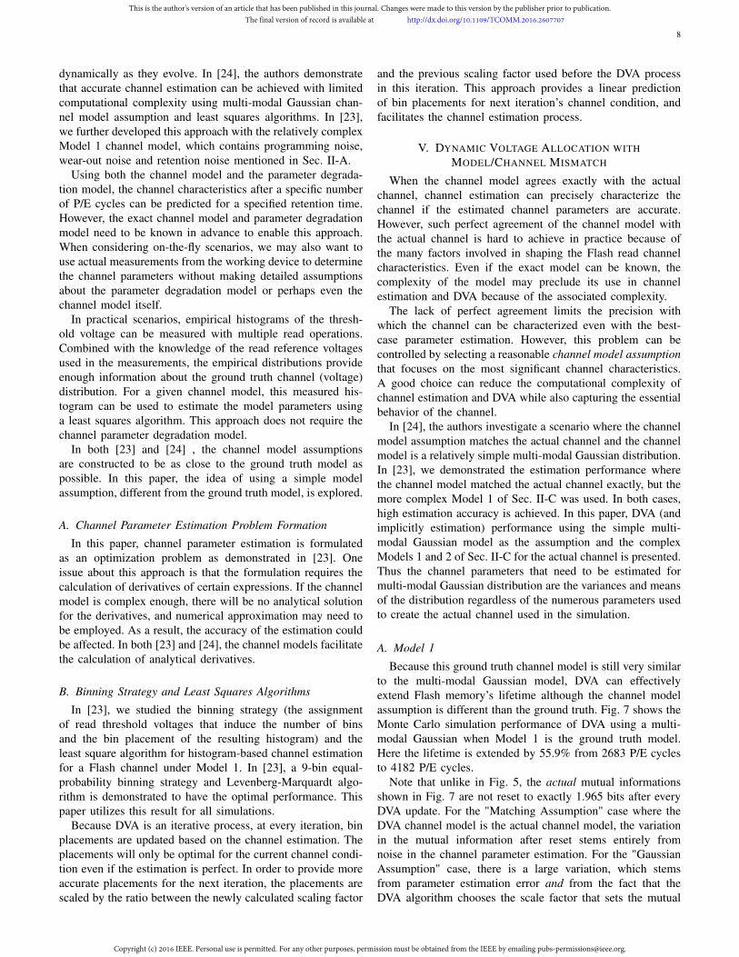
Because this ground truth channel model is still very similarto the multi-modal Gaussian model, DVA can effectivelyextend Flash memory’s lifetime although the channel modelassumption is different than the ground truth. Fig. 7 shows theMonte Carlo simulation performance of DVA using a multi-modal Gaussian when Model 1 is the ground truth model.Here the lifetime is extended by 55.9% from 2683 P/E cyclesto 4182 P/E cycles.
Note that unlike in Fig. 5, the actual mutual informationsshown in Fig. 7 are not reset to exactly 1.965 bits after everyDVA update. For the "Matching Assumption" case where theDVA channel model is the actual channel model, the variationin the mutual information after reset stems entirely fromnoise in the channel parameter estimation. For the "GaussianAssumption" case, there is a large variation, which stemsfrom parameter estimation error and from the fact that theDVA algorithm chooses the scale factor that sets the mutual
This is the author's version of an article that has been published in this journal. Changes were made to this version by the publisher prior to publication.The final version of record is available at http://dx.doi.org/10.1109/TCOMM.2016.2607707
Copyright (c) 2016 IEEE. Personal use is permitted. For any other purposes, permission must be obtained from the IEEE by emailing [email protected].

9
0 1000 2000 3000 4000 5000
P/E Cycle
1.9
1.92
1.94
1.96
1.98
2
)tib(
noita
mrof
nIla
utu
M
Mutual Information with DVA (Matching Assumption)
Mutual Information with DVA (Gaussian Assumption)
Mutual Information with Fixed Allocation
Mutual Information Target
Fig. 7. DVA’s performance with multi-modal Gaussian model. (Ground truthmodel is Model 1. Channel parameters are listed in the appendix.)
information of the multi-modal Gaussian channel to 1.965bits, but the mutual information of the actual channel turnsout to be different. In particular, the mutual information ofthe actual channel is noticeably less than that of the multi-modal Gaussian towards the end of the device lifetime as theGaussian assumption becomes less accurate. Still, the overallDVA approach is successful because the 0.02 bits of additionalmargin was sufficient to overcome the mismatch error.
B. Model 2
For Model 2, the multi-modal Gaussian channel modelassumption can only be considered as a rough approximation,but DVA can still provide a significant performance increaseusing this simple model. Fig. 8 shows the Monte Carlosimulation performance of DVA using the multi-modal channelmodel assumption while generating noise using Model 2. Be-cause the only channel information available is the measuredhistograms from even and odd cells, DVA has to rely onchannel estimation. The channel estimation only provides theestimated means and variances of the multi-modal Gaussianmodel rather than the parameters in the actual channel model.
The estimations of even-cell and odd-cell channels provideapproximated channel characteristics for the odd and evenchannels respectively, when the write order is switched. Basedon this observation, the scaling factors of the two channelscan be updated based on the channel estimation of the otherchannel using DVA. This implementation is an approximationof the joint DVA approach in Sec. III. The simulation resultshows that DVA can extend the overall lifetime by 66.9% from2136 P/E cycles to 3564 P/E cycles for this channel.
Here, it is perhaps surprising that the overall lifetime isimproved more by DVA employing the simple Gaussian modelthan by DVA using the more accurate model and prefectchannel knowledge in Fig. 5. The Gaussian model under-estimates the severity of the channel which causes it to use asmaller value of α that turns out to still provide sufficientmutual information. This extends lifetime a bit more by
0 1000 2000 3000 4000 5000
P/E Cycle
1.9
1.92
1.94
1.96
1.98
2
)tib(
noita
mrof
nIla
utu
M
Mutual Information with DVA (Even Cell)
Mutual Information with DVA (Odd Cell)
Mutual Information with Fixed Allocation (Even Cell)
Mutual Information with Fixed Allocation (Odd Cell)
Mutual Information Target
Fig. 8. DVA performance with multi-modal Gaussian model. The Groundtruth model is Model 2. Channel parameters are listed in the appendix. Thelifetime of even cells is extended by 70.5% from 2136 P/E cycles to 3642P/E cycles. The lifetime of odd cells is extended by 41.6% from 2517 P/Ecycles to 3564 P/E cycles. The overall lifetime is extended by 66.9% from2136 P/E cycles to 3564 P/E cycles.
reducing the amount of charge written. Of course we couldlower the amount of margin used in the simulation of Fig. 5and also gain this benefit.
VI. COMPARISON OF DYNAMIC VOLTAGE ALLOCATIONAND DYNAMIC THRESHOLD ASSIGNMENT
Both dynamic voltage allocation and dynamic thresholdassignment (DTA) [20], [21] track the degradation of Flashmemory channel during its lifetime. DTA allocates appropriateread threshold voltages under different channel conditions toreduce the asymmetric errors caused by distribution shiftingand widening. DVA allocates appropriate write threshold volt-ages under different channel conditions to adjust the mutualinformation to a sufficient (but not extravagant) level. DVAdepends on the preset target mutual information which relatesto the capability of error correction codes employed. Consid-ering Flash memory as a M-ary baseband Pulse AmplitudeModulation (MPAM) communication system (4PAM in thispaper), DTA provides hard decision thresholds closer to theoptimal ones than fixed read thresholds, and DVA adjusts theaverage symbol power of the constellation to match channelconditions.
Assume the simplest fixed-read-voltage allocation schemeswhere hard decision boundaries are put in the midpointsbetween adjacent write threshold voltages, and DTA imple-mentation from [21], simulations are conducted to compare theperformance of DTA alone and DTA combined with DVA. Fig.9 compares the raw BER (without error correction code) ofreading with a fixed voltage allocation, DTA and DVA. Thedash line in the figure represents the raw BER requirementfor the LDPC code in [10] to function properly with softinformation from 6 reads (Fig. 11 in [10]). To accommodatethe rapid channel degradation at the beginning of the lifetimeand meet the 10−2 raw BER target, the scaling factor for botheven and odd cells are lower bounded by 0.45.
This is the author's version of an article that has been published in this journal. Changes were made to this version by the publisher prior to publication.The final version of record is available at http://dx.doi.org/10.1109/TCOMM.2016.2607707
Copyright (c) 2016 IEEE. Personal use is permitted. For any other purposes, permission must be obtained from the IEEE by emailing [email protected].

10
0 1000 2000 3000 4000 5000
P/E Cycle
10-3
10-2
10-1
BER
Fixed - Fixed (Even Cell)
Fixed - Fixed (Odd Cell)
Fixed - DTA (Even Cell)
Fixed - DTA (Odd Cell)
DVA - DTA (Even Cell)
DVA - DTA (Odd Cell)
Fig. 9. DTA and DVA’s performance. (Even and odd cells switch positionswhen using DVA. The legend follows the format write voltage allocationalgorithm - read voltage allocation algorithm. Comparing the result fromDVA - DTA with Fixed - DTA, The lifetime of even cells is extended by66.5% from 2282 P/E cycles to 3800 P/E cycles. The lifetime of odd cellsis extended by 41.4% from 2654 P/E cycles to 3754 P/E cycles. The overalllifetime is extended by 64.5% from 2282 P/E cycles to 3754 P/E cycles.)
Because the retention time is fixed to be one year in oursimulations and there is no operation on the cells duringthis period, the stored voltage values in the cells sufferrelatively significant shifts. As a result, fixed read voltageallocation provides very bad BER performance. With DTA,the read thresholds are able to track the channel degradation,thus produces BER performance consistent with the channelcapacity using fixed write voltage allocation. DVA allocateswrite thresholds to maintain a reasonable channel capacity, soa non-zero low level raw BER appears from the beginning ofthe device’s lifetime, and it is expected to be easily correctedby error correction codes. However, this is in contrast to DTAwithout DVA, where almost no errors occur in the first 1000P/E cycles.
To achieve good raw BER performance, DVA requiresthat DTA-like algorithms are used in conjunction to providedecision boundaries that adapt to the changing write lev-els. Even without DVA, DTA-like algorithms are a practicalnecessity in order to track the movements of the channeldistribution caused by channel degradations such as retentionloss. Fig. 9 shows that DVA and DTA combined provide asignificant performance improvement over DTA alone. Theresults indicate that DVA with DTA can extend the overalllifetime by 64.5% from 2282 P/E cycles to 3754 P/E cyclesfor this ground truth channel model compared with a fixedwrite-voltage allocation with DTA.
VII. DYNAMIC VOLTAGE ALLOCATION WHEN VOLTAGEPLACEMENTS ARE QUANTIZED
In this section, we explore the performance of the DVAframework when voltage placements are limited to certainlocations. In practice, hardware implementations introduce theconstraint that both the read reference voltages and the in-tended write threshold voltage levels can only be set to certain
0 1000 2000 3000 4000 5000
P/E Cycle
1.9
1.92
1.94
1.96
1.98
2
)tib(
noita
mrof
nIla
utu
M
Mutual Information with DVA (Even Cell)
Mutual Information with DVA (Odd Cell)
Mutual Information with Fixed Allocation (Even Cell)
Mutual Information with Fixed Allocation (Odd Cell)
Mutual Information Target
Fig. 10. DVA performance with quantized placements. (Quantization provides64 possible locations. Ground truth model is Model 2. Channel parametersare listed in the appendix.)
0 1000 2000 3000 4000 5000
P/E Cycle
1.9
1.92
1.94
1.96
1.98
2
)tib(
noita
mrof
nIla
utu
M
Mutual Information with DVA (Even Cell)
Mutual Information with DVA (Odd Cell)
Mutual Information with Fixed Allocation (Even Cell)
Mutual Information with Fixed Allocation (Odd Cell)
Mutual Information Target
Fig. 11. DVA’s performance with quantized placements. (Quantizationprovides 128 possible locations. Ground truth model is Model 2. Channelparameters are listed in the appendix. The lifetime of even cells is extendedby 72.1% from 2136 P/E cycles to 3676 P/E cycles. The lifetime of odd cellsis extended by 34.8% from 2517 P/E cycles to 3393 P/E cycles. The overalllifetime is extended by 58.8% from 2136 P/E cycles to 3393 P/E cycles.)
values. This will add an additional constraint to both theintended threshold voltages and the read reference voltages,which affects DVA performance.
Monte Carlo simulation of DVA under several commonlyused voltage quantization scenarios (64, 128 and 256-locationquantization for the entire available voltage range) are con-ducted. We assume adjacent potential placement locationsare separated by a constant distance, which corresponds toequal interval sampling over a certain voltage range. Thequantization range is set to be from -1 Volt to 8 Volts. Figs.10 and 11 show the mutual information v.s. P/E cycle curvewhen limiting the number of possible locations 64 and 128.Quantization with 256 possible locations results a performancevery similar to Fig. 8. Quantization with 128 possible locationsstrikes a nice balance between DVA performance and the num-
This is the author's version of an article that has been published in this journal. Changes were made to this version by the publisher prior to publication.The final version of record is available at http://dx.doi.org/10.1109/TCOMM.2016.2607707
Copyright (c) 2016 IEEE. Personal use is permitted. For any other purposes, permission must be obtained from the IEEE by emailing [email protected].

11
TABLE ICOMPUTATIONAL COMPLEXITY OF READ THRESHOLD VOLTAGE
ALLOCATION
No. of ops. per iter. ADD DIV LUT No. of iterations
Boundary 1 (leftmost) 9 4 4 log2Vr,max−Vr,min
ε
Boundary i, 2 ≤ i ≤ N − 1 9 4 4 log2Vr,max−Vr,i−1
ε
Note: "ops." is the abbreviation for "operations". "iter." is the abbreviation for "iteration".The number of bins in the histogram is N . The ith boundary is Vr,i. The maximumand minimum possible read threshold voltage is Vr,max ans Vr,min respectively. Thetolerance (error) of the bisection algorithm is ε. ADD, DIV, LUT represent addition,division and table lookup operation respectively.
ber of placement locations. When using 128-level quantization,the overall lifetime is extended by 58.8% from 2136 P/E cyclesto 3393 P/E cycles.
Notice that the DVA framework often produces mutualinformation values that are too high (hence leading to a fasterincrease in Vacc and faster degradation) when the numberof possible placement locations is constrained to 64. Wealso observed that under this condition, the quantized readthreshold voltage placements also suffered. Even though onlynine reads are performed, with only 64 possible values, twoor more would be in the same place. As a result, the effectiveresolution of the measured histogram is reduced, and thechannel parameter estimation algorithm becomes less accurateand degrades DVA performance.
VIII. COMPLEXITY ANALYSIS
The DVA framework consists of two processes: channelparameter estimation and scaling factor adjustment. This sec-tion considers complexity for the case discussed in Sec. Vwhere we use a multi-modal Gaussian distribution as thechannel model for both channel parameter estimation and scal-ing factor adjustment. For the channel parameter estimationprocess, there are two steps: read threshold voltage assignmentand iterative Levenberg-Marquardt parameter estimation. Thecomputational complexity of DVA can be analyzed accordingto these three primary components: read threshold voltageassignment, iterative Levenberg-Marquardt parameter estima-tion, and scaling factor adjustment.
Read threshold voltage assignment is used to provideboundaries for the bins in the histogram satisfying the equal-probability binning strategy discussed in Sec. IV-B. In theDVA framework, this assignment is calculated using a Gaus-sian channel model and the estimated channel parameters(means and variances) from the parameter estimation process100 P/E cycles ago. Integration of a Gaussian probability dis-tribution function is needed, but the operation is in essence theevaluation of the Q-function (tail probability of the standardnormal distribution), and can be implemented with a look-up table. The exact position of each read is calculated usingbisection method. Table I summarizes the number of additions(ADD), divisions (DIV) and table lookups (LUT) in eachiteration, and the number of iterations required to calculateeach read threshold voltage.
The computational complexity of using the Levenberg-Marquardt algorithm based on the Gaussian channel model
TABLE IICOMPUTATIONAL COMPLEXITY OF LEVENBERG-MARQUARDT
ALGORITHM
ADD MUL DIV LUT
No. of ops. per iter. 93N + dN3
3e 89N + dN3
3e 4N + dN3
3e 8N
Note: "ops." is the abbreviation for "operations". "iter." is the abbreviation for "iteration".The number of bins in the histogram isN . The tolerance (error) of the bisection algorithmis ε. ADD, MUL, DIV, LUT represent addition, multiplication, division and table lookupoperation respectively.
TABLE IIICOMPUTATIONAL COMPLEXITY OF SCALING FACTOR ADJUSTMENT
ExADD ExMUL MI No. of iterations
5 4 1 log2αmax−αmin
ε
(a) Number of operations per iteration
ADD MUL DIV LUT
44n− 1 88n+ 1 42n 8n
(b) Number of operations per MI
Note: The maximum and minimum possible scaling factor are αmax and αminrespectively. The tolerance (error) of the bisection algorithm is ε. ExADD, ExMUL,MI represent extra addition, extra division in additional to the calculation of mutual in-formation, and mutual information calculation respectively. The number of sample pointsused in MI calculation is n. ADD, MUL, DIV, LUT represent addition, multiplication,division and table lookup operation respectively.
assumption to estimate the Flash read channel is carefullyanalyzed in [24]. The results are summarized here in TableII. Note that the dN3
3 e term in the table comes from theinversion operation of an N × N matrix using the Gauss-Jordan method, where N is the number of bins in the measuredhistogram. Because the Levenberg-Marquardt algorithm hasmultiple stopping criteria, the exact number of iterationsneeded is not a fixed value for different channel conditions.In our simulations, we observe that the maximum number ofiterations is less than 100.
The scaling factor adjustment process uses a bisectionalgorithm to search for the smallest scaling factor that achievesthe mutual information target given the estimated meansand variances. Table III(a) summarizes the number of extraadditions (ExADD), multiplications (ExMUL) other than theones in the mutual information calculation, the number ofmutual information calculations (MI) in each iteration, and thenumber of iterations required to calculate the scaling factor.The most computation-heavy operation in this process is thecalculation of the mutual information (MI) of a multi-modalGaussian distribution, which involves integration operations.Assuming the Gauss-Hermite quadrature [44] method is usedto approximate the integration, the mutual information calcu-lation needs to be represented in the form of
∞∫
−∞
e−x2
f(x)dx , (15)
where f(x) is a function. Then the following approximation
This is the author's version of an article that has been published in this journal. Changes were made to this version by the publisher prior to publication.The final version of record is available at http://dx.doi.org/10.1109/TCOMM.2016.2607707
Copyright (c) 2016 IEEE. Personal use is permitted. For any other purposes, permission must be obtained from the IEEE by emailing [email protected].

12
can be used:
∞∫
−∞
e−x2
f(x)dx ≈n∑
i=1
wif(xi) , (16)
where xi’s are the roots of the Hermite polynomial Hn(x),wi’s are the weights calculated by
2n−1n!√π
n2[Hn−1(xi)]2, (17)
and n is the number of sample points. The accuracy of theapproximation increases with n. Following (12-14), the newmutual information representation is
I(X,Y ) = − 1
4√π
4∑
i=1
∞∫
−∞
e−z2i log(g(zi))dzi , (18)
where
g(zi) =1
4+
4∑
j=1j 6=i
σi4σj
ez2i−
(√
2σizi+xi−xj)2
2σ2j . (19)
Assuming all the weights can be pre-calculated, and log(·), e(·)can be calculated with lookup tables, the number of operationsneeded for each MI calculation is shown is Table III(b).
IX. CONCLUSION
This paper introduces a framework to extend Flash memorylifetime by dynamic allocation of intended threshold voltagelevels based on the current mutual information of the Flashread channel. Analysis and simulation results demonstratethat this framework can provide significant lifetime extensionin practical settings. Simple channel models can be used toestimate a complex Flash channel, and optimize the voltageplacements. Good performance can be achieved even whenthe placement of voltages is constrained to 128 possiblevalues. The frame can be modified to reduce computationalcomplexity while providing comparable performance to a fullyimplemented system.
The results in this paper can be improved by extending theground truth channel models to include additional mechanismsfor channel degradation in Flash memory and by using datameasured from actual Flash devices. Another direction tofurther develop the DVA framework is to explore using rawBER as the optimization target for the DVA framework.
APPENDIXCHANNEL PARAMETERS USED IN THIS PAPER
Programming Noise [22]σe 0.35 σp 0.05
Wear-out Noise [22]Aw 1.8× 10⁻⁴ Cw 1.26× 10⁻³
ki 0.62 —— ——Retention Noise [22]
Ar 7.0× 10⁻⁴ Br 4.76× 10⁻³
ki 0.62 ko 0.3t0 1(hour) t 8760
Cell-to-cell Interference [39]E{γx} 0.1s E{γy} 0.08sE{γxy} 0.006s s 0.2wk 0.2E{γk} σk 0.3E{γk}
Programming Error [38]P0,2 exp(0.87x-11.89) P0,3 exp(1.41x-19.82)P1,2 exp(1.63x-19.22) P1,3 exp(0.73x-11.67)P2,3 exp(1.50x-17.69) —— ——
Default intended threshold voltages [22]: [2.8, 5.2, 6.4, 7.86].Vmax = 16. [22]
REFERENCES
[1] J. Choi and K. S. Seol, “3d approaches for non-volatile memory,” inProc. 2011 Symp. VLSI Technology (VLSIT), 2011, pp. 178–179.
[2] K. Park, D. Byeon, and D. Kim, “A world’s first product ofthree-dimensional vertical NAND Flash memory and beyond,”presented at 2014 14th Annu. Non-Volatile Memory TechnologySymp. (NVMTS), Jeju Island, ROK, Oct. 27-29, 2014.
[3] J. Im et al., “A 128gb 3b/cell V-NAND flash memory with 1gb/s I/Orate,” in 2015 IEEE Int. Solid-State Circuits Conf. (ISSCC) Tech. Dig.,2015, pp. 110–112.
[4] B. Chen, X. Zhang, and Z. Wang, “Error correction for multi-levelNAND flash memory using Reed-Solomon codes,” in Proc. 2008 IEEEWorkshop on Signal Process. Syst. (SiPS), 2008, pp. 94–99.
[5] S. Cho, D. Kim, J. Choi, and J. Ha, “Block-wise concatenated BCHcodes for NAND Flash memories,” IEEE Trans. Commun., vol. 62,no. 4, pp. 1164–1177, Apr. 2014.
[6] D. Kim and J. Ha, “Quasi-primitive block-wise concatenated BCHcodes for NAND flash memories,” in 2014 IEEE Inform. TheoryWorkshop (ITW), 2014, pp. 611–615.
[7] Y. Maeda and H. Kaneko, “Error control coding for multilevel cellFlash memories using nonbinary low-density parity-check codes,” inProc. 2009 24th IEEE Int. Symp. on Defect and Fault Tolerance inVLSI Systems (DFT), 2009, pp. 367–375.
[8] K. Zhao et al., “LDPC-in-SSD: Making advanced error correctioncodes work effectively in solid state drives,” in Proc. 11th USENIXConf. on File and Storage Technologies, 2013, pp. 243–256.
[9] F. Zhang, H. D. Pfister, and A. Jiang, “LDPC codes for rankmodulation in flash memories,” in Proc. 2010 IEEE Int. Symp. onInform. Theory (ISIT), 2010, pp. 859–863.
[10] J. Wang et al., “Enhanced precision through multiple reads for LDPCdecoding in Flash memories,” IEEE J. Sel. Areas Commun., vol. 32,no. 5, pp. 880–891, May 2014.
[11] J. Jeong, S. S. Hahn, S. Lee, and J. Kim, “Improving NANDendurance by dynamic program and erase scaling,” presented at the5th USENIX Conf. on Hot Topics in Storage and File Syst., San Jose,CA, Jun 27-28, 2013.
[12] R. L. Rivest and A. Shamir, “How to reuse a "write-once" memory,”Infor. and Control, vol. 55, no. 1-3, pp. 1–19, Oct. 1982.
[13] A. Jiang, “On the generalization of error-correcting WOM codes,” inProc. 2007 IEEE Int. Symp. on Inform. Theory (ISIT), 2007, pp.1391–1395.
[14] E. Yaakobi, S. Kayser, P. H. Siegel, A. Vardy, and J. K. Wolf, “Codesfor write-once memories,” IEEE Trans. Inf. Theory, vol. 58, no. 9, pp.5985–5999, Sep. 2012.
This is the author's version of an article that has been published in this journal. Changes were made to this version by the publisher prior to publication.The final version of record is available at http://dx.doi.org/10.1109/TCOMM.2016.2607707
Copyright (c) 2016 IEEE. Personal use is permitted. For any other purposes, permission must be obtained from the IEEE by emailing [email protected].

13
[15] R. Gabrys and L. Dolecek, “Constructions of nonbinary WOM codesfor multilevel Flash memories,” IEEE Trans. Inf. Theory, vol. 61,no. 4, pp. 1905–1919, Apr. 2015.
[16] A. Jiang, M. Schwartz, and J. Bruck, “Error-correcting codes for rankmodulation,” in Proc. 2008 IEEE Int. Symp. Inform. Theory (ISIT),2008, pp. 1736–1740.
[17] A. Mazumdar, A. Barg, and G. Zemor, “Constructions of rankmodulation codes,” IEEE Trans. Inf. Theory, vol. 59, no. 2, pp.1018–1029, Feb. 2013.
[18] M. Qin, A. Jiang, and P. H. Siegel, “Parallel programming of rankmodulation,” in Proc. 2013 IEEE Int. Symp. Inform. Theory (ISIT),2013, pp. 719–723.
[19] B. Peleato, R. Agarwal, J. M. Cioffi, M. Qin, and P. H. Siegel,“Adaptive read thresholds for nand flash,” IEEE Trans. Commun.,vol. 63, no. 9, pp. 3069–3081, Sep. 2015.
[20] H. Zhou, A. Jiang, and J. Bruck, “Error-correcting schemes withdynamic thresholds in nonvolatile memories,” in Proc. 2011 IEEE Int.Symp. Inform. Theory (ISIT), 2011, pp. 2143–2147.
[21] F. Sala, R. Gabrys, and L. Dolecek, “Dynamic threshold schemes formulti-level non-volatile memories,” IEEE Trans. Commun., vol. 61,no. 7, pp. 2624–2634, Jul. 2013.
[22] T. Chen, A. R. Williamson, and R. D. Wesel, “Increasing flashmemory lifetime by dynamic voltage allocation for constant mutualinformation,” in Proc. 2014 Inform. Theory and Applicat. Workshop(ITA), Feb. 2014, pp. 1–5.
[23] H. Wang, T. Chen, and R. D. Wesel, “Histogram-based Flash channelestimation,” in Proc. 2015 IEEE Int. Conf. Commun. (ICC), 2015, pp.283–288.
[24] D. Lee and W. Sung, “Estimation of NAND Flash Memory ThresholdVoltage Distribution for Optimum Soft-Decision Error Correction,”IEEE Trans. Signal Process., vol. 61, no. 2, pp. 440–449, Jan. 2013.
[25] J. Wang, T. Courtade, H. Shankar, and R. Wesel, “Soft information forLDPC decoding in Flash: mutual-information optimized quantization,”presented at 2011 IEEE Global Telecommun. Conf. (GLOBECOM),Houston, TX, Dec. 5-9, 2011.
[26] K. Takeuchi, T. Tanaka, and H. Nakamura, “A double-level-Vth selectgate array architecture for multilevel NAND flash memories,” IEEE J.Solid-State Circuits, vol. 31, no. 4, pp. 602–609, Apr. 1996.
[27] C. Compagnoni et al., “First evidence for injection statistics accuracylimitations in NAND Flash constant-current Fowler-Nordheimprogramming,” in Proc. 2007 IEEE Int. Electron Devices Meeting(IEDM), 2007, pp. 165–168.
[28] P. Olivo, B. Ricco, and E. Sangiorgi, “High-field-inducedvoltage-dependent oxide charge,” Appl. Physics Lett., vol. 48, no. 17,pp. 1135–1137, Apr. 1986.
[29] N. Mielke et al., “Flash EEPROM threshold instabilities due to chargetrapping during program/erase cycling,” IEEE Trans. Device Mater.Rel., vol. 4, no. 3, pp. 335–344, Sep. 2004.
[30] K. Fukuda, Y. Shimizu, K. Amemiya, M. Kamoshida, and C. Hu,“Random telegraph noise in flash memories - model and technologyscaling,” in Proc. 2007 IEEE Int. Electron Devices Meeting (IEDM),2007, pp. 169–172.
[31] P. Cappelletti, R. Bez, D. Cantarelli, and L. Fratin, “Failuremechanisms of flash cell in program/erase cycling,” in Proc. 1994IEEE Int. Electron Devices Meeting (IEDM), 1994, pp. 291–294.
[32] S. Yamada et al., “Degradation mechanism of flash EEPROMprogramming after program/erase cycles,” in Proc. 1993 IEEE Int.Electron Devices Meeting (IEDM), 1993, pp. 23–26.
[33] C. Compagnoni, M. Ghidotti, A. Lacaita, A. Spinelli, and A. Visconti,“Random telegraph noise effect on the programmed threshold-voltagedistribution of Flash memories,” IEEE Electron Device Lett., vol. 30,no. 9, pp. 984–986, Sep. 2009.
[34] N. Mielke, H. Belgal, A. Fazio, Q. Meng, and N. Righos, “Recoveryeffects in the distributed cycling of Flash memories,” in Proc. 200642nd Annu. IEEE Int. Reliability Physics Symp., 2006, pp. 29–35.
[35] H. Yang et al., “Reliability issues and models of sub-90nm NANDFlash memory cells,” in Proc. 2006 8th Int. Conf. Solid-State andIntegrated Circuit Technology, 2006, pp. 760–762.
[36] J. Lee, J. Choi, D. Park, and K. Kim, “Data retention characteristics ofsub-100 nm NAND flash memory cells,” IEEE Electron Device Lett.,vol. 24, no. 12, pp. 748–750, Dec. 2003.
[37] G. Dong, Y. Pan, N. Xie, C. Varanasi, and T. Zhang, “Estimatinginformation-theoretical NAND Flash memory storage capacity and itsimplication to memory system design space exploration,” IEEE Trans.VLSI Syst., vol. 20, no. 9, pp. 1705–1714, Sep. 2012.
[38] T. Parnell, N. Papandreou, T. Mittelholzer, and H. Pozidis, “Modellingof the threshold voltage distributions of sub-20nm NAND flashmemory,” in Proc. 2014 IEEE Global Commun. Conf. (GLOBECOM),2014, pp. 2351–2356.
[39] G. Dong, S. Li, and T. Zhang, “Using data postcompensation andpredistortion to tolerate cell-to-cell interference in MLC NAND Flashmemory,” IEEE Trans. Circuits Syst. I, vol. 57, no. 10, pp. 2718–2728,Oct. 2010.
[40] J. Lee, S. Hur, and J. Choi, “Effects of floating-gate interference onnand flash memory cell operation,” IEEE Electron Device Lett.,vol. 23, no. 5, pp. 264–266, May 2002.
[41] M. Gill and S. Lai, “Flash reliability issues,” in Nonvolatilesemiconductor memory technology: a comprehensive guide tounderstanding and to using NVSM devices, W. D. Brown andJ. Brewer, Eds. New York, NY: IEEE Press, 1998, ch. 4, sec. 6, pp.255–281.
[42] T. M. Cover and J. A. Thomas, “Relationship between entropy entropyand mutual information,” in Elements of Information Theory, 2nd ed.Hoboken, NJ: Wiley-Interscience, 2006, ch. 2, sec. 4, pp. 20–22.
[43] Q. Xu, P. Gong, T. M. Chen, J. Michael, and S. Li, “Modelling andcharacterization of NAND flash memory channels,” Measurement,vol. 70, pp. 225–231, Jun. 2015.
[44] M. Abramowitz and I. A. Stegun, Handbook of MathematicalFunctions with Formulas, Graphs, and Mathematical Tables, 10th ed.Washington, D.C.: U.S. Dept. of Commerce, 1972, p. 890.
This is the author's version of an article that has been published in this journal. Changes were made to this version by the publisher prior to publication.The final version of record is available at http://dx.doi.org/10.1109/TCOMM.2016.2607707
Copyright (c) 2016 IEEE. Personal use is permitted. For any other purposes, permission must be obtained from the IEEE by emailing [email protected].