1 unit t - rgpv question papers btech & all courses, …
TRANSCRIPT

1
UNIT–02
UNIT-02/LECTURE-01
NEED AND TYPES OF MODULATION TECHNIQUES
In a carrier communication system, the baseband signal of a low-frequency spectrum is
translated to a high frequency spectrum. This is achieved through modulation. The aim of this
topic is to explore the reasons for using modulation.
Modulation is defined as a process by virtue of which, some characteristic of a high frequency
sinusoidal wave is varied in accordance with the instantaneous amplitude of the baseband
signal.
OR
"Modulation is the process of superimposing a low frequency signal on a high frequency
carrier signal."
OR
"The process of modulation can be defined as varying the RF carrier wave in accordance with
the intelligence or information in a low frequency signal."
OR
"Modulation is defined as the process by which some characteristics, usually amplitude,
frequency or phase, of a carrier is varied in accordance with instantaneous value of some
other voltage, called the modulating voltage."
Two signals are involved in the modulation process. The baseband signal and the carrier
signal. The baseband signal is to be transmitted to the receiver. The frequency of this signal is
generally low. In the modulation process, this baseband signal is called the modulating signal.
The waveform of this signal is unpredictable. For example, the waveform of a speech signal is
random in nature and cannot be predicted. In this case, the speech signal is the modulating
signal.
The other signal involved with the modulation is a high frequency sinusoidal wave. This signal
is called the carrier signal or carrier. The frequency of the carrier signal is always much higher
than that of the baseband signal. After modulation, the baseband signal of low frequency is
transferred to the high frequency carrier, which carries the information in the form of some
variations. After the completion of the modulation process, some characteristic of the carrier
is varied such that the resultant variations carry the information.
The carrier signal is represented by the equation:
e = E si ω t + φ ---------------- (1)
In Equation (1), c is an indicator that this equation represents the carrier signal. The
we dont take any liability for the notes correctness. http://www.rgpvonline.com

2
components of this equation arc as follows:
ec : Instantaneous amplitude of the carrier
Ec : Amplitude of the carrier
Angular frequency of the carrier, such that ω = πf , Whe e f is the f e ue carrier, also called the central frequency
φ: I itial phase of the a ie sig al
Equation (1) has three parameters namely, amplitudes (Ec), frequency (ω ), and phase (f). In
principle, these parameters have constant values for a particular sinusoidal wave. According
to the definition of Modulation, some characteristic of the carrier signal is varied in
accordance with the modulating signal. After modulation any one of the three parameters of
the carrier signal, namely, frequency, or phase, is varied keeping the remaining two constant.
The baseband signal is then carried by these variations. The type of the modulation is decided
by the parameter chosen to vary.
For example, if amplitude of the carrier is chosen to vary in accordance with the
instantaneous amplitude of the baseband signal, keeping frequency and phase constant, the
Resulting modulation called amplitude modulation. Frequency modulation and phase
modulation are also obtained in a similar way.
Low-frequency baseband sign it is thus translated to a high frequency carrier such that the
information is coded in the variations in one of the parameters of the carrier. At the receiver
side, these variations are detected through the demodulation process to recover the original
baseband signal.
The following can be summarized with reference to modulation.
The baseband signal is known as the modulating signal.
The baseband signal is a low-frequency signal.
The carrier signal is always a high frequency sinusoidal wave.
During the modulation process, the modulating, signal varies the frequency, y,
amplitude, or phase of the carrier in accordance with its instantaneous amplitude.
After modulation, the carrier is said to be modulated by the modulating.
The output of the modulator is called the modulated signal.
The process of modulation in a communication system increases its cost and complexity. This
may be considered as a disadvantage. However, modulation is extensively used in most
communication systems. There is a definite need for using modulation. There can be
problems if modulation is not used. Scrutinizing these problems can explain why modulation
is required.
The baseband signal will be transmitted as it is. If modulation is not employed however, the
system designer could confront the fallowing problems:
Antenna Height
we dont take any liability for the notes correctness. http://www.rgpvonline.com

3
Narrow Banding
Poor radiation and penetration
Diffraction angle
Multiplexing
Need of modulation:- (DEC 2013)(7)
The message signal cannot be transmitted directly through the communication channel. The
message signal which has low frequency is modulated with the high frequency carrier i.e. the
message signal is shifted to high frequency range. Reasons for modulation:
(a) Height of Antenna
The message signal has a low frequency. Ex. Voice signal has the frequency from 20Hz-
20KHz. We know that, where c = speed of light
γ = f e ue
λ = a ele gth
= γ λ
Since frequency of message signal is less, its wavelength will be large.
A te a height is gi e as, Height = λ / 4
Therefore, the antenna height will be large which is practically impossible. After modulation
with a high frequency carrier, the frequency will be large. Hence less wavelength and
therefore antenna height will be small.
(b) Energy Since,
where E = energy
h = Planck's constant
γ = f e ue
E = h γ
Message signal has less frequency. Hence the energy will be less. Therefore, the signals will
not be able to travel long distances. They will die out because of less energy. After modulation
with a high frequency carrier, the frequency will be large. Hence energy will be more.
Therefore, with increase in the frequency, signals can travel longer distance.
(c) Mixing of signals
Voice and music signals are in range of audio frequency i.e. 20Hz to 20KHz, if different
message signals are transmitted from the different transmitters, ex. m1(t) -> 20Hz-
20KHz m2(t) -> 20Hz-20KHz m3(t) -> 20Hz-20KHz all the signals will interfere with each
other because of the same frequency range. Hence receiver will not be able to
separate the message signals. To avoid the interference, the information of message
signal is converted to different high frequency band so that they occupy different slots
in frequency domain.
(d) Multiplexing
Multiplexing means mixing of signals i.e. more than two signals can be transmitted
over the same communication channel simultaneously. Hence many signals use the
same channel without any interference with each other
we dont take any liability for the notes correctness. http://www.rgpvonline.com

4
Multiplexing is the set of techniques that allows the simultaneous transmission of multiple
signals across a single data link. Whenever the transmission capacity of a medium linking two
devices is greater than the transmission needs of the devices, the link can be shared in order
to maximize the utilization of the link, such as one cable can carry a hundred channels of TV.
Type of multiplexing:-
There are two basic techniques:
1. Frequency-Division Multiplexing (FDM)
2. Time-Division Multiplexing (TDM)
Synchronous TDM
A-Synchronous TDM
Classification of Communication System:-
Based on the nature of the message signal, the communication system can be classified into
two categories:
a. Analog Communication:-
In this technique, message to be transmitted is continuous i.e analog in nature. An analog
signal is a variable signal which is continuous in both time and amplitude. It is modulated by a
high frequency carrier signal. One of the parameters of the carrier signal like amplitude,
phase, frequency is varied according to the instantaneous value of the message signal. It can
transmit data including voice, image, video etc.
b. Digital Communication:-
In this, the message to be transmitted is in the form of digits 0 and 1 with constant amplitude,
constant frequency and constant phase. Both time and amplitude are discrete in nature.
we dont take any liability for the notes correctness. http://www.rgpvonline.com

5
RGPV QUESTIONS Year Marks
Q.1 What is the need of modulation? DEC 2013 7
we dont take any liability for the notes correctness. http://www.rgpvonline.com

6
UNIT-02/LECTURE-02
AMPLITUDE MODULATION,FREQUENCY SPECTRUM
AMPLITUDE MODULATION:-
A modulation process in which amplitude of the carrier is varied in accordance with the
instantaneous value of the modulating signal is known as amplitude modulation.
There are four types of amplitude modulation
1. DSB-FC (Double Sideband full Carrier)/DSB-LC (Double Sideband large carrier)/
AM-FC /AM-LC/ conventional AM or simply AM.
2. DSB-SC (Double Sideband Suppress Carrier)
3. SSB-SC (Single Sideband Suppress Carrier)
4. VSB (Vestigial Sideband)
DSB-FC (Double Sideband full Carrier)/DSB-LC (Double Sideband large carrier)/AM-FC /AM-
LC/ conventional AM or simply AM:-
Vc sin(2πfct) - the carrier;
Vm sin(2πfmt) - the modulating signal;
Vam (t)- the modulated wave.
Fig(1):- AM generation
The output waveform contains all the frequencies that make up the AM signal and it is used
to transport the information through the system.
Therefore, the shape of the modulated wave is called the AM envelope.
Note that with no modulating signal, the output waveform is simply the carrier signal
we dont take any liability for the notes correctness. http://www.rgpvonline.com

7
Example:-
A single tone modulating signal em= Emcos wmt amplitude modulates a carrier ec= ECcos
wct (JUNE 2012)(7)
(i) Derive an expression for AM wave e(t).
(ii) Derive an expression for modulation index.
Solution:-
(i) The general expression for the AM wave is given by
Ф AM t = A os t + f t os t
Here f(t) = Em coswmt and Acoswct = Ec coswct
Hence e(t) = Ec coswct + Ec coswct coswmt
e(t) = Ec [1 + (Em/Ec) coswmt] coswct
e(t) = Ec [1 + ma coswmt] coswct
where ma= Em/Ec is the modulation index
(ii) the modulation index ma= Em/Ec
AM Frequency Spectrum and Bandwidth:-
An AM modulator is a nonlinear device. Therefore, nonlinear mixing occurs and the output
envelope is a complex wave made up of a dc voltage, the carrier frequency, and the sum (fc+
fm) and difference (fc - fm) frequencies (that is, the cross products). The sum and difference
frequencies are displaced from the carrier frequency by an amount equal to the modulating
signal frequency.
Therefore, an AM signal spectrum contains frequency components spaced fm Hz on either
side of the carrier. The modulated wave does not contain a frequency component that is
equal to the modulating signal frequency. The effect of modulation is to translate the
modulating signal in the frequency domain so that it is reflected symmetrically about the
carrier frequency.
The bandwidth (B) of an AM DSBFC wave is equal to,
B = 2 fm max.
Fig(2):- Frequency Spectrum of an AM DSB-FC WAVE
we dont take any liability for the notes correctness. http://www.rgpvonline.com

8
MODULATION INDEX:-
the relationship between the amplitude of the modulating signal and the amplitude of the
carrier signal is important. This relationship, known as the modulation index m or ma (also
called the modulating factor or coefficient, or the degree of modulation), is the ratio
Or
These are the peak values of the signals, and the carrier voltage is the unmodulated
value. Multiplying the modulation index by 100 gives the
Percentage Of Modulation.
Example,
if the carrier voltage is 9 V and the modulating signal voltage is 7.5 V, then calculate
modulation index.
Solution:-
Given Vm = Em =7.5 v
Vc = Ec = 9 v
modulation factor is m = 7.5 / 9 = 0.8333
and the percentage of modulation is M = 0.833 x 100 = 83.33.
*****
Over modulation and Distortion (ma> 1):-
The modulation index should be a number between 0 and 1. If the amplitude of the
Modulating voltage is higher than the carrier voltage; m will be greater than 1, causing
distortion of the modulated waveform. If the distortion is great enough, the intelligence signal
becomes unintelligible. Distortion of voice transmissions produces garbled, harsh, or
unnatural sounds in the speaker. Distortion of video signals produces a scrambled and
inaccurate picture on a TV screen.
Simple distortion is illustrated in Fig 3(a). Here a sine wave information signal is modulating a
sine wave carrier, but the modulating voltage is much greater than the carrier voltage,
resulting in a condition called over modulation.
we dont take any liability for the notes correctness. http://www.rgpvonline.com

9
Fig3(a):- AM with ma> 1 or lf(t)lmax > A
Fig3(b):- Overmodulated AM as observed on CRO.
Ideal Modulation (ma = 1) 100% modulation:-
If the amplitude of the modulating signal is less Than the carrier amplitude, no distortion will
occur shown in Fig 3(c).
Fig3(c):- AM with ma = 1 or lf(t)lmax = A (Vm = Vc)
Under Modulation (ma < 1):-
The ideal condition for AM is When Vm = Vc or , m = 1, which gives 100 percent modulation.
This results in the greatest output power at the transmitter and the greatest output voltage at
the receiver, With no distortion illustrated in Fig 3(d).
Fig3(d):- AM with ma < 1 or lf(t)lmax < A (Vm < Vc)
Another technique of calculation of Modulation Index and Percentage of Modulation:-
The modulation index can be determined by measuring the actual values of the modulation
voltage and the carrier voltage and computing the ratio. However, it is more common to
compute the modulation index from measurements taken on the composite modulated wave
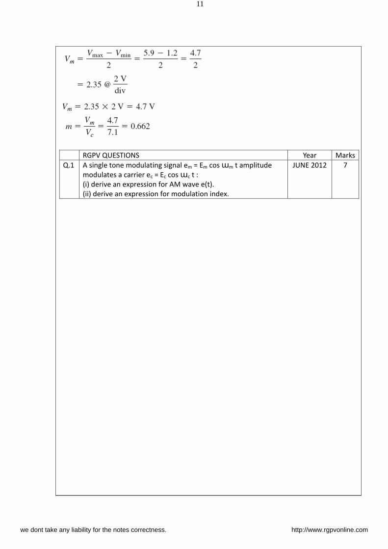
itself. When the AM signal is displayed on an oscilloscope, the modulation index can be
computed from Vmax and Vmin as shown in Fig.4. The peak value of the modulating signal is
Vm one-half the difference of the peak and trough values:
we dont take any liability for the notes correctness. http://www.rgpvonline.com

10
Fig 4:- An AM wave showing peaks (Vmax) and troughs (Vmin)
As shown in Fig., Vmax is the peak value of the signal during modulation, and Vmin is the
lowest value, or trough, of the modulated wave. The Vmax is one-half the peak-to-peak value
of the AM signal, or Vmax Vmin Vmax (p –p)/2.Subtracting Vmin from Vmax produces the
peak-to- peak value of the modulating signal. One-half of that, of course, is simply the peak
value.
The peak value of the carrier signal Vc is the average of the Vmax and Vmin and values:
The modulation index is
The modulation index or depth, of AM is more commonly expressed as the percentage of
modulation rather than as a fractional value. the percentage of modulation is 100 x m ,
Example:-
In an AM signal the Vmax (p-p) value read from the graticule on the oscilloscope screen is 5.9
divisions and Vmin( p–p) is 1.2 divisions.
a. What is the modulation index?
b. Calculate Vc, Vm, and m if the vertical scale is 2 V per division.
Solution:-
M=
we dont take any liability for the notes correctness. http://www.rgpvonline.com
11
RGPV QUESTIONS Year Marks
Q.1 A single tone modulating signal em = Em cos ɯm t amplitude
modulates a carrier ec = Ec cos ɯc t :
(i) derive an expression for AM wave e(t).
(ii) derive an expression for modulation index.
JUNE 2012 7
we dont take any liability for the notes correctness. http://www.rgpvonline.com

12
UNIT-02/LECTURE-03
POWER DISTRIBUTION
AM Voltage Distribution:- (JUNE 2010)(10)
An unmodulated carrier can be Described mathematically as
Therefore, the instantaneous amplitude of the modulated wave can be expressed as
Fig 5:-Voltage spectrum for an DSB-FC
AM Power Distribution:-
The average power dissipated in a load by an unmodulated carrier is equal to the rms carrier
voltage squared, divided by the load resistance.
Mathematically, power in an unmodulated carrier is
The upper and lower sideband powers are expressed mathematically as:
The total power in an amplitude-modulated wave is equal to the sum of the powers of the
carrier, the upper sideband, and the lower sideband:
The total power in an AM signal when the carrier power and the percentage of modulation
are known:
we dont take any liability for the notes correctness. http://www.rgpvonline.com

13
Fig 6:-Power Spectrum for an AM DSBFC wave with a single-frequency modulating signal
Note that with 100% modulation the maximum power in the upper or lower sideband
is equal to only one-fourth the power in the carrier.
Thus, the maximum total sideband power is equal to one-half the carrier power.
One of the most significant disadvantages of AM DSBFC transmission is the fact that
the information is contained in the sidebands although most of the power is wasted in
The carrier.
Actually, the power in the carrier is not totally wasted because it does allow for the
use of relatively simple, inexpensive demodulator circuits in the receiver, which is the
predominant advantage of AM DSBFC.
Example:-
A carrier Acoswct is modulated by a single tone modulating signal f(t)=Emcoswmt. Find
(a) Total modulated power
(b) RMS (root mean square ) value of the modulated signal,and
(c) Transmission efficiency for a 100 percent modulation.
Solution:-
i) Carrier power (unmodulated) Pc =mean square value of Acoswct =A2/2
Sideband power Ps= Em2/4
Total power P is the sum of Pc and Ps
Pt = Pc + Ps
Pt= A2/2 + Em
2/4
Pt= A2/2 [1 + ½ (Em/A)
2]
Putting Em/A = ma and A2/2 = Pc
Total modulated power P= Pc [1 + ½ (ma) 2
]
Where ma is the modulation index
Pt=Pc + Pc(ma) 2
/2
Where second term Pc(ma) 2
/2 is known as sideband power
ii) The rms value is under root of the ms value (power) of the AM signal
Now, by putting
we dont take any liability for the notes correctness. http://www.rgpvonline.com

14
(i) Transmission efficiency is given by
Eff =(useful power /total power) x 100
Eff =(side band power / total power) x 100
Eff =(Ps / Pt) x 100
Eff =( Pc(ma) 2
/2 / Pc [1 + ½ (ma) 2
]) x 100
Eff =[(ma) 2
/[2 + (ma) 2
] ]x 100
For a 100 percent modulation ma= 1
Eff =1 2
/[2 + 1 2
] x 100
Eff =(1 /3) x 100
Eff =33.3%
It means for a 100 percent modulation the sidebands carry only one third of the total power.
This is the maximum power which can be carried by the sidebands in AM. If ma is less than
100 percent the sideband power will be further reduced.
*****
Example:-
if the carrier of an AM transmitter is 1000 W and it is modulated 100 percent. Find the total
power and sideband power.
Solution:-
Given Pc = 1000W and ma = 1
the total AM power is Of the total power
1000 W of it is in the carrier. That leaves 500 W in both sidebands. Since the sidebands are
equal in size, each sideband has 250 W.For a 100 percent modulated AM transmitter, the total
sideband power is always one-half that of the carrier power.
Psb = 500 W
Plsb = Pusb =250
It is also calculated by formule
Plsb = Pusb = (1
2x 1000) /4 =1000/4 = 250 w
*****
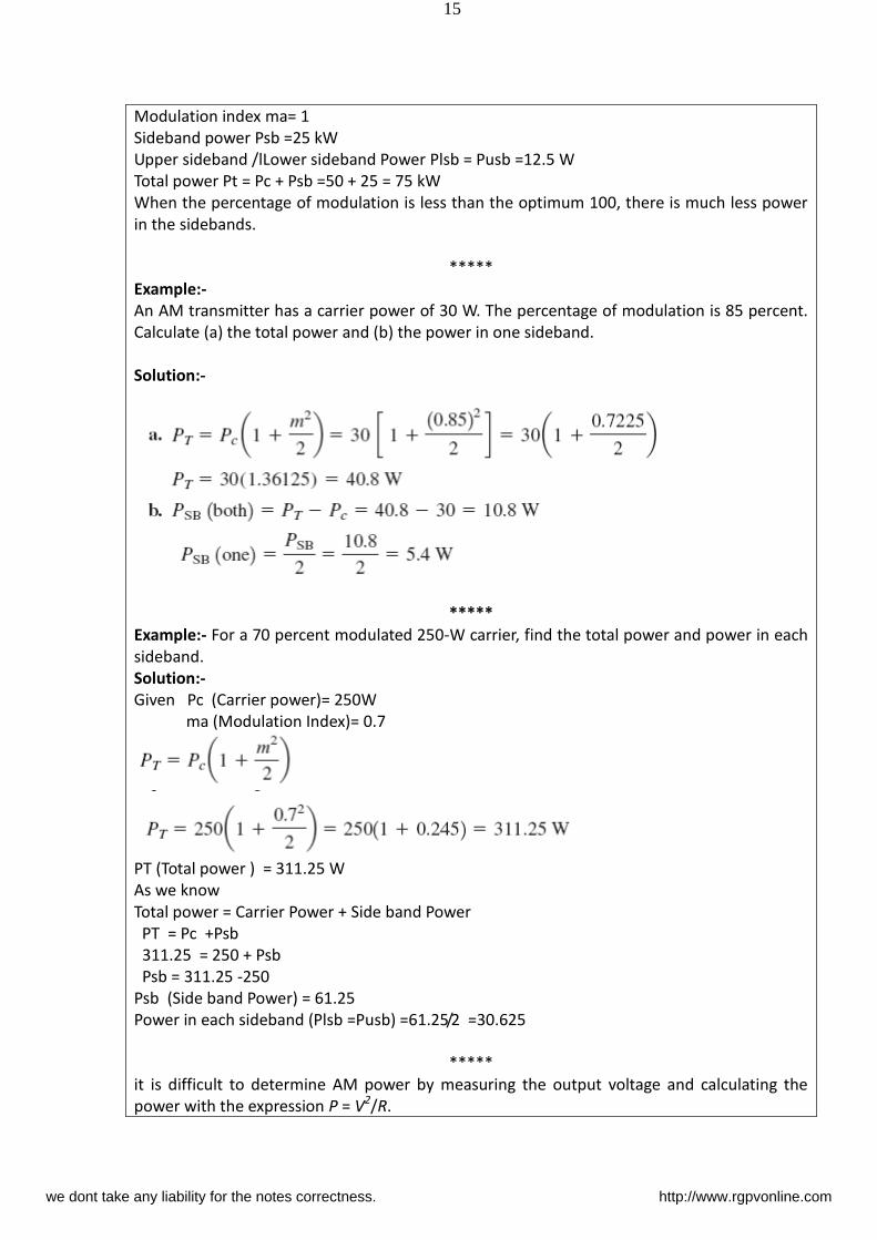
Example:- A 50-kW transmitter carrier that is 100 percent modulated will have a sideband
power of 25 kW, with 12.5 kW in each sideband. Calculate The total Power.
Solution:-
Carrier Power Pc = 50 kW
we dont take any liability for the notes correctness. http://www.rgpvonline.com
15
Modulation index ma= 1
Sideband power Psb =25 kW
Upper sideband /lLower sideband Power Plsb = Pusb =12.5 W
Total power Pt = Pc + Psb =50 + 25 = 75 kW
When the percentage of modulation is less than the optimum 100, there is much less power
in the sidebands.
*****
Example:-
An AM transmitter has a carrier power of 30 W. The percentage of modulation is 85 percent.
Calculate (a) the total power and (b) the power in one sideband.
Solution:-
*****
Example:- For a 70 percent modulated 250-W carrier, find the total power and power in each
sideband.
Solution:-
Given Pc (Carrier power)= 250W
ma (Modulation Index)= 0.7
PT (Total power ) = 311.25 W
As we know
Total power = Carrier Power + Side band Power
PT = Pc +Psb
311.25 = 250 + Psb
Psb = 311.25 -250
Psb (Side band Power) = 61.25
Power in each sideband (Plsb =Pusb) =61.25/2 =30.625
*****
it is difficult to determine AM power by measuring the output voltage and calculating the
power with the expression P = V2/R.
we dont take any liability for the notes correctness. http://www.rgpvonline.com

16
However, it is easy to measure the current in the load. For example, you can use an RF
ammeter connected in series with an antenna to observe antenna current. When the antenna
impedance is
known, the output power is easily calculated by using the formula
PT = IT 2
R
where Here Ic is the un modulated carrier current in the load, and m is
the modulation index.
Example:-
The total output power of an 85 percent modulated AM transmitter, whose unmodulated
carrier current into a antenna load impedance is 10 A. Calculate Total carrier power.
Solution:-
Given ma = 0.85
Ic = 10amp
*****
One way to find the percentage of modulation is to measure both the modulated and
the unmodulated antenna currents. Then, by algebraically rearranging the formula above,
m can be calculated directly:
Example:-
The unmodulated antenna current is 2.2 A. That is the current produced by the carrier only, or
Now, if the modulated antenna current is 2.6 A, Find the modulation index.
Solution:-
*****
we dont take any liability for the notes correctness. http://www.rgpvonline.com

17
Example:-
A a te a has a i peda e of Ω .A u odulated AM sig al p odu es a u e t
of 4.8 A. The modulation is 90 percent. Calculate
(a) the carrier power,
(b) the total power, and
(c) the sideband power.
Solution:-
*****
Example:-
The transmitter experiences an antenna current change from 4.8 A unmodulated to 5.1 A.
What is the percentage of modulation?
Solution:-
The percentage of modulation is 51.
*****
Example:-
Find total modulated power, sideband power and net modulation index for the AM signal
Solution:-
The expression can be written as
we dont take any liability for the notes correctness. http://www.rgpvonline.com

18
The signal is equivalent to the expression
Here
Unmodulated carrier power
The power of the modulated signal is given by
Sideband power
Net modulation index m is given by
*****
RGPV QUESTIONS Year Marks
Q.1 Prove that after amplitude modulation, the carrier power
increases from Pc to P Pc (1+ ma/2) where ma is the modulation
index.
JUNE 2010 10
we dont take any liability for the notes correctness. http://www.rgpvonline.com

19
UNIT-02/LECTURE-04
BALANCE/CHOPPER MODULATOR
Generation of DSB-SC:-
Chopper type balanced modulator/Ring Modulator:-
The chopper modulator The chopper modulator or ring modulator is a common type of
modulator. A diagram is shown below
Cos(wct) is a square wave. During the positive half cycle f(t) is switched on to the other side.
When Cos(wct) is 0 the waveform is switched off. The bandpass filter will remove higher
frequency components which are not needed. The corresponding waveforms are shown
below
This is a theoretical model of a chopper modulator. A popular configuration is the double-
balanced ring modulator. The modulator is popular as it does not require ideal components ,
provided that they have matched characteristics (i.e. use the same part numbers).
we dont take any liability for the notes correctness. http://www.rgpvonline.com

20
Assuming that ei(t) is 0. During the positive half cycles diodes D1 and D2 will conduct and the
point a is connected to the out put transformer secondary. If the secondary of the reference
transformer is accurately centre tapped and if the impedances of D1 and D2 are identical than
no current will flow through the output transformer and no voltage will be developed at the
output. During the next half cycle D3 and D4 conduct and point b is connected to the input
through the opposite half cycle of the output transformer secondary. Again no current will
flow and no output will result. Thus we see that the carrier is suppressed.
Now let ei(t) have the modulating input. Let us apply a positive polarity input signal whose
peak amplitude is much smaller than that of the reference eR. On the positive half-cycles of
Coswct, point a is essentially at ground potential and a current will flow upward through half
of the output transformer secondary, inducing a positive output voltage. On the negative half-
cycles of Coswct, point b is essentially at ground potential and a current will flow downward
through the opposite half of the output transformer secondary, inducing a negative output
voltage.
The peak positive and negative output voltages will be identical for a given fixed signal
amplitude if the output transformer is accurately centre tapped. Therefore we have
developed a signal that alternates in sign at a rate determined by the carrier frequency and
whose amplitude is proportional to the input signal amplitude. For DSB-SC modulation to
occur
In practice, an imbalance between diode characteristics and inaccuracies in the transformer
centre taps will result in non-ideal performance and carrier leakage. Balancing controls can be
added to fully tune out carrier leakage.
Non linear devices:-
Balanced Modulator:- (DEC 2013)(7)
Amplitude modulation can also arise in non linear systems. Diodes are good examples of non
linear devices and may be used as a modulator. The following balanced modulator uses non
linear devices to generate a DSB-SC AM.
we dont take any liability for the notes correctness. http://www.rgpvonline.com

21
The non linearity can be approximated by the following power series
Referring to the above figure. By the transformer actions
Retaining up to the power of the current than becomes
For a resistive load the net voltage is [i1(t) –i2(t)]R the output is
The output at the BPF centered around Wc is given by
eo(t) = 4aRf(t) Coswct
eo(t) = k f(t) Coswct
this is the desired expression for AM-SC or DSB-SC
RGPV QUESTIONS Year Marks
Q.1 Write short note on balanced modulator. DEC 2013 7
Q.2 With the help of a circuit diagram, explain the working of
Balance Modulator for DSB-SC generation.
DEC 2010 10
we dont take any liability for the notes correctness. http://www.rgpvonline.com

22
UNIT-02/LECTURE-05
SSB GENERATOR (PHASE AND FREQUENCY DISCRIMINATION METHOD),VSB TRANSMISSION
Single Side Band (SSB) Modulation:-
In DSB-SC it is observed that there is symmetry in the band structure. So, even if one half is
transmitted, the other half can be recovered at the received. By doing so, the bandwidth and
power of transmission is reduced by half. Depending on which half of DSB-SC signal is
transmitted,
there are two types of SSB modulation
1. Lower Side Band (LSB) Modulation
2. Upper Side Band (USB) Modulation
Fig 12:- SSB signals from original signal
we dont take any liability for the notes correctness. http://www.rgpvonline.com
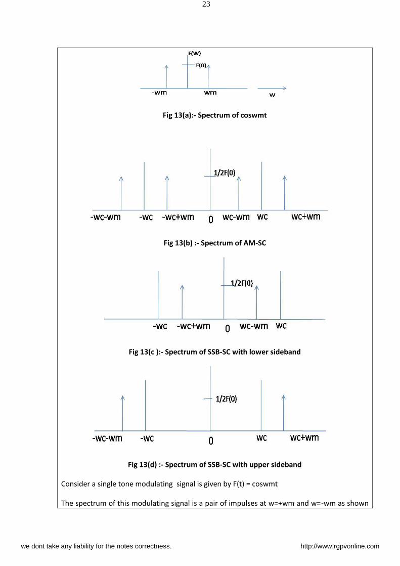
23
Fig 13(a):- Spectrum of coswmt
Fig 13(b) :- Spectrum of AM-SC
Fig 13(c ):- Spectrum of SSB-SC with lower sideband
Fig 13(d) :- Spectrum of SSB-SC with upper sideband
Consider a single tone modulating signal is given by F(t) = coswmt
The spectrum of this modulating signal is a pair of impulses at w=+wm and w=-wm as shown
we dont take any liability for the notes correctness. http://www.rgpvonline.com

24
in above fig (a) .let this signal modulate a carrier coswct, the resulting AM-SC (DSB-SC)
spectrum is shown in (b) . in order to get the SSB-SC waveform ,one of the sideband is
eliminated. Fig (c) represented the spectrum of SSb-SC with lower sidebands. It is obvious
from the spectrum that this corresponds to a time domain signal cos (wc-wm)t, since the
spectrum of cosine function consists of two impulses in its frequency domain. thus the SSb-SC
(lower sideband) signal may be expressed as
cos(wc- t = os t os t + si t si t ………….. i
similarly.yhe expression for the single tone SSB-SC with upper sidebands (fig:d) may be given
as
cos(wc +wm)t = coswmt coswct - si t si t ……………. ii
equation (i) and (ii) may be combined to be written as
Ф ss t = os t os t + - )sinwmt sinwct …………. iii
Where (+ ) sign indicated the lower sideband and ( - ) sign indicates the upper sideband.
The terms sinwmt and sinwct may be written as
sinwmt = cos (wmt – π/ ……………… i
sinwct = cos (wct – π/ ………………
thus, the sine terms can be obtained from the corresponding terms, by giving a phase shift of
( - π/ . E uatio (iii) is an expression for SSB-SC for a specific case of single tone modulation.
In equation (iii) the term sinwmt is obtained by giving a phase shift of (- π/ to the modulating frequency coswmt.
Similarly, in a general modulating signal f(t) ,if all the frequency components are shifted by
(- π/ , it a lead to a SSB-SC signal.
Thus equation (iii) may be extended for a SSB-SC signal modulated by a general modulating
signal f(t) as given below:
Ф ss t = f t os t + - ) fh(t) sinwct ……………. i
Where fh(t) is a signal obtained by shifting the phase of every component present in f(t) by
( - π/ . Si ila l e uatio iii + sig i di ated the lo e side a d a d - ) sign indicates
the upper sideband.
we dont take any liability for the notes correctness. http://www.rgpvonline.com

25
There are two methods used for SSB Transmission:-
1. Filter Method
2. Phase Shift Method
Filter Method/frequency discrimination method:-
This is the filter method of SSB suppression for the transmission. Fig
illustrates the block diagram of this method.
1. A crystal controlled master oscillator produces a stable carrier frequency fc (say 100
KHz)
2. This carrier frequency is then fed to the balanced modulator through a buffer
amplifier which isolates these two satges.
3. The audio signal from the modulating amplifier modulates the carrier in the balanced
modulator. Audio frequency range is 300 to 2800 Hz. The carrier is also suppressed in
this stage but allows only to pass the both side bands. (USB & LSB).
4. A band pass filter (BPF) allows only a single band either USB or LSB to pass through it.
It depends on our requirements.
Let we want to pass the USB then LSB will be suppressed. Inthis case.
fc = 100 KHz
Audio range = 300 - 2800 Hz
USB frequency range = fc + 300 to fc + 2800
= 100000 + 300 to 100000 + 2800
= 100300 to 102800 Hz
So this band of frequency will be passed on through the USB filter section
5. This side band is then heterodyned in the balanced mixer stage with 12 MHz
frequency produced by crystal oscillator or synthesizer depends upon the
requirements of our transmission. So in mixer stage, the frequency of the crystal
oscillator or synthersizer is added to SSB signal. The output frequency thus being
raised to the value desired for transmission.
6. Then this band is amplified in driver and power amplifier stages and then fed to the
aerial for the transmission.
Advantages:- The advantages of single side band SSB transmission are as follows.
1. It allows better management of the frequency spectrum. More transmission can fit
we dont take any liability for the notes correctness. http://www.rgpvonline.com

26
into a given frequency range than would be possible with double side band DSB
signals.
2. All of the transmitted power is message power none is dissipate as carrier power.
3. The noise content of a signal is an exponential function of the bandwidth: the noise
will decrease by 3dB when the bandwidth is reduced by half. There fore, single side
band SSB signals have less noise contamination than DSB double side band.
Disadvantages:-
1. The cost of a single side band SSB reciver is higher than the double side band DSB
counterpart be a ratio of about 3:1.
2. The average radio user wants only to flip a power switch and dial a station. Single side
band SSB recievers require several precise frequency control settings to minimize
distortion and may require continual readjustment during the use of the system.
Phase Shift Method/phase discrimination method:- (DEC 2012)(7)
The phaseing method of SSB generation uses a phase shift technique that causes one of the
side bands to be conceled out. A block diagram of a phasing type SSB generator is shown in
fig.
1. It uses two balanced modulators instead of one. The balanced modulators effectively
eliminate the carrier. The carrier oscillator is applied directly to the upper balanced
modulator along with the audio modulating signal. Then both the carrier and
modulating signal are shifted in phase by 90o and applied to the second, lower,
balanced modulator. The two balanced modulator output are then added together
algebraically. The phase shifting action causes one side band to be canceled out when
the two balanced modulator outputs are combined.
2. The carrier signal is VcSi πfct the modulating signal is VmSi πfmt. Balanced
modualtor produces the product of these two signals.
(VmSi πfmt)(VcSi πfct)
Applying a trignometric identity.
(VmSi πfmt)(VcSi πfct = / [Cos πfc - πfm)t - Cos πfc + πfm)t]
Note that these are the sum and diffrence frequencies or the upper and lower side
bands.
It is important to remember that a cosine wave is simply a sine wave shifted by 90o A cosine
we dont take any liability for the notes correctness. http://www.rgpvonline.com

27
wave has exactly the same shape as a sine wave, but it occurs 90o
The 90o phase shifters create cosine waves of the carrier and modulating signal whichare
multiplied in balanced modulator to produce
(Vm - Cos πfmt)(VcCos πfct)
(Vm - Cos πfmt)(VcCos πfct)
Another common trigonometric identity translates this to
(VmCos πfmt)(VcCos πfct = / [Cos πfc - πfm t + Cos πfc + πfm)t]
Now if you add these two expressions together the sum frequencies cancel while the
difference frequencies add producing only the lower side band:
Cos πfc - πfm)t
Vestigial Side Band (VSB) Modulation:- (DEC 2013)(7)
The following are the drawbacks of SSB signal generation:
1. Generation of an SSB signal is difficult.
2. Selective filtering is to be done to get the original signal back.
3. Phase shifter should be exactly tuned to 900.
To overcome these drawbacks, VSB modulation is used. It can viewed as a compromise
between SSB and DSB-SC. Figure 14 shows all the three modulation schemes.
Figure 14: VSB Modulation
In VSB
1. One sideband is not rejected fully.
2. One sideband is transmitted fully and a small part (vestige)
of the other sideband is transmitted.
The transmission BW is BW= B + v. where, v is the vestigial frequency band.
The generation of VSB signal is shown in Figure 15
Figure 15: Block Diagram - Generation of VSB signal
we dont take any liability for the notes correctness. http://www.rgpvonline.com

28
Here, Hi(w) is a filter which shapes the other sideband.
ФVSB(w) = [M(w -wc) +M(w + wc)] Hi(w)
To recover the original signal from the VSB signal, the VSB
Signal is multiplied with cos(wct) and passed through an LPF such that original signal is
recovered.
Figure 16: Block Diagram - Demodulation of VSB signal
From Figure 15 and Figure16, the criterion to choose LPF is:
M(w = [ФVSB(w + wc + ФVSB(w-wc)] H0(w)
= [Hi(w + wc) + Hi(w-wc)] .M(w).H0(w)
Application:-
Vestigial SideBand. It is a type of signal modulation (filtering) used in the television
communication industry. It is used to help remove signal redundancy in Pulse Amplitude
Modulated (PAM) signals.
RGPV QUESTIONS Year Marks
Q.1 Explain about VSB transmission in detail? DEC 2013
DEC 2012
7
7
Q.2 Explain the phase discrimination method for generating SSB
signals.
DEC-2012 7
we dont take any liability for the notes correctness. http://www.rgpvonline.com

29
UNIT-02/LECTURE-06
DETECTION OF AM SIGNALS
Demodulation of AM waves:-
There are two methods to demodulate AM signals. They are:
Square-law detector
Envelope detector
Square-law detector:-
A Square-law modulator requires nonlinear element and a low pass filter for extracting the
desired message signal. Semi-conductor diodes and transistors are the most common
nonlinear devices used for implementing square law modulators. The filtering requirement is
usually satisfied by using a single or double tuned filters.
When a nonlinear element such as a diode is suitably biased and operated in a restricted
portion of its characteristic curve, that is ,the signal applied to the diode is relatively weak, we
find that transfer characteristic of diode-load resistor combination can be represented closely
by a square law :
V0 (t) = a1Vi (t) + a2 Vi2 t ………………. i
Where a1, a2 are constants
Now, the input voltage Vi (t) is the sum of both carrier and message signals
i.e., Vi (t) = Ac [1+kam (t)] os πf t ……………. ii
Substitute equation (ii) in equation (i) we get
V t = a A [ +ka t ] os πf t + / a A 2 [1+2 kam (t) + ka
2m
2 t ] os πf t]……….. iii
Now design the low pass filter with cutoff frequency f is equal to the required message signal
bandwidth. We can remove the unwanted terms by passing this output voltage V0 (t) through
the low pass filter and finally we will get required message signal.
V0 (t) = Ac2
a2 m (t)
The Fourier transform of output voltage VO (t) is given by
VO (f) = Ac2 a2 M (f)
Fig 17:- Spectrum of output signal
we dont take any liability for the notes correctness. http://www.rgpvonline.com

30
Envelope Detector:- (DEC 2013)(7)
Fig 18:- Envelope Detector
Envelope detector is used to detect high level modulated levels, whereas square-law detector
is used to detect low level modulated signals (i.e., below 1v). It is also based on the switching
action or switching characteristics of a diode. It consists of a diode and a resistor-capacitor
filter.
The operation of the envelope detector is as follows. On a positive half cycle of the input
signal, the diode is forward biased and the capacitor C charges up rapidly to the peak value of
the input signal. When the input signal falls below this value, the diode becomes reverse
biased and the capacitor C discharges slowly through the load resistor Rl . The discharging
process continues until the next positive half cycle. When the input signal becomes greater
than the voltage across the capacitor, the diode conducts again and the process is repeated.
The charging time constant RsC is very small when compared to the carrier period 1/fc i.e.,
RsC << 1/fc
Where Rs = internal resistance of the voltage source.
C = capacitor
fc = carrier frequency
i.e., the capacitor C charges rapidly to the peak value of the signal. The discharging time
constant RC is very large when compared to the charging time constant i.e.,
1/fc << RC << 1/W
Where R = load resistance value
W = message signal bandwidth
i.e., the capacitor discharges slowly through the load resistor.
RGPV QUESTIONS Year Marks
Q.1 Explain envelope detector with the help of suitable circuit
diagram.
DEC 2013 7
we dont take any liability for the notes correctness. http://www.rgpvonline.com

31
UNIT-02/LECTURE-07
SYNCHRONOUS DETECTION TECHNIQUE,ERROR IN SYNCHCRONOUS DETECTION
Synchronous detection:- (JUNE 2013)(7)
The AM-SC system is used at the transmitter for shifting the baseband signal (with maximum
frequency wm) to a higher carrier frequency (+-wc). This modulated signal is transmitted from
the transmitter and it reaches the receiver via a propagating media. At the receiver, the
original baseband signal f (t) is desired to be recovered from the modulated signal. This is
achieved by retranslating the baseband signal from a higher spectrum (centered around +-
wc) to the original spectrum. This process of retranslation is known as demodulation or
detection. The original baseband is recovered from the modulated signal by the detection
process.
A method for detecting the AM-SC signal shown in fig 20 (a),is used at the receiver end for
recovery of the message signal.
Fig 20 (a): Block Diagram
The method of retranslation is similar to that of translation. Here modulated signal f(t) coswct
is multiplied with coswct and passed through a low pass filter. The signal f(t) coswct when
multiplied with coswct. Yields
f(t) coswct coswct = f(t)cos2wct
= ½ f(t) [1+cos2wct]
= ½ f t + ½ f t os t ……………………. i
It is clear from right hand side of equation (i) that the term ½ f(t) cos2wct centered around (+-
2wc) can be bypassed by a low pass filter, and at the output of the low pass filter original
baseband signal ½ f(t) is recovered. The spectrum of f(t)cos2wct is obtained by taking Fourier
transform of RHS of equation (i)
f(t)cos2wct ½ F(w) + ¼ [ F (w+2wc) + F(w- ] ……………… ii
Fig 20 (b):Spectrum of f(t) coswct
we dont take any liability for the notes correctness. http://www.rgpvonline.com

32
The spectrum is shown in fig(b). The spectrum reveals that the original baseband signal (0 to
wm) is present along with another spectrum centered around (+-2wc).when passed through a
low pass filter (with a cutoff frequency wm), the original baseband signal appears at the
output of the filter. The spectrum centered near (+-2wc) is not allowed to pass through low
pass filter. Note that wc >> wm and 2wc is still greater than wm, and is easily filtered out.
Thus the original message signal f(t) is recovered from AM-SC signal .
Effect of Phase and frequency errors in synchronous detection:-
The frequency and phase of the local oscillator signal in synchronous detection must be
identical to the transmitted carrier. Any discrepancy in frequency and/or phase causes a
distortion in the detected output at the receiver. Let us examine the nature of distortion
Caused by phase or frequency discrepancy.
Let a modulated signal reaching the receiver the receiver signal be f(t) coswct. Assuming, a
locally generated signal with frequency and phase e o e ual to ∆ a d φ espe ti el , the product of the two signals in the synchronous detector yields,
ed t =f t os t . os [ + ∆ t + φ] = ½ f t { os[ ∆ t+ φ]+ os [ + ∆ t + φ]} ……………… iii
When this signal is passed through a low pass filter with a cut off frequency wm,the terms
centered around (+-2wc) are filtered out and the filter output is given by
eo t = ½ f t os [ ∆ t + φ] ………… i
the baseband sig al f t is ultiplied a slo ti e a i g fu tio os [ ∆ t + φ] that distorts the message signal f(t). let us consider the following special cases,
(i) Whe the f e ue e o ∆ a d phase e o φ a e oth ze o
∆ = , φ=
Equation (iv) yields,
eo(t) = ½ f(t)
i.e. there is no distortion in the detected output
(ii) Whe the e is o l the phase e o φ , ∆ = , φ ≠
i.e. then equation (iv) becomes
eo t = ½ f t os φ hi h sho s that output is ultiplied of os φ . he φ is ti e i depe de t, the e is o
disto tio , athe the e is o l atte uatio . the output is a i u he φ = , a d i i u he φ =9 ’.
Quadarature Null Effect:-
The detected output is zero when φ=9 ’.this is called a quadarature null effect, because the
signal is zero when the local carrier is in phase quadrature with the transmitted carrier.
(iii) Whe the e is o l the F e ue e o ∆ , ∆ ≠ , φ =
i.e. then equation (iv) becomes
eo t = ½ f t os ∆ t
He e the ultipl i g fa to os ∆ t is ti e depe de t a d auses disto tio i the
we dont take any liability for the notes correctness. http://www.rgpvonline.com
33
dete ted output. the e o ∆ is usually small, and hence a message f(t) is multiplied by a
slow varying sinusoidal signal. This is a more serious distortion. Hence frequency error should
be avoided.
(iv) When both errors are non-zero
∆ ≠ , φ ≠ , Equation (iv) itself provides the detected output. In this case,the constant phase error
provides attenuation and the frequency error causes distortion in the detected output. thus
we get an attenuated and distorted output in the receiver.
RGPV QUESTIONS Year Marks
Q.1 Explain the synchronous detection method of DSB-SC signals.
Explain the effect of phase and frequency errors in
synchronous detection.
JUNE 2013
DEC 2011
7
10
we dont take any liability for the notes correctness. http://www.rgpvonline.com

34
UNIT-02/LECTURE-08
ANGLE MODULATION
Angle modulation:- (JUNE 2013)(7)
Angle modulation is a method of analog modulation in which either the phase or frequency
of the carrier wave is varied according to the message signal. In this method of modulation
the amplitude of the carrier wave is maintained constant. Let us consider an unmodulated carrier wave is given by
Where A is the amplitude of the carrier wave and = I s the total phase angle of the carrier
= By differentiating the we get,the costant angular velocity
is constant with time for an unmodulated carrier, but in general this derivative may not
be constant with time, rather it may vary with time.
This time dependent angular velocity is called instantaneous angular velocity and denoted by
Where is time dependent
Types of Angle Modulation:-
There are two commonly used methods of angle modulation:
1. Frequency Modulation, and
2. Phase Modulation
An important feature of FM and PM is that they can provide much better protection to the
message against the channel noise as compared to the linear (amplitude) modulation
schemes. Also, because of their constant amplitude nature, they can withstand nonlinear
distortion and amplitude fading. The price paid to achieve these benefits is the increased
bandwidth requirement; that is, the transmission bandwidth of the FM or PM signal with
constant amplitude and which can provide noise immunity is much larger than 2W , where W
is the highest frequency component present in the message spectrum.
Phase Modulation (PM):-
In this type of angle modulation the phase angle is varied linearly with a modulating
signal f(t) about an unmodulated carrier . the instantaneous value of phase angle is
we dont take any liability for the notes correctness. http://www.rgpvonline.com
35
equal to the phase of an unmodulated carrier plus a time varying component
proportional to f(t)
Note that is time independent and hence has been ignored where kp is the phase sensitivity of the modulator in radians per volt.
Thus the phase modulated signal is defined as
Frequency Modulation (FM):- In frequency modulation the instantaneous frequency is varied linearly with message
signal, f(t) as:
where kf is the frequency sensitivity of the modulator in hertz per volt.
The total phase angle of the FM wave can be obtained by
and thus the frequency modulated signal is given by
If we assume that the phase angle of the carrier at t=0 is zero, then the limit of integration will
be 0 to t, represented by
we dont take any liability for the notes correctness. http://www.rgpvonline.com
36
Fig (1):-PM and FM waveforms with a message signal
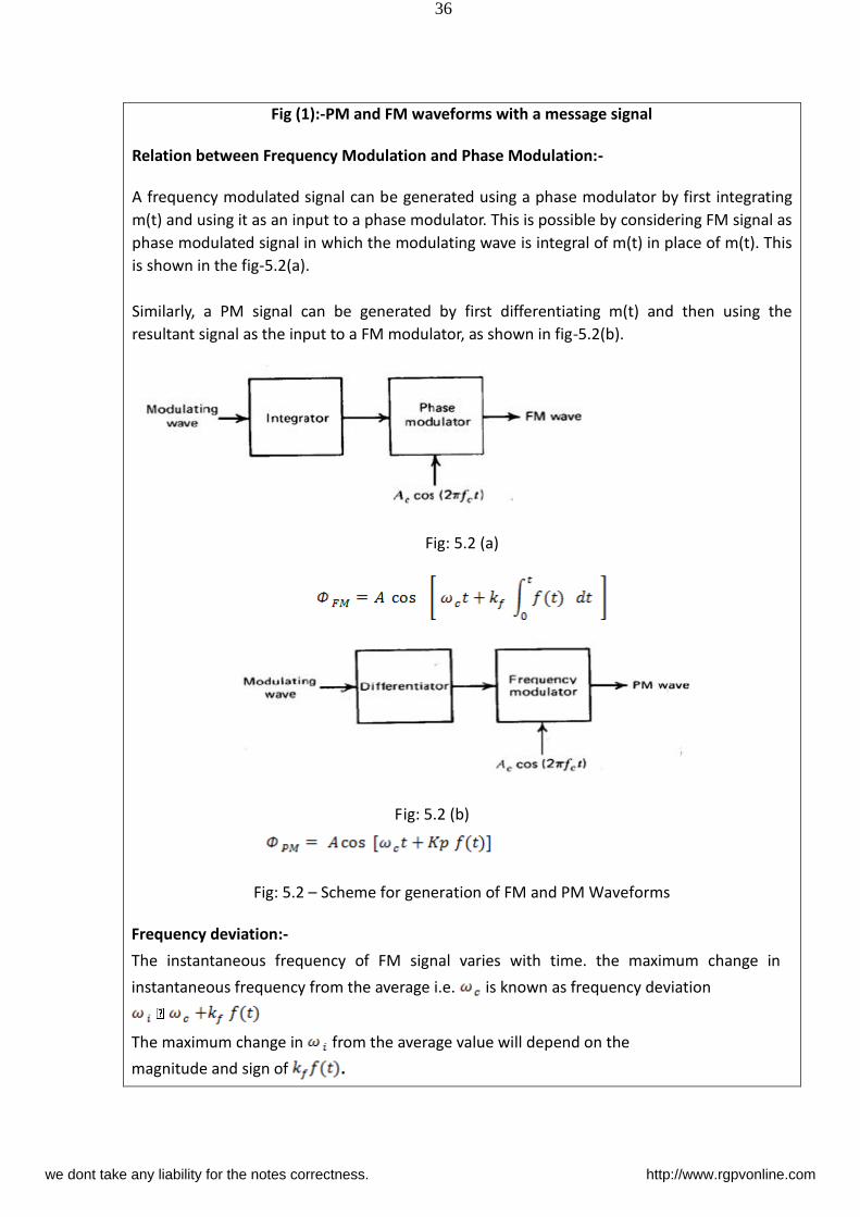
Relation between Frequency Modulation and Phase Modulation:-
A frequency modulated signal can be generated using a phase modulator by first integrating
m(t) and using it as an input to a phase modulator. This is possible by considering FM signal as
phase modulated signal in which the modulating wave is integral of m(t) in place of m(t). This
is shown in the fig-5.2(a).
Similarly, a PM signal can be generated by first differentiating m(t) and then using the
resultant signal as the input to a FM modulator, as shown in fig-5.2(b).
Fig: 5.2 (a)
Fig: 5.2 (b)
Fig: 5.2 – Scheme for generation of FM and PM Waveforms
Frequency deviation:-
The instantaneous frequency of FM signal varies with time. the maximum change in
instantaneous frequency from the average i.e. is known as frequency deviation
The maximum change in from the average value will depend on the
magnitude and sign of .
we dont take any liability for the notes correctness. http://www.rgpvonline.com

37
The frequency deviation denoted by will be either positive or
negative depending on the sign of .
Example:-
A single tone modulating signal frequency modulates a carrier
,Find the frequency deviation.
Solution:-
The deviation
Hence the maximum magnitude of ,the deviation is
And the frequency sensitivity is
radian per volt
Types of frequency modulation:-
The bandwidth of an FM signal depends on the deviation . When the deviation is
high,the bandwidth will be large ,and vice versa.
Thus for a given f(t) ,the deviation and hence bandwidth will depend on frequency
sensitivity .
If is too small then the bandwidth will be narrow and vice versa. thus depending on the
value of ,we can divide FM in to two categories,
(i) Narrowband FM (NBFM) :- When is small the bandwidth of FM is narrow. The
bandwidth of a narrow band FM is same as that of AM, which is twice the baseband.
(ii) Wideband FM (WBFM) :- When has an appreciable value, then the FM signal has a
wide bandwidth. The bandwidth of a wideband FM is too large; ideally infinite
RGPV QUESTIONS Year Marks
Q.1 What is angle modulation? How FM signal can be generated
with PM signal? Discuss in detail
JUNE 2013 7
we dont take any liability for the notes correctness. http://www.rgpvonline.com
38
UNIT-02/LECTURE-09
NARROWBAND FM AND WIDEBAND FM
NARROWBAND FM:- (JUNE 2013)(7)
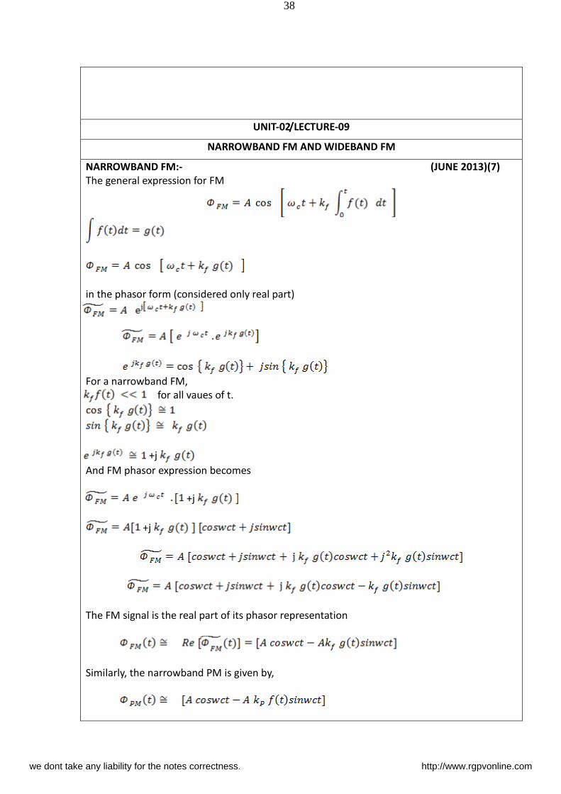
The general expression for FM
in the phasor form (considered only real part)
For a narrowband FM,
for all vaues of t.
+j
And FM phasor expression becomes
+j
+j
The FM signal is the real part of its phasor representation
Similarly, the narrowband PM is given by,
we dont take any liability for the notes correctness. http://www.rgpvonline.com

39
The expression for FM and PM are very much similar to the expression of the AM signal, with
only a slight modification.
Hence, the bandwidth of narrowband FM is same as that of the AM. it can be seen that g(t)
and f(t) have the same bandwidth.
Example :-
A carrier is frequency modulated by a single tone modulating signal
. find
(a) An expression for FM wave,and
(b) An expression for a narrowband FM.
Solution:
(a) The modulating signal is given by
The instantaneous frequency of the resulting modulated signal can be obtained
We find that ,the frequency deviation
The phase angle of the modulated wave is obtained by integrating
The term is known as the modulation index of the FM wave. it is defined as the ratio of
frequency deviation to the modulating frequency
The FM signal is given by
This is the expression for a single tone Fm.
The maximum change in total phase angle from the centre phase is known as
phase deviation,in FM denoted by .
Thus a phase deviation equal to is produced in FM.
we dont take any liability for the notes correctness. http://www.rgpvonline.com
40
The modulation index decides whether an FM wave is narrowband or a
wideband because it is directly proportional to frequency deviation .
it is the transition point between a narrowband and wideband FM.
If then FM is a narrowband, otherwise it is a wideband.
(b) The narrowband FM is defined as
By substituting the value of g(t) in the expression of FM,we get
Since
so
This is the desired expression for a narrowband single tone FM.
*******
WIDEBAND FM:- (JUNE 2012)(7)
When is large ,the FM produces a large number of sidebands and the bandwidth of FM is
quite large. such systems are called wideband FM.
Example :-
A sinusoidal wave of amplitude 10volts and frequency of 1 kHz is applied to an FM generator
that has a frequency sensitivity constant of 40 Hz/volt. Determine the frequency deviation
and modulating index.
Solution:
Message signal amplitude Am = 10 volts
Frequency fm = 1000 Hz
frequency sensitivity k f = 40 Hz/volt
Frequency deviation
we dont take any liability for the notes correctness. http://www.rgpvonline.com
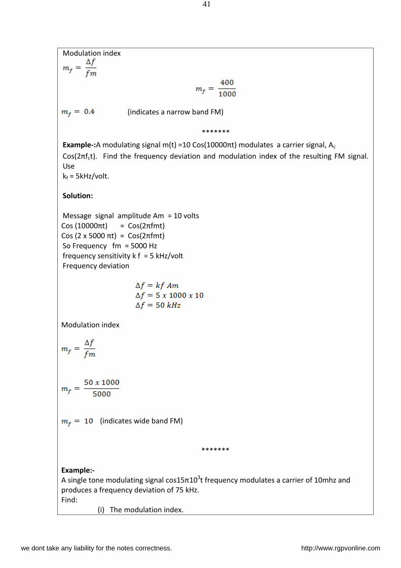
41
Modulation index
(indicates a narrow band FM)
*******
Example-:A modulating signal m(t) =10 Cos(10000πt) modulates a carrier signal, Ac Cos(2πfct). Find the frequency deviation and modulation index of the resulting FM signal.
Use
kf = 5kHz/volt.
Solution:
Message signal amplitude Am = 10 volts
Cos (10000πt) = Cos(2πf t)
Cos (2 x 5000 πt) = Cos(2πf t)
So Frequency fm = 5000 Hz
frequency sensitivity k f = 5 kHz/volt
Frequency deviation
Modulation index
(indicates wide band FM)
*******
Example:-
A si gle to e odulati g sig al os π103t frequency modulates a carrier of 10mhz and
produces a frequency deviation of 75 kHz.
Find:
(i) The modulation index.
we dont take any liability for the notes correctness. http://www.rgpvonline.com

42
(ii) Phase deviation produced in the fm wave.
(iii) if another modulating signal produces a modulation index of 100 while
maintaining the same deviation,find the frequency and amplitude of the
modulating signal assume kf = 15 khz per volt.
Solution:-
Given = 75 kHz
Cos ( π 3t) = Cos(2πf t)
π 3 = 2πf
So Frequency
(i) The modulation index.
(ii) Phase deviation produced in the fm wave.
The phase deviation in FM is equal to the modulation index
(iii)
If mf = 100 and = 75kHz
Now
As we know
******
RGPV QUESTIONS Year Marks
Q.1 What do you mean by FM? Derive an expression for NBFM? JUNE 2013
DEC 2012
7
7
Q.2 Discuss the effect of variation in mf on the spectrum of FM JUNE 2012 7
we dont take any liability for the notes correctness. http://www.rgpvonline.com

43
wave. Also explain NBFM and WBFM.
Q.3 Derive the expression of wide band FM (WBFM). DEC 2011 10
Q.4 Derive the expression for FM & NBFM along with phasor
diagram.
DEC 2010 10
UNIT-02/LECTURE-10
Transmission Bandwidth of FM waves:-
An FM wave consists of infinite number of side bands so that the bandwidth is theoretically
infinite. But, in practice, the FM wave is effectively limited to a finite number of side band
frequencies compatible with a small amount of distortion.
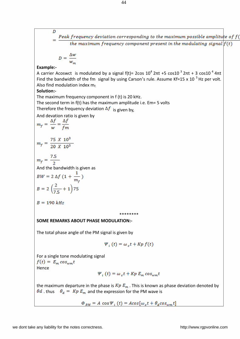
Carson’s Rule:-
An empirical formula for the bandwidth of a single tone wideband FM is given by carson’s
rule. According to this rule, the Fm bandwidth is given by
Since
So
radians
Or
Hz
(i) When
(narrowband FM) i.e.
Then
Which is equivalent to AM
(ii) When
(wideband FM) i.e.
Then
DEVIATION RATIO:-
we dont take any liability for the notes correctness. http://www.rgpvonline.com
44
Example:-
A carrier Acoswct is modulated by a signal f(t)= 2cos 104 πt + os 3 πt + os 4 πt
Find the bandwidth of the fm signal by using Carson’s rule. Assume Kf=15 x 10 3
Hz per volt.
Also find modulation index mf.
Solution:-
The maximum frequency component in f (t) is 20 kHz.
The second term in f(t) has the maximum amplitude i.e. Em= 5 volts
Therefore the frequency deviation is given by,
And devation ratio is given by
And the bandwidth is given as
********
SOME REMARKS ABOUT PHASE MODULATION:-
The total phase angle of the PM signal is given by
For a single tone modulating signal
Hence
the maximum departure in the phase is . This is known as phase deviation denoted by
. thus and the expression for the PM wave is
we dont take any liability for the notes correctness. http://www.rgpvonline.com

45
The instantaneous frequency corresponding to is given by
The maximum departure in the frequency from is .Therefore ,a frequency
deviation produced in PM is given as
Which is independent on the modulating frequency .
The frequency deviation in FM is,
.
There fore,for an equivalent bandwidth in PM and FM
BANDWIDTH OF PM:-
The PM bandwidth is given by carson’s rule
The phase modulatin index is the same as the deviation and is given by
Example:-
A odulati g sig al os π15x103t,angle modulates carrier A coswct:
(i) Find the modulation index and the bandwidth for fm and pm system.
(ii) Determine the change in the bandwidth and the modulation index for both fm and pm ,if
fm is reduced to 5 kHz.
Solution:-
Given Am =5 , fm = 15 kHz
I)
FM system
Frequency deviation
Assume = = 15 kHz/volt
So
Therefore, modulation index
we dont take any liability for the notes correctness. http://www.rgpvonline.com

46
PM system
Frequency deviation
modulation index
Corresponding band width
since is so much greater than fm
The band width is quite large as compared to FM.this is because the Modulation index in PM
is quite large
(i) Now, if fm = 5kHz
For FM: The deviation is independent of fm, and remains 75 KHz.
Thus in FM the modulation index changes considerably with a change in the modulating
frequency, but the bandwidth changes only slightly.
For PM:
Deviation is dependent on fm and is given by
Hence
since is so much greater than fm
we dont take any liability for the notes correctness. http://www.rgpvonline.com

47
The modulation index is independent of fm,so
*******
we dont take any liability for the notes correctness. http://www.rgpvonline.com