1 soi bicmos an emerging mixed-signal technology platform tak h. ning
Post on 18-Dec-2015
217 views
TRANSCRIPT

1
Thomas J. Watson Research CenterPO Box 218Yorktown Heights, NY 10598
SOI BiCMOS an Emerging Mixed-Signal
Technology Platform
Tak H. Ning

2
Outline
• Evolution of Silicon Technology
• CMOS for Mixed Signal -- Why and Why Not?
• Why SOI BiCMOS for Mixed Signal?
• Some Recent Developments
• Summary
3
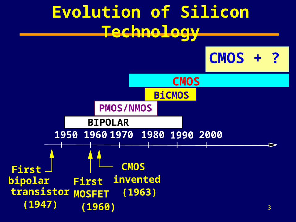
1950 19701960 19901980 2000
First bipolar transistor (1947)
First MOSFET (1960)
CMOSinvented (1963)
BIPOLAR
PMOS/NMOS
CMOSBiCMOS
CMOS + ?
Evolution of Silicon Technology

4
What Happened to BiCMOS?
• Previous BiCMOS aimed primarily for digital applications– CMOS was low power but very slow – Digital BiCMOS goal was to add bipolar to
speed up CMOS circuits– PENTIUM 1 was BiCMOS!
• CMOS speed improved by scaling– Need for digital BiCMOS disappeared by
early 1990’s

51997 1998 1999 2000 2001 2002 2003 2004 20050
200
400
600
800
1000
1200
1400
Interactive Set-Top-BoxMobile Handset
PC
Millions of devices
Source: Gartner Dataquest (November 2000 Estimates)
Devices Capable of e-Commerce Worldwide
Technology required: computing + communication

6
Channel length
Gate oxide
source drain
gate
High-Speed CMOS Trends
• Power supply voltage ~ 1 V
• Gate oxide thickness ~ 1 nm
• Short channel length but high off current
• Not suitable for many analog applications
7
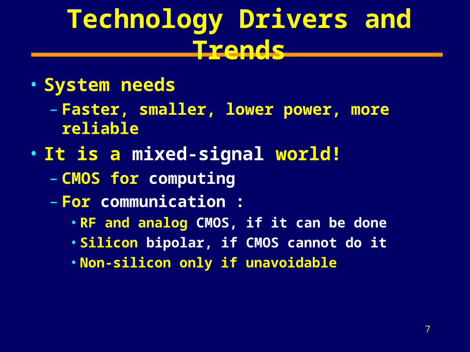
Technology Drivers and Trends
• System needs– Faster, smaller, lower power, more reliable
• It is a mixed-signal world!– CMOS for computing – For communication :
• RF and analog CMOS, if it can be done• Silicon bipolar, if CMOS cannot do it• Non-silicon only if unavoidable

8
Vds
Ids
Vgs1
Vgs2
Vgs3
Vgs4
VBE
Col
lect
or c
urre
ntIB1
IB2
IB3
IB4
IB5
Typical MOSFET Typical bipolar
Bipolar is preferred
Analog Transistors

9
Why BiCMOS?
• Systems need– CMOS for high density and low power
digital functions– Bipolar for RF and analog functions
• Integration for better systems– Faster, smaller, lower power, more reliable
• Status:– ALL major semiconductor companies either
shipping or developing BiCMOS

10
Why Not BiCMOS?
• Cost, Cost, and Cost– Process complexity– Need to evaluate cost versus benefit
• Circuit design challenges:– CMOS voltages scale (up to a point)– Bipolar voltages do not scale

11
Why SOI BiCMOS?
• SOI CMOS is here; bipolar is needed
• Isolation– Devices automatically isolated from one
another– Reduced substrate-coupling noise
• Cost?– SOI wafer cost adder– Cost saving associated with isolation
• Opportunities for innovation

12
Why SiGe-Base Bipolar?
• A much better RF and analog transistor– Higher current gain– Larger Early voltage– Smaller transit times
n+
n+ subcollector
p+ p+n
EB Cn+
SiGe-base
VAVCE0
IC

13
0 2 4 6 8 101E-1
1E+0
1E+1
1E+2
1E+3
1E+4
Rel
ativ
e im
pro
vem
ent
fact
or
Current gain Early voltage Base transit time
Eg(linear)/kT
Improvement Factor: (SiGe)/(Si)

14
The Challenge of BiCMOS
n+
n+ subcollector
p+ p+n
EB Cn+
S D
G
~ 2 m
~ 0.2 m
• Buried layer thickness issue• Isolation issue
Bipolar MOSFET

15
BipolarSOI CMOS
The Challenge of SOI BiCMOS
subcollectorBuried oxide

16
SOI BiCMOS has been aroundfor years!
What’s new?
SOI BiCMOS

17
Source: Hitachi, 1992 IEDM
SOI BiCMOS -- for Mainframes
• SOI for reducing soft-error rate
• No power/speed advantage for CMOS
18
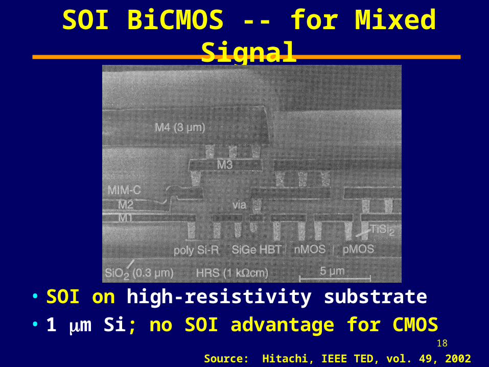
Source: Hitachi, IEEE TED, vol. 49, 2002
SOI BiCMOS -- for Mixed Signal
• SOI on high-resistivity substrate• 1 m Si; no SOI advantage for CMOS

19
Thin SOI
• Fully depleted collector SOI bipolar
EB C
buried oxide
substrate of SOI
n+n+ n
n+p+
0.1mn+
n+ subcollector
p+ p+n
EB Cn+
~ 2 m
Bipolar Transistors: from Bulk to Thin SOI
Bulk

20
EBC
n+
n+
p
n
A
A'A"n
depleted n collector region
A'"
A A' A"
Ec
EvE B
C
space-chargeregion
collectorreachthrough
A'"
buried oxide
substrate
• Electrons drift across depleted collector region towards reachthrough
Fully-Depleted-Collector SOI Bipolar
Source: J. Cai et al., 2002 Symp. VLSI Technology

21
SOI Vs. Bulk SiGe Bipolar Device
IBM’s ProductionSiGe Bipolar
Experiment SOI bipolar
C E B
Subcollector

22
Measured I-V Characteristics
0 1 2 3 40
4
8
12
16
20
IB0
=50pAIB step 1nA
I C (A
)
VCE
(V)
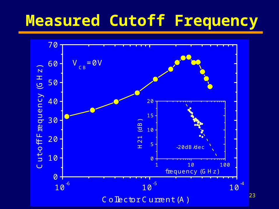
2310-6 10-5 10-40
10
20
30
40
50
60
70
1 10 1000
5
10
15
20
C
ut-o
ff F
requ
ency
(G
Hz)
Collector Current (A)
VCB
=0V
H2
1 (
dB
)
frequency (GHz)
-20dB/dec
Measured Cutoff Frequency
24
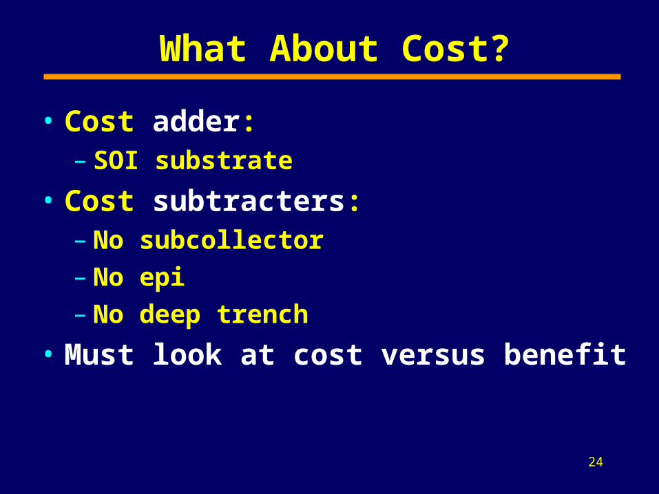
What About Cost?
• Cost adder:– SOI substrate
• Cost subtracters:– No subcollector– No epi– No deep trench
• Must look at cost versus benefit

25
Complementary BiCMOS
NPN PNP PMOS NMOS INDUCTOR
• No SOI • fT of npn = 25 GHz
• fT of pnp = 2.5 GHzSource: NEC, 1998 IEDM

26
EB
C
buried oxide
substrate of SOI
n+n+ n
n+n+ n+
EB
C
p+ p+p
p+ p+
pn+ n+ np+ p+
G
S D D
G
Sn+ p+
SOI Complementary BiCMOS
pnp npn nMOS pMOS
• npn, pnp, and CMOS on same thin SOI

27Source: Hitachi, IEEE TED, 1995
Advantage of Complementary Bipolar
28TimeT
ech
no
log
y P
erfo
rman
ce
CMOS
Summary
SOI BiCMOS
Mixed-Signal

29
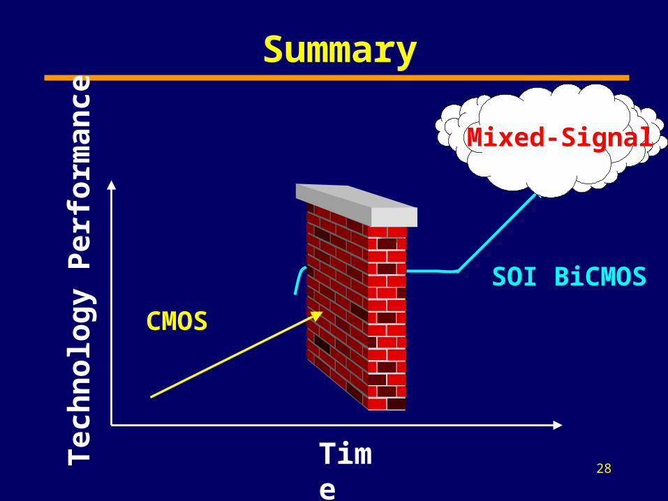
Summary
• Silicon technology evolution continues at rapid pace
• CMOS development is rapidly reaching its limits
• Opportunities around the corner of the redbrick wall
• SOI BiCMOS likely to emerge as preferred technology platform for mixed-signal applications