1 smart card physical interface - microchip...
TRANSCRIPT

APPLICATION NOTE
AVR1623: XMEGA Smart Card Reader
ATxmega128A1
Introduction
This application note describes how to use an Atmel® AVR® XMEGA® device to
connect to a smart card. The supplied code can easily be ported to support any
Atmel device (ATmega, tinyAVR®, XMEGA, UC3, SAM) containing a timer
capable of outputting a high frequency clock signal at an I/O pin, an U(S)ART,
and optionally a TWI/I2C module.
Features
ISO7816 comparable smart card reader
Optional standalone smart card reader functionality
TWI/I2C control interface
Hardware suggestions for both class C and class B smart cards (1.8V and
3.0V)
Out of the box support for externally clocked asynchronous smart cards
Note: Some of the UC3 and SAM devices also offer a hardware solution for an
ISO7816 interface, which does not rely on any external components for
achieving half duplex serial communication.
Atmel-42624A-XMEGA-Smart-Card-Reader_ApplicationNote_AVR1623_112015
AVR1623: XMEGA Smart Card Reader [APPLICATION NOTE] Atmel-42624A-XMEGA-Smart-Card-Reader_ApplicationNote_AVR1623_112015 2
2
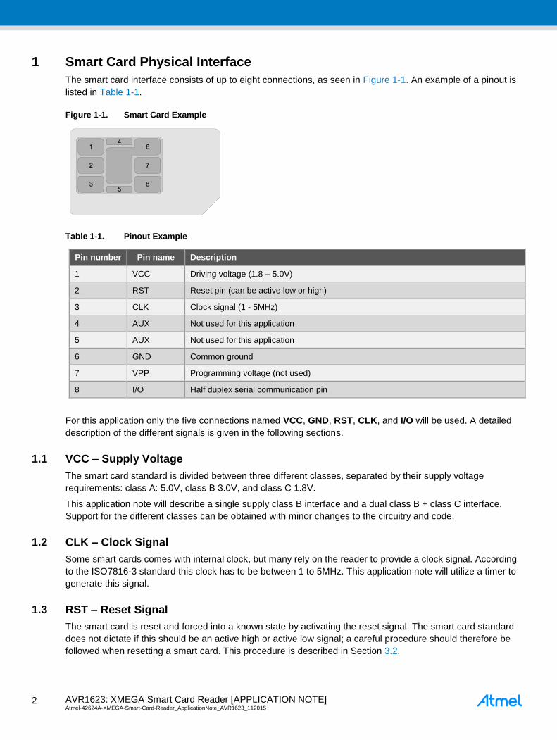
1 Smart Card Physical Interface
The smart card interface consists of up to eight connections, as seen in Figure 1-1. An example of a pinout is
listed in Table 1-1.
Figure 1-1. Smart Card Example
Table 1-1. Pinout Example
Pin number Pin name Description
1 VCC Driving voltage (1.8 – 5.0V)
2 RST Reset pin (can be active low or high)
3 CLK Clock signal (1 - 5MHz)
4 AUX Not used for this application
5 AUX Not used for this application
6 GND Common ground
7 VPP Programming voltage (not used)
8 I/O Half duplex serial communication pin
For this application only the five connections named VCC, GND, RST, CLK, and I/O will be used. A detailed
description of the different signals is given in the following sections.
1.1 VCC – Supply Voltage
The smart card standard is divided between three different classes, separated by their supply voltage
requirements: class A: 5.0V, class B 3.0V, and class C 1.8V.
This application note will describe a single supply class B interface and a dual class B + class C interface.
Support for the different classes can be obtained with minor changes to the circuitry and code.
1.2 CLK – Clock Signal
Some smart cards comes with internal clock, but many rely on the reader to provide a clock signal. According
to the ISO7816-3 standard this clock has to be between 1 to 5MHz. This application note will utilize a timer to
generate this signal.
1.3 RST – Reset Signal
The smart card is reset and forced into a known state by activating the reset signal. The smart card standard
does not dictate if this should be an active high or active low signal; a careful procedure should therefore be
followed when resetting a smart card. This procedure is described in Section 3.2.
AVR1623: XMEGA Smart Card Reader [APPLICATION NOTE] Atmel-42624A-XMEGA-Smart-Card-Reader_ApplicationNote_AVR1623_112015
3
3
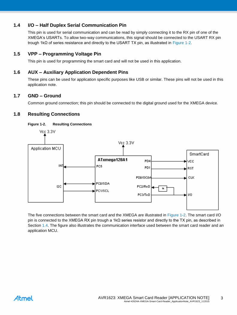
1.4 I/O – Half Duplex Serial Communication Pin
This pin is used for serial communication and can be read by simply connecting it to the RX pin of one of the
XMEGA’s USARTs. To allow two-way communications, this signal should be connected to the USART RX pin
trough 1kΩ of series resistance and directly to the USART TX pin, as illustrated in Figure 1-2.
1.5 VPP – Programming Voltage Pin
This pin is used for programming the smart card and will not be used in this application.
1.6 AUX – Auxiliary Application Dependent Pins
These pins can be used for application specific purposes like USB or similar. These pins will not be used in this
application note.
1.7 GND – Ground
Common ground connection; this pin should be connected to the digital ground used for the XMEGA device.
1.8 Resulting Connections
Figure 1-2. Resulting Connections
The five connections between the smart card and the XMEGA are illustrated in Figure 1-2. The smart card I/O
pin is connected to the XMEGA RX pin trough a 1kΩ series resistor and directly to the TX pin, as described in
Section 1.4. The figure also illustrates the communication interface used between the smart card reader and an
application MCU.

AVR1623: XMEGA Smart Card Reader [APPLICATION NOTE] Atmel-42624A-XMEGA-Smart-Card-Reader_ApplicationNote_AVR1623_112015 4
4
2 Power Considerations
As mentioned earlier, smart cards run on one of three possible supply voltages, depending on their class. For
this example the smart card VCC pin will be connected directly to an XMEGA GPIO pin. The ISO7816 standard
specifies that smart cards can draw up to as much as 100mA. This exceeds the limit for how much current can
be sourced by an XMEGA GPIO pin, but for demonstration purposes in this application the smart card is
powered directly from the GPIO pin on the XMEGA device. For an end application it is therefore recommended
using an external power supply to power the smart card.
Applying power to a smart card before it is properly seated in its socket could
result in voltage being applied to pins other than the smart card VCC pin, thereby
damaging the smart card. A controlled power supply should therefore be used to
ensure power is only supplied to the smart card when it is properly inserted into
the socket.
3 Interfacing a Smart Card
For this application note the smart card I/O pin and RST pin will be used to communicate with the smart card.
The I/O pin is a bidirectional interface, and is driven from both the smart card itself and the XMEGA. The reset
pin (RST) is controlled solely by the XMEGA and is used to ensure the smart card is in a known state before
communication is initiated.
3.1 Powering and Activating a Smart Card
Both active low and active high reset configurations are used for different smart cards. Because of this, special
care needs to be taken when powering a smart card. The ISO7816 standard dictates how this should be done.
The procedure should be as follows:
1. RST is pulled low.
2. The smart card is powered.
3. The interfacing device gets ready for incoming data.
4. A stable clock signal is provided to the smart card CLK pin.
5. Continue with the reset procedure, see Section 3.2.
3.2 Resetting the Smart Card
When resetting a smart card, the card should answer with an Answer-to-Reset (ATR) (see Section 3.3 for more
information about ATR).
A smart card is reset as follows:
1. Pull the RST line low.
2. If no ATR arrives within the next 40 000 cycles, it is assumed the smart card has an active high reset,
and the RST signal should be pulled high.
3. If an ATR still does not arrive within the preceding 40 000 cycles, it is assumed there is an issue with the
interface, and the reader, i.e. the XMEGA device, should deactivate the connection to the smart card and
the connections should be investigated.
AVR1623: XMEGA Smart Card Reader [APPLICATION NOTE] Atmel-42624A-XMEGA-Smart-Card-Reader_ApplicationNote_AVR1623_112015
5
5
3.3 Answer to Reset (ATR)
An ATR consists of a number of bytes describing the connected smart card. The exact content is specific to
different smart cards, and depends on their applications. For details on this, refer to your specific smart card
data sheet.
3.4 Character Frame
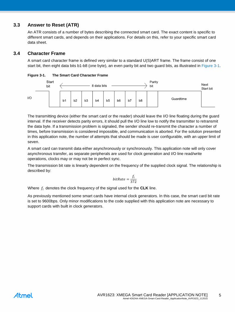
A smart card character frame is defined very similar to a standard U(S)ART frame. The frame consist of one
start bit, then eight data bits b1-b8 (one byte), an even parity bit and two guard bits, as illustrated in Figure 3-1.
Figure 3-1. The Smart Card Character Frame
The transmitting device (either the smart card or the reader) should leave the I/O line floating during the guard
interval. If the receiver detects parity errors, it should pull the I/O line low to notify the transmitter to retransmit
the data byte. If a transmission problem is signaled, the sender should re-transmit the character a number of
times, before transmission is considered impossible, and communication is aborted. For the solution presented
in this application note, the number of attempts that should be made is user configurable, with an upper limit of
seven.
A smart card can transmit data either asynchronously or synchronously. This application note will only cover
asynchronous transfer, as separate peripherals are used for clock generation and I/O line read/write
operations, clocks may or may not be in perfect sync.
The transmission bit rate is linearly dependent on the frequency of the supplied clock signal. The relationship is
described by:
𝑏𝑖𝑡𝑅𝑎𝑡𝑒 =𝑓𝑖
372
Where 𝑓𝑖 denotes the clock frequency of the signal used for the CLK line.
As previously mentioned some smart cards have internal clock generators. In this case, the smart card bit rate
is set to 9600bps. Only minor modifications to the code supplied with this application note are necessary to
support cards with built in clock generators.
AVR1623: XMEGA Smart Card Reader [APPLICATION NOTE] Atmel-42624A-XMEGA-Smart-Card-Reader_ApplicationNote_AVR1623_112015 6
6
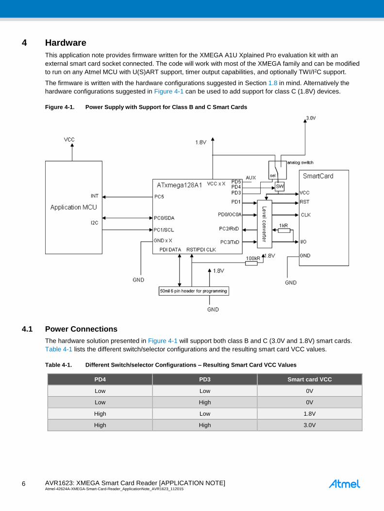
4 Hardware
This application note provides firmware written for the XMEGA A1U Xplained Pro evaluation kit with an
external smart card socket connected. The code will work with most of the XMEGA family and can be modified
to run on any Atmel MCU with U(S)ART support, timer output capabilities, and optionally TWI/I2C support.
The firmware is written with the hardware configurations suggested in Section 1.8 in mind. Alternatively the
hardware configurations suggested in Figure 4-1 can be used to add support for class C (1.8V) devices.
Figure 4-1. Power Supply with Support for Class B and C Smart Cards
4.1 Power Connections
The hardware solution presented in Figure 4-1 will support both class B and C (3.0V and 1.8V) smart cards.
Table 4-1 lists the different switch/selector configurations and the resulting smart card VCC values.
Table 4-1. Different Switch/selector Configurations – Resulting Smart Card VCC Values
PD4 PD3 Smart card VCC
Low Low 0V
Low High 0V
High Low 1.8V
High High 3.0V

AVR1623: XMEGA Smart Card Reader [APPLICATION NOTE] Atmel-42624A-XMEGA-Smart-Card-Reader_ApplicationNote_AVR1623_112015
7
7
5 Interfacing the Reader
The reader is configured with a TWI/I2C interface for communication with an interfacing application controller.
The communication protocol relies on various control words for configuring the reader itself and communication
with a connected smart card.
5.1 Addressing
As listed in Table 5-1, the TWI/I2C device address is set to be 0x21. Taking the R/W bit in the TWI address into
account gives the address 0x42 to write and 0x43 to read.
Table 5-1. TWI/I2C Device Address Set to 0x21
TWI/I2C base address TWI/I2C write address TWI/I2C read address
0x21 0x42 0x43
5.2 Configuration Registers
The reader has two configuration registers used for configuring the reader and the smart card interface. These
registers can be configured using the TWI/I2C interface with the command listed in Table 5-2.
Table 5-2. Command List
Description Address Command Data byte 1 Data byte 2
Write configuration 0x42 (0b10<<6)+SC_CFG0 SC_CFG1 CFG_CHECK

AVR1623: XMEGA Smart Card Reader [APPLICATION NOTE] Atmel-42624A-XMEGA-Smart-Card-Reader_ApplicationNote_AVR1623_112015 8
8
5.2.1 SC_CFG0 – Configuration Register 0
Bit 7 6 5 4 3 2 1 0
SC_CFG0 1 0 SHUTDOWN RETRY[2:0] VCARD[1:0]
Access W W W W W W W W
Reset 1 0 0 0 1 1 0 0
Bit [7:6]
These bits are part of the command and must always be ‘0b10’.
Bit 5 – SHUTDOWN
This bit activates or deactivates the connected smart card according to the process described in the
ISO7816 standard.
SHUTDOWN Action
0 Activate the smart card according to ISO7816 after updating the configuration registers
1 Shutdown the smart card
Bit [4:2] – RETRY
These bits define how many attempts should be made to retransmit a byte of data if NAK is received from
the smart card.
RETRY [4:2] Number of retries
000 0
001 1
010 2
… …
111 7
Bit [1:0] – VCARD
These bits configure the smart card reader pins according to the table listed in Section 4.1. With the cir-
cuitry proposed in Figure 4-1 or similar, these bits will define the voltage supplied to the connected smart
card PWR pin.
VCARD [1:0] Smart card voltage supply
00 0.0V(1)
01 1.8V(1)
10 3.0V(1)
11 Reserved for 5.0V operation Class A smart cards(2)
Notes: 1. Voltage change will not take effect unless an activation is run.
2. This application note does not suggest hardware for class A smart cards, but this can be achieved with minor
changes to the circuitry suggested in Figure 4-1.
AVR1623: XMEGA Smart Card Reader [APPLICATION NOTE] Atmel-42624A-XMEGA-Smart-Card-Reader_ApplicationNote_AVR1623_112015
9
9
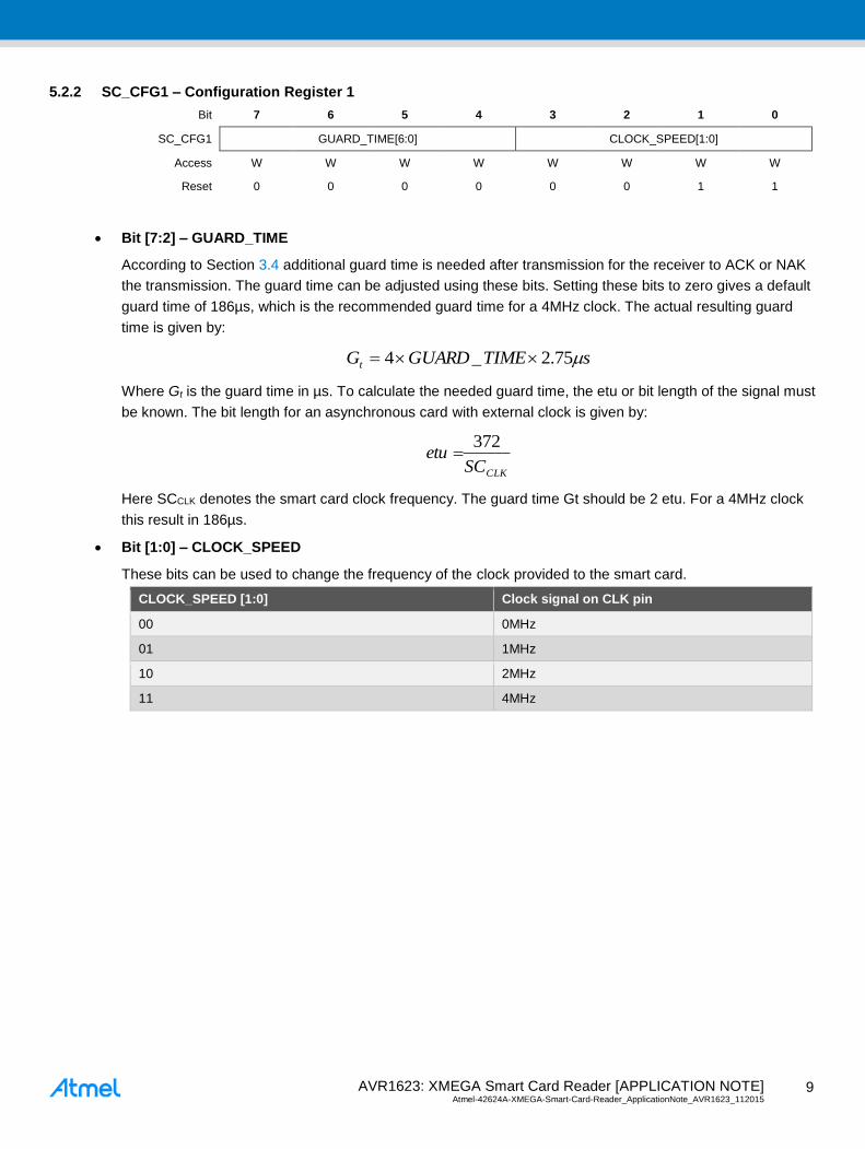
5.2.2 SC_CFG1 – Configuration Register 1
Bit 7 6 5 4 3 2 1 0
SC_CFG1 GUARD_TIME[6:0] CLOCK_SPEED[1:0]
Access W W W W W W W W
Reset 0 0 0 0 0 0 1 1
Bit [7:2] – GUARD_TIME
According to Section 3.4 additional guard time is needed after transmission for the receiver to ACK or NAK
the transmission. The guard time can be adjusted using these bits. Setting these bits to zero gives a default
guard time of 186µs, which is the recommended guard time for a 4MHz clock. The actual resulting guard
time is given by:
sTIMEGUARDGt 75.2_4
Where Gt is the guard time in µs. To calculate the needed guard time, the etu or bit length of the signal must
be known. The bit length for an asynchronous card with external clock is given by:
CLKSCetu
372
Here SCCLK denotes the smart card clock frequency. The guard time Gt should be 2 etu. For a 4MHz clock
this result in 186µs.
Bit [1:0] – CLOCK_SPEED
These bits can be used to change the frequency of the clock provided to the smart card.
CLOCK_SPEED [1:0] Clock signal on CLK pin
00 0MHz
01 1MHz
10 2MHz
11 4MHz

AVR1623: XMEGA Smart Card Reader [APPLICATION NOTE] Atmel-42624A-XMEGA-Smart-Card-Reader_ApplicationNote_AVR1623_112015 1
0
10
5.2.3 CFG_CHECK
Bit 7 6 5 4 3 2 1 0
SC_CFG1 CFG_CHECK[7:0]
Access W W W W W W W W
Reset 0 0 0 0 0 0 0 0
Bit [7:0] CFG_CHECK
This byte is used by the smart card reader to detect possible transmission errors in the received SC_CFG0
and SC_CFG1 packets sent to the reader over TWI/I2C. CFG_CHECK should equal a bitwise XOR between
SC_CFG0 and SC_CFG1. If a transmission error is detected, the smart card connection will be deactivated.

AVR1623: XMEGA Smart Card Reader [APPLICATION NOTE] Atmel-42624A-XMEGA-Smart-Card-Reader_ApplicationNote_AVR1623_112015
1
1
11
5.3 Interface Register
The interface register can be used to control the smart card reader GPIO pins, issue a reset signal to the smart
card, or placing the reader in sleep mode. The register is write-only, and all bits will be cleared after the written
command has been executed.
5.3.1 SC_INTERFACE
Bit 7 6 5 4 3 2 1 0
SC_INTERFACE 0 IODIS CKSTOP CARDRST AUX SLEEP CARDCK CARDIO
Access W W W W W W W W
Reset 0 0 0 0 0 1 0 0
Bit 7
This bit is a part of the command, and must always be written to ‘0b0’.
Bit 6 – IODIS
This bit selects one out of two possible operation modes for the smart card interface pins:
IODIS Action
0 The interface pins CLK, RST, and I/O will be driven as defined by the ISO7816 standard, and the
CARDCK, CARDIO, and CARDRST bits are ignored
1 The smart card interface pins CLK, RST, and I/O are driven as defined by the CARDCK, CARDIO,
and CARDRST bits
Bit 5 – CKSTOP
This bit can be used to stop the smart card clock. Some smart cards will enter sleep mode when the clock is
stopped.
CKSTOP Action
0 No action
1 The smart card clock is stopped(1)
Note: 1. If the smart card clock is stopped, the card must be reactivated according to the procedure described in
Section 3.1.
Bit 4 – CARDRST
The smart card reader response to setting this bit is dependent on the IODIS and the smart card reset mode
detected during the activation process. The reset pulse length is defined in firmware with a default duration
of 2ms.
CARDRST IODIS Action
0 0 No action
1 RST line driven low
1 0 The smart card interface pins CLK, RST, and I/O are driven as defined by the
CARDCK, CARDIO, and CARDRST bits
1 RST line driven high
AVR1623: XMEGA Smart Card Reader [APPLICATION NOTE] Atmel-42624A-XMEGA-Smart-Card-Reader_ApplicationNote_AVR1623_112015 1
2
12
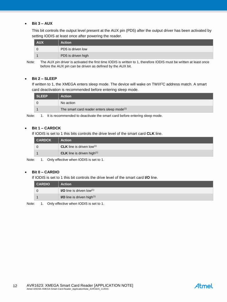
Bit 3 – AUX
This bit controls the output level present at the AUX pin (PD5) after the output driver has been activated by
setting IODIS at least once after powering the reader.
AUX Action
0 PD5 is driven low
1 PD5 is driven high
Note: The AUX pin driver is activated the first time IODIS is written to 1, therefore IODIS must be written at least once
before the AUX pin can be driven as defined by the AUX bit.
Bit 2 – SLEEP
If written to 1, the XMEGA enters sleep mode. The device will wake on TWI/I2C address match. A smart
card deactivation is recommended before entering sleep mode.
SLEEP Action
0 No action
1 The smart card reader enters sleep mode(1)
Note: 1. It is recommended to deactivate the smart card before entering sleep mode.
Bit 1 – CARDCK
If IODIS is set to 1 this bits controls the drive level of the smart card CLK line.
CARDCK Action
0 CLK line is driven low(1)
1 CLK line is driven high(1)
Note: 1. Only effective when IODIS is set to 1.
Bit 0 – CARDIO
If IODIS is set to 1 this bit controls the drive level of the smart card I/O line.
CARDIO Action
0 I/O line is driven low(1)
1 I/O line is driven high(1)
Note: 1. Only effective when IODIS is set to 1.
AVR1623: XMEGA Smart Card Reader [APPLICATION NOTE] Atmel-42624A-XMEGA-Smart-Card-Reader_ApplicationNote_AVR1623_112015
1
3
13
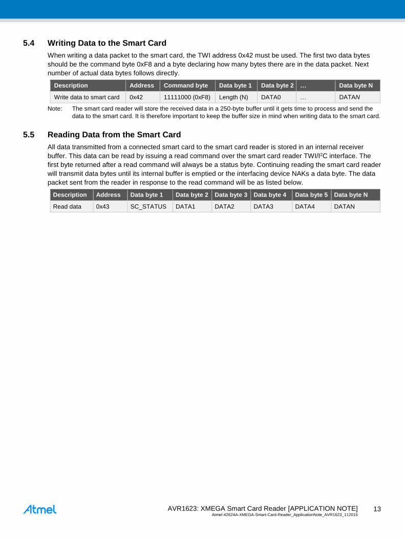
5.4 Writing Data to the Smart Card
When writing a data packet to the smart card, the TWI address 0x42 must be used. The first two data bytes
should be the command byte 0xF8 and a byte declaring how many bytes there are in the data packet. Next
number of actual data bytes follows directly.
Description Address Command byte Data byte 1 Data byte 2 … Data byte N
Write data to smart card 0x42 11111000 (0xF8) Length (N) DATA0 … DATAN
Note: The smart card reader will store the received data in a 250-byte buffer until it gets time to process and send the
data to the smart card. It is therefore important to keep the buffer size in mind when writing data to the smart card.
5.5 Reading Data from the Smart Card
All data transmitted from a connected smart card to the smart card reader is stored in an internal receiver
buffer. This data can be read by issuing a read command over the smart card reader TWI/I2C interface. The
first byte returned after a read command will always be a status byte. Continuing reading the smart card reader
will transmit data bytes until its internal buffer is emptied or the interfacing device NAKs a data byte. The data
packet sent from the reader in response to the read command will be as listed below.
Description Address Data byte 1 Data byte 2 Data byte 3 Data byte 4 Data byte 5 Data byte N
Read data 0x43 SC_STATUS DATA1 DATA2 DATA3 DATA4 DATAN
AVR1623: XMEGA Smart Card Reader [APPLICATION NOTE] Atmel-42624A-XMEGA-Smart-Card-Reader_ApplicationNote_AVR1623_112015 1
4
14
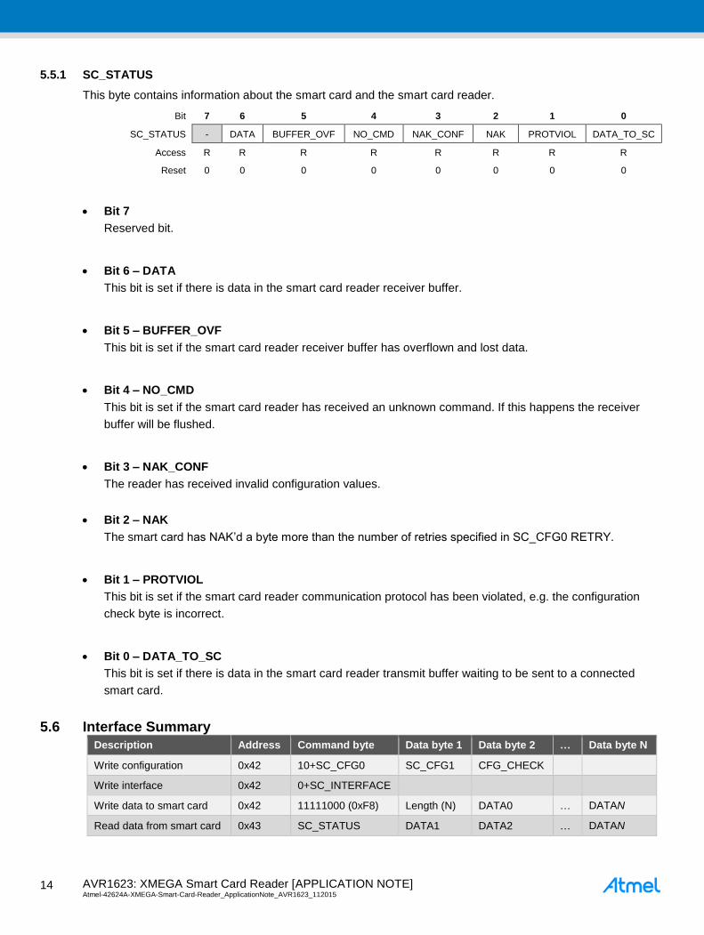
5.5.1 SC_STATUS
This byte contains information about the smart card and the smart card reader.
Bit 7 6 5 4 3 2 1 0
SC_STATUS - DATA BUFFER_OVF NO_CMD NAK_CONF NAK PROTVIOL DATA_TO_SC
Access R R R R R R R R
Reset 0 0 0 0 0 0 0 0
Bit 7
Reserved bit.
Bit 6 – DATA
This bit is set if there is data in the smart card reader receiver buffer.
Bit 5 – BUFFER_OVF
This bit is set if the smart card reader receiver buffer has overflown and lost data.
Bit 4 – NO_CMD
This bit is set if the smart card reader has received an unknown command. If this happens the receiver
buffer will be flushed.
Bit 3 – NAK_CONF
The reader has received invalid configuration values.
Bit 2 – NAK
The smart card has NAK’d a byte more than the number of retries specified in SC_CFG0 RETRY.
Bit 1 – PROTVIOL
This bit is set if the smart card reader communication protocol has been violated, e.g. the configuration
check byte is incorrect.
Bit 0 – DATA_TO_SC
This bit is set if there is data in the smart card reader transmit buffer waiting to be sent to a connected
smart card.
5.6 Interface Summary
Description Address Command byte Data byte 1 Data byte 2 … Data byte N
Write configuration 0x42 10+SC_CFG0 SC_CFG1 CFG_CHECK
Write interface 0x42 0+SC_INTERFACE
Write data to smart card 0x42 11111000 (0xF8) Length (N) DATA0 … DATAN
Read data from smart card 0x43 SC_STATUS DATA1 DATA2 … DATAN

AVR1623: XMEGA Smart Card Reader [APPLICATION NOTE] Atmel-42624A-XMEGA-Smart-Card-Reader_ApplicationNote_AVR1623_112015
1
5
15
6 Interrupt Pin
The smart card reader has an interrupt pin (PC5) used for signaling that the reader receiver buffer contains
data waiting to be sent to the application processor. Connecting this pin is optional, but if left unconnected the
smart card reader will be unable to signal when there is data in the receiver buffer, and the application
processor will have to poll for data to avoid buffer overflows.
The interrupt pin is low when the smart card reader receiver buffer is empty. If there is data in the receiver
buffer the interrupt pin is driven high until the buffer is emptied.
7 Sleep Mode
After power-on the smart card reader is put in the Power Down sleep mode to conserve energy. When the
reader is in sleep mode all unused peripherals are turned off and all unused ports are pulled up to give them a
defined state. Any address match on the TWI bus will bring the reader out of sleep and put it in idle mode,
where it is ready to access a connected smart card. The reader can be put back to sleep using the SLEEP bit
in the SC_INTERFACE register. It is recommended to deactivate any connected smart card before the reader
is put in sleep mode as the smart card clock is stopped when the reader goes to sleep.

AVR1623: XMEGA Smart Card Reader [APPLICATION NOTE] Atmel-42624A-XMEGA-Smart-Card-Reader_ApplicationNote_AVR1623_112015 1
6
16
8 Revision History
Doc Rev. Date Comments
42624A 11/2015 Initial document release.
AVR1623: XMEGA Smart Card Reader [APPLICATION NOTE] Atmel-42624A-XMEGA-Smart-Card-Reader_ApplicationNote_AVR1623_112015
1
7
17
Atmel Corporation 1600 Technology Drive, San Jose, CA 95110 USA T: (+1)(408) 441.0311 F: (+1)(408) 436.4200 www.atmel.com
© 2015 Atmel Corporation. / Rev.: Atmel-42624A-XMEGA-Smart-Card-Reader_ApplicationNote_AVR1623_112015. Atmel®, Atmel logo and combinations thereof, AVR®, Enabling Unlimited Possibilities®, tinyAVR, XMEGA®, and others are registered trademarks or trademarks of Atmel Corporation in U.S. and other countries. ARM®, ARM Connected® logo, and others are the registered trademarks or trademarks of ARM Ltd. Other terms and product names may be trademarks of others. DISCLAIMER: The information in this document is provided in connection with Atmel products. No license, express or implied, by estoppel or otherwise, to any intellectual property right is granted by this document or in connection with the sale of Atmel products. EXCEPT AS SET FORTH IN THE ATMEL TERMS AND CONDITIONS OF SALES LOCATED ON THE ATMEL WEBSITE, ATMEL ASSUMES NO LIABILITY WHATSOEVER AND DISCLAIMS ANY EXPRESS, IMPLIED OR STATUTORY WARRANTY RELATING TO ITS PRODUCTS
INCLUDING, BUT NOT LIMITED TO, THE IMPLIED WARRANTY OF MERCHANTABILITY, FITNESS FOR A PARTICULAR PURPOSE, OR NON-INFRINGEMENT. IN NO EVENT SHALL ATMEL BE LIABLE FOR ANY DIRECT, INDIRECT, CONSEQUENTIAL, PUNITIVE, SPECIAL OR INCIDENTAL DAMAGES (INCLUDING, WITHOUT LI MITATION, DAMAGES FOR LOSS AND PROFITS, BUSINESS INTERRUPTION, OR LOSS OF INFORMATION) ARISING OUT OF THE USE OR INABILITY TO USE THIS DOCUMENT, EVEN IF ATM EL
HAS BEEN ADVISED OF THE POSSIBILITY OF SUCH DAMAGES. Atmel makes no representations or warranties with respect to the accurac y or completeness of the contents of this document and reserves the right to make changes to specifications and products descriptions at any time without notice. Atmel does not make any commitment to update the information contained herein. Unless specifically provided otherwise, Atmel products are not suitable for, and shall not be used in, automotive applications. Atmel products are not intended,
authorized, or warranted for use as components in applications intended to support or sustain life.
SAFETY-CRITICAL, MILITARY, AND AUTOMOTIVE APPLICATIONS DISCLAIMER: Atmel products are not designed for and will not be used in connection with any applications wh ere the failure of such products would reasonably be expected to result in significant personal injury or death (“Safety -Critical Applications”) without an Atmel officer's specific written consent. Safety-Critical Applications include, without limitation, life support devices and systems, equipment or systems for the operation o f nuclear facilities and weapons systems. Atmel
products are not designed nor intended for use in military or aerospace applications or environments unless specifically designated by Atmel as military-grade. Atmel products are not
designed nor intended for use in automotive applications unless specifically designated by Atmel as automotive-grade.