1 sensor and simulation notes note 86 some further
TRANSCRIPT

-\.-,- 1
Sensor and Simulation NotesNote 86
28 June 1969
Some Further Considerations for the CircularParallel-Plate Dipole
Capt Carl E. BaumAir Force Weapons Laboratory
Abstract
A previous note contained calculations of various featuresof the circular parallel-plate dipole; this note continues thesecalculations. In this note various problems are considered, in-cluding the frequency response characteristics of a resistive rodused as the output resistor, the effect of the thickness of thesensor disk electrodes on the equivalent height, the effect ofdielectric spacers on sensor capacitance and equivalent height,the electric field distortion near the edge of a conductingground plane with a square edge, and the electric field distor-tion of a circular ground plane of nonzero thickness by consider-ing it as an oblate spheroid.
—. -.. -. ___,.,._— .— ...-—... . --——. .---. —— -— -- -.
I. Introduction
In a previous notel we have treated some of the design con-siderations for a circular parallel-plate dipole. These consid-erations included the capacitance and equivalent height of thesensor, the frequency response of the sensor associated with aresistor inserted between the plates and in series with a low im-pedance output cable, and the perturbation of the electric fieldproduced by a surrounding dielectric shell.
In this note we consider several more problems associatedwith this type of sensor. First we consider the response of auniform conducting dielectric rod as the output resistor. Thiscan be compared with the response of a conducting tube in theprevious note. Second we consider the error introduced into theequivalent height by the non zero thickness of the circular diskelectrodes. Third we consider the errors introduced into the ca-pacitance and equivalent height by the use of dielectric spacers.Finally we consider the error introduced into the incident fieldby the presence of a disk of finite thickness which might be usedas a ground plane, either between the two electrodes of a differ-ential sensor, or adjacent to a large conducting surface andforming one side of a single ended sensor.
II. Short Circuit Current for a Resistive Rod
In reference 1 we considered the output resistor as a cy-lindrical shell of radius Y. with surface resistance Rs. ForRs >> Z it was found that the total current flowing alOng thissheet has a flat response to the incident wave,up to frequenciessuch that the wavelength is of the order of Yfiwhere Z is thewave impedancegiven by2
z f&=E
.of the medium containing the i~cident wave. Z is
(1)
where u and E are the permeability and permittivity, respectively,of this medium; the conductivity of this medium was assumed to bezero. The medium inside the resistive shell was assumed to havethe same electromagnetic parameters as the external medium.
While the total current on this cylindrical shell has arather high frequency response there are still other problems to
1. Capt Carl E. Baum, Sensor and Simulation Note 80, The CircularParallel-Plate Dipole, March 1969.
2. Rationalized MKSA units are used throughout.
1
.
consider. The current on the resistor must be related to the cur-rent into some other device which records this current or trans-ports the current to some other position for eventual recording.The manner of connecting the resistor to some device such as acoaxial cable can significantly influence the high-frequency char-
.—.
acteristics of the current into the cable. For example, theremay be currents in the output cable associated with displacementcurrent between the sensor plates and in the.resistor structure.There are then problems to be considered concerning the geometryOf how the resistor current gets into the output circuitry.
In figure 1 we show a possible geometry for the output re-sistor, including the connection to some output circuitry. Forthese calculations the resistor is taken as a uniform rod oflength b, radius Ytivity a.
or permeability Pr permittivity el~and conduc-The propagation constant in the resistor is then
(2)
The propagation constant in the medium between the plates is
K= um (3)
Note that this resistor is placed between the plates in a mannersuch that there is a narrow annular sl~t (with width small com-pared to Yo) in the perfectly conducting sheet (the plane z = O)around the resistor. The signal to the coaxial cable or otheroutput circuitry passes through this narrow annular slot. Onepurpose of choosing this geometry is so that with this annularslot shorted out we can calculate the short circuit current atthe slot as a boundary value problem in cylindrical coordinates.Such a calculation includes the displacement current in the re-sistor. In reference 1 we considered a resistive tube; with thepresent type of output connection one would have to add the dis-placement current inside the tube to the conduction current alongthe wall of the tube in order to find the short circuit currentinto the type of output connection being presently considered.In this note we only consider the short circuit current from thepoint of view of determining optimum resistor dimensions and con-ductivities . We do not here consider the source impedance pre-sented to the output circuit.
Referring again to figure 1 note that the output circuitryoccupies a volume with finite extent in the z direction. In ref-erence 1 we considered the ideal case of two coaxial disks atz = &b. In a real sensor the signal has to come out somewhere.We assume for the present calculations that the signal is takenout near z = O on the z axis by including a conducting plate offinite thickness centered between the conducting disks. The
2

- —. y ispointingintothepage.
IEinc@ Hinc
Iz
RESISTOR
ANNULARSLOT
z=b
Figure 1. IDEALIZED RESISTOR WITH ANNULAR-SLOT OUTPUT
3

output circuitry would be inside this plate. Another case of in-terest is with a single disk at z = b and an infinite groundplane at z = O, in which case the output circuitry is below z = Oas in figure 1. A differential sensor_stith two symmetrical diskshas two resistors like the one shown in figure 1. We considerone resistor, the results applying equally well for two, as wouldbe used in a differential sensor.
In designing a parallel-plate dipole of this type there area few basic parameters normally established. These include thedisk position (z = b) which establishes the equivalent height ofthe dipole, the sensor capacitance, and the resistance of the re-sistor at the sensor output. With these parameters and whetherthe sensor is to be single ended or differential established onethen would like to maximize the frequency response of the sensor.In the present calculations we seek to make the short circuitcurrent from the resistor be uniform with frequency to the maxi-mum frequency possible for the case that the resistor is a uni-form circular rod. Considering a single resistor of length b asin figure 1 we have a resistance
b‘2 = ~y2a (4)
o
R2 and b are both considered as fixed numbers while Y. and IScanbe varied to optimize the short circuit current from the resistor.
Instead of Y~ we then define a characteristic distance whichis fixed by choic~ of R2
Then define a normalized
Let
Y. ‘1P=qf E =—
r E
frequency as
(5)
(6)
(7)
be dimensionless parameters. For fixed ~r we wish to find thebest value of p which optimizes the frequency response of theshort circuit current as expressed in terms of a.
4
Some parameters of interest can now be written as
KYO = ap —
K. 1/2
‘lyo.ap+ “~1’ ‘apq= ap[Er - 1
where we have defined
The
and
‘l=[cr-iq==
wave impedance in
‘“m
[ 1&ll’2 = ‘r - L 1’2lTap2
(8)
(9)
the resistor is
(lo)
we have the convenient relations
‘1 K 1—= —= —z ‘1 q
‘1—= -i(a + iucl)‘1
‘lKl = Lull
betw=en thepropagatingin the form
(11)
With the above preliminaries taken care of we go to theboundary value problem. As in reference 1 we assume an incidentplane waveand z = b)components
two perfectly conducting surfaces (Z = Oin the *X direction with only two field(with el~t suppressed)
Ez= ~ ~-iKYcos (@)
= Eoe-lKx oinc
(12)
E. EH =-~e-lKx=-#e
-iKYcos (@)
Y“lnc
5

where we have a cylindrical coordinateto cartesian coordinates (x, Y, Z) as
x=’+’ Cos(f.$), Y = Y sin($)
system (Y1 $r Z) related
—.— (13)
In cylindrical coordinates the incident wave has the expansions
[
m
Ez = E. Jo(KY) + 2X (-i)nJn(K’+)~Os(n@)inc n=1 1
E. m Jn(KY)
‘Y. ‘-iz--2~(-i)n KY sin(n$)
mc n=1
(14)
E.
[
m
%. ‘-i~J:(KY) + 2X (-i)nJ;(Ky) cos(n$)
mc n=1
Primes on the Bessel functions denote the derivative with respectto the argument. Two components of the wave inside the resistor(Y < Yo) are
[
C.u
E = E. aoJo(KIY) + 2~ (-i)nanJn(Kly) cos(n$)‘1 n=1 1‘$1= ‘1
The reflectedby
E
[# aoJ~(KIY) + 25 (-i)nanJ~(Kl’f’)cos (n@)1 n=1 1
wave (for Y > Yo) has two Of its components
(15)
given
[
al
(L) (KY} cos(n$)= E b H(2) (KY) + 2~(-i)nbnEinE‘2 ’00 n=1 1
(16)
{2) ~Ky)Cos(m$)E
[‘2){KY) + 25 (-i)nbnHn~$2 = -i : boHo
n=1 !
This reflected wave is taken as a purely outward propagating waveas was also done for the example in reference 1. Thus the size
6

of the conducting plates is assumed infinite making this a high-frequency or early-time calculation.
To find the coefficients in the field _expansions first makeEz continuous at Y = Y. giving
—..
(17)‘2)(KYO)anJn(KIYo) = Jn(KYo) + bnHn
Making Ho continuous at Y = Y. gives
(KIYo) = *[J: (KYO) + bnH:2) tKYo)] (18)
rewritten aswhich can be
J;(KYo) + bnH:2)iKYo) (19)(KIYO) = qanJ:(KIYo)
Solving for an we have
J (KlYo)H;2) iKyo)]n‘2)(KYO) -an[qJ~(Klyo) ‘n
= J;(Kyo)H~2) (KYO) J (KYO)H:2)\KYo)n
(20)2i= 1TK%
have used a Wronskian
short circuit current
relation for the Bessel
across the annular slot
functions.
at Y = YoThegiven
I =
byis
E; aoJ:(Kp’o)
1-J2?T
‘$ y=y
Yod@c o
i27rYo
4E‘2)tKYo)]
-1=- + J: (KIYo)[qJ: (KlYo)Hj2) (Kyo) - JO(KIYO)HO
1A
(21)
7

If we expand the Bessel functions for small arguments (small inmagnitude) we find for small IKYOI and lKIYo\ the asymptotic re-lation
—.
(22)
This, of course, is the sum of the low-frequency conduction anddisplacement currents in the resistor. Note that this asymptoticform in equation 22 is not the asymptotic form for low frequencyu but for small IKYOI and \KIYo~ so that the leading term of theBessel function expansions is used. If an asymptotic form forsmall u is used other terms related to the resistor size (whichmight be thought of as an inductive effect) also enter in. Anappropriate normalizing current is then
(23)
so that in normalized form we have
I4J:(K1YO)
[qJ:(Kl~o)Ho‘2)(KYO) - (2)[KY ~;l—=10 JO(KIYO)HO (24)
@ZIKo
In terms of the normalized parameters a, p, and q defined pre-viously we have
(25)
so that we have
I ‘2)(Up)~ J’(apq)[qJ:(apq)Ho—=10 a O
- Jo(apq)H:2) {ap)]-l (26)
In figures 2 and 3 the magnitude and phase of I/I. areplotted as functions of the normalized frequency a for ~r = I andGr = 10 and for several values of the parameter p. Note in fig-ure 2 for &r = 1 that based on the magnitude of 1/10 the bestfrequency r~sponse curve has p s 0.4.- In figure 2 for &r = 10the best case is with p ‘ 0.15. For thesethe frequency response is roughly constantized frequency which is roughly a ‘ 7.
cases the magnitude ofto the highest normal-
8

10’ I I I [ I I I I 1 I I I I I I I I I I I I I I
i
J_
10
I0°
16’2
.01
I I I I I I I I 1 I i I I I I I I I I I I I I
X162 Id 10° 10’ 2xa
A. Magnitude
10’
2 i I I
p’2
1,5
0 ‘.1
-i 1 1 I I I I I I I I I I I I I ! I I I 1 I I I2X152 15’ 10° 10’ 2x
a
B. Phase
10’
Figure 2. SHORT CIRCUIT CURRENT : ~r ‘ 1
\ 9

10[
J_10
10°
2
()arg L10
0
I I I I I I I
1 I I I I 1i16’2x162 10’ 2XI0’
a
A. Magnitude
I I I I I I I I I I I I III 1 1 I i I III r
)
I I I I I I 1 I I I I I I I I I I f I I I I I I 1I I
2X152 16’ 10° 101 2XI0’a
Figure 3. SHORT CIRCUIT CURRENT :$. ~ iO
10

For a particular value of p the resistor radius and conduc-tivity can be found from
and
0 b= ‘2=nY:R2 22ITpbZ
(27)
(28)
Note that as R2 is increased the optimum Y. is decreased and thecorresponding u for maximum frequency response is increased.
As a rough physical interpretation there are at least twoeffects which make the frequency response nonflat at high fre-quencies. There is the displacement current as shown in equation22. The displacement current tends to increase the current mag-nitude at high frequencies. For fixed R2 the effect of the dis-placement current is decreased by increasing o and correspondinglydecreasing Yo. The second effect is that as the frequency is in-creased and wavelengths in the resistor become of the order of Y.(in magnitude) the current is not uniform in the resistor andskin depth limitations enter the problem. This decreases themagnitude of the net current flowing through the resistor. Theoptimum value of p, and thus the optimum value of Y. for fixedb and R2, is chosen to roughly compensate these two effects tomaximize the frequency response.
The Bessel functions of real and complex arguments were cal-culated using a computer code discussed in a previous note.3
III. Error Introduced into the Equivalent Height by Non ZeroThickness of the Disk Electrodes
One of the fundamental parameters of the circular parallel-plate dipole is its equivalent height. In this section we con-sider the effect of finite thickness of the one or two circulardisk electrodes on the equivalent height. This problem is con-sidered from a quasi static or low frequency viewpoint.
3. Richard C. Lindber~, Mathematics Note 1, BESSEL: A Subroutinefor the Generation of =essel Functions with Real or Complex Argu-ments, October 1966.
11

In figure 4 we show a cross section view of a circular par-allel-plate dipole with spacing 2b between the disks (insidefaces) and with each disk of thickness w; the disk radius+is a.In another note we have shown that th~.equivalen$ height heq isthe same as the mean charge separation distance ha. Since thetwo thick disks are both symmetric about the z axis we have onlya z component of the equivalent height and can write
K =h:=~a=ha:zeq eq z(29)
where ~z is a unit vector in the z direction and we have defined
(30)
To calculate the equivalent height we calculate the mean chargeseparation distance using the quasi static or low-frequency chargedistribution on the antenna with no incident field and with a pos-itive charge Q on the upper electrode (z = b to z = b + w) andwith -Q on the lower electrode.
Let the upper electrode have voltage +V and the lower elec-trode -V. The
c .QZ!v
Using symmetryculated from
capacitance of the sensor is
(31)
about the z = O plane the equivalent height is cal-
(32)
where V+ is the volume of the upper electrode and p is the chargedensity. Our objective is to find approximate lower and upperbounds for heq which we call hl and h2 respectively so that
h <h < h2l–eq–
(33)
4. Capt Carl E. Baum, Sensor and Simulation Note 69, Design of aPulse-Radiating Dipole Antenna as Related to High-Frequency andLow-Frequency Limits, January 1969.

y ispointinginto the page.
z:b+w
~:a V:a
z:bz
Figure 4. TWO EQUAL THICK COAXIAL CIRCULAR DISKS
13

Of course we would like h2 - hl to be as small as possible tominimize the error in designing such a sensor for a particular‘eq ●
Clearly a lower bound for heq is ~ust
hl = 2b
since all the charqe is located at Izl > b.
(34)
We could also use2(b + w) for an up~er limit on he but tisingthe capacitanceformulas in reference 1 we can ge? a significantly tighter ap-proximate upper bound. First note that the surface charge den-sity on the inner face (z = b) of the upper electrode has a lowerbound as
(35)
where E is the permittivity. This is because -V/b is the averagevertical electric field (average over z) between the electrodes(lz~ : b, IYl : a) and the maximum field magnitude for each Y oc-curs on the electrodes. The field enhancement is particularlystrong near the edge of the electrodes (’.? = a) . Let Q1 be thetotal charge on the inner face (z = b) of the upper electrode. Alower bound for Q1 is then
(36)
This simply says that the charge on the inside of the disk islarger than the charge if &he field were uniform because of thefringing fields. Another way to look at this is to look at theelectric field lines which terminate on charges on the insidesurfaces of the two disks (z = tb) . These field lines bulge out-wards, some extending be ond Y = a;
7the average cross section
area (at fixed z with [z < b) through which these field linespass is greater than na2. This makes the capacitance associatedwith the inside surfaces greater than c~a2/(2b) .
Let Q2 be defined by
(37)
From equations 31 and 36 we have the inequality
14

Q2<Q-+T~2= 2VC - E ; na2
Now to obtain an upper bound for--heqwe
heq < :[Q1b + Q2(b + w)]
This is greater than heq because Q2z between b and b + w. The averageless than b + w.
From equation 36 we can define
(38)
have
(39)
is distributed over values ofz associated with Q2 is then
(40)
For Q1 and Q2 we then have
vQ1=sFna2+Q3
(41)
Q2 ‘Q-E~Ta2-Q3
The inequality in equation 39 can then be written as
h ~{[E ~ ~a2veq ‘Q +Q3]b+[Q-s~na2 -Q3](b+w)} (42)
or
heq < ~{Qb + [Q - c ~ ~a2 - Q31w}
[
Q3
1=2b+21-~~a2-—w
Q
[
2 Q3
1=2b+ 2 1 - ~- —wQ
Since Q3 is positiveing the inequality.
(43)
we can drop this term while still maintain-Thus for our upper bound we take
15

‘2 [=2b+2w l-$
Note for large a/b that
[1
‘2-hl=2w1-@
c~a2
2b 1Capproaches ‘s~~2\(2b).
z~a2
2b 1
(44)
We now have
(45)
and for large a/b this is much less than 2w. A convenient way towrite the bounds on heq is as
B can be considered a relative error bound
(46)
in calculating heq.
To get an estimate for B and h2 we can use an approximatecapacitance formula discussed in reference 1. This is theKirchoff approximation which includes the non zero disk thickness.This approximation is
Then we have
For small w/b and for large a/b this is roughly
B’ #[in(+) - 11
(48)
(49)
Iv. Error Introduced into the Capacitance and Equivalent Heightby Dielectric Spacers
Assume that dielectric spacers are used to hold the twodisks or disk plus large ground plane at a fixed separation, i.e.the spacers establish b. Let these spacers have a dielectricconstant c~ and let them have shapes which are independent of zbetween the plates (~z~ < b, [VI < a). Let the total cross
16
section area of these spacers at each fixed z (with IzI < b)equal As. The electric field between the plates is approximatelya uniform Ez for large a\b if positions near the disk edges arenot considered. The increase in.capacitance due to these spacersis then
ACs ‘ (ss - &) &
The relative increase in the capacitance is defined by
(50)
(51)
If we approximate C by s~a2/(2b) for lar9e a/b then ‘his ‘rat-ional increase is roughly
The use of dielectricheight of the sensor. Thediscussed in reference 4, is fundame~tall~ the dipole moment ofthe sensor divided by the amount of charge transferred betweenthe sensor terminals. This charge is significant here because ascharge is transferred from’one disk to the other there is a polar-ization current in the opposite direction in the dielectricspacers. The dipole moment has only a z component given by
(52)
spacers also affects the equivalentmean charae separation distance~ as
Pz = 2b(Q - QJ
where the charge transferred between the electrodes is
Q = 2V(C + Cs)
(53)
(54)
and the charge
Qs = 2VCS
Note for thesezero thicknessthen
associated with the dielectric polarization is
(55)
calculations the two disks are assumed to haveand to be at potentials k37. The dipole moment is
17
Pz = 4bVC
and the equivalent height is
h ~zeg =ha=—=2bC:C
Q s
. Zbb’X’= 2b[l + f~]-l
For small f~ we have
heq = 2b[l - fs]
—.
(56)
—
(57)
(58)
The decrease in the equivalent height is then about 2bfs and f~is the approximate fractional decrease of the equivalent height.
The decrease in the equivalent height is then attributableto the dipole moment induced in the dielectric spacers which sub-tracts from the dipole moment due to the charge transferred be-tween the disks. The z component of the dipole moment in the di-electric is -justthe dielectric volume 2bA~ times the z componentof the polarization vector (Es - S)EZ in the dielectric or(SS - s)2bA~Ez; this is just -2bQs.
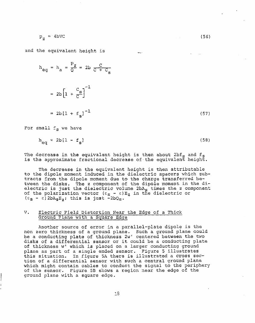
v. Electric Field Distortion Near the Edge of a ThickGround Plane with a Sauare Edae
Another source of error in a parallel-plate dipole is thenon zero thickness of a ground plane. Such a ground plane couldbe a conducting plate of thickness 2w’ centered between the twodisks of a differential sensor or it could be a conducting plateof thickness w’ which is placed on a larger conducting groundplane as part of a single ended sensor. Figure 5 illustratesthis situation. In figure 5A there is illustrated a cross sec-tion of a differential sensor with such a central ground planewhich might contain cables to conduct the signal to the peripheryof the sensor. Figure 5B shows a region near the edge of theground plane with a square edge.
,
18
.
I2a
II I
t—. b
b
w
A. Ground plane with circular disks
[
Einc
z: -W1
B. Edge of ground plane with coordinates os a two-dimensional problem
Figure 5, GROUND PLANE WITH SQUARE EDGE
19

In this section we consider the distortion of the incidentelectric field near the edge of such a ground plane at low fre-quencies so that we can use a quasi static approach. The groundplane is considered as a circular disk_gf non zero thickness 2w’and radius a’ with a’ >> w’. Near the edge of this disk we ap-proximate the geometry as two dimensional by neglecting the curv-ature of the edge. AS shown in figure 5B we set up a coordinatesystem based on the edge. Only two coordinates x’, z are of in-terest with x’ = O on the edge and z = O centered halfway’in thedisk; z = w’ is the top surface of the disk. The boundary con-ditions are that the electric potential be a constant (which wetake to be zero) on the disk surface and on the positive x’ axis.We are of course considering the case where the static incidentelectric field is uniform and can be written as
2. = Eo:zlnc (59)
We only consider the region z > 0 for x > 0 and z > w’ for x < 0.The sensor electrodes are assufiedabsent–for these–calculations.
Define a complex variable as
x : x’ + jz (60)
An appropriate conformal transformation for this geometry is5
1/2x = ‘;[(*2 - 1) + arccosh(v)] (61)
where ~ is another complex variable which we write as
$ = u+ jv (62)
The electric potential function is a constant times v since forlarge 1~1 we have the asymptotic relation
x =W+t) + O(ln($))
The electric potential function is then -w’Eov/n.
(63)
5. R. V. Churchill, Complex Variables and Applications, 2nd ed. ,McGraw Hill, 1960, p. 291.
20

Along the top surface of the disk (z = w“’,X’ < 0) we have
[
1/2w’ 2
x’ =p-(u - 1) 1+arccosh(-u)— .– (64)
while v = O and u < -1. The electric field just above this sur-face has only a z component and can be calculated as
w’E
()
-1
[
-1/2 1-1/2 -10 ax’
Ez=-~F =-EO-(U2 -1) u- (U2 - 1)
-1 1/2[1
=E”Ou+l
Now for u << -1 so that x’ << -w’ we have
x’ =
giving
(65)
(66)
1/2
= Eo[l - ‘~1 (67)
The relative field enhancement due to the ground plane thicknessis about Wl/(ITlXll). This gives one some idea about the distor-tion included in the field at the sensor electrodes at some dis-tance lx’I from the edqe of the qround plane. Define this rela-,,tive field enhancement- (for x’ <-0)(but still small compared to a’) is
w’%=-== h
as El which for lX1l >> w’approximately given by
(68)
VI. Electric Field Distortion for a Thick Ground PlaneApproximated as an Oblate Spheroid
We turn now from the field distortion near the edge of theground plane to the overall effect of the ground plane thicknesson the sensor accuracy. Consider the static electric field dis-tribution around the ground plane without the presence of the
21

disk electrodes. The ground plane of radius a’ and thickness 2w’excludes the electric field from its volume and thereby enhancesthe electric field at some positions in the vicinity of theground plane. Referring to figure 5A the sensor disk electrodesare each spaced from the nearest surface of the ground plane bythe distance b. The field enhancement due to the ground planethen increases the equivalent height to something greater than 2b(in the differential case). Thus we consider the enhancement ofthe incident electric field by the ground plane as an estimate ofthe error introduced into the calculation of the equivalent height(i.e. 2b). For this calculation we approximate the conductingground plane as an oblate spheroid.
In figure 6 oblate spheroidal coordinates are illustratedfor some cross section on a plane containing the z and x axes.This set of coordinates, for which we use g, L, $, is defined by6
x z r. cosh(~) sin(c) COS($) = Y COS($)
y s r. cosh(~) sin(3) sin($) = Y sin(o) (69)
z ~ r. sinh(~) cos(g)
where ‘Y,$, z is our cylindrical coordinate system as before andr. is just a convenient constant with dimension meters. We alsohave
Y = r. cosh(c) sin(L) (70)
The scale factors for this orthogonal curvilinear coordinate sys-tem are
1/2
‘c= hc = ro[cosh2(E) - sin2(C)]
(71)
ho = r. cosh(~) sin(?.)= Y
The general solution of the Laplace equation
6. Moon and Spencer, Field Theory fo~ Engineers, D. Van Nostrand,1961, chapter 10.
22

,
.
—
IEinc
Az //
//
v/‘$74’
////
bx
y is pointing into the page.
Figure 6, GROUND PLANE APPROXIMATED AS AN OBLATE SPHEROID :CROSS SECTION VIEW
23

v2@ = o
is of the form
(72)
.
.
where two terms in braces implies that some linear combination isused. Note that in general n and m need not be integers, but inthe present case they will be integers. P and Q are Legendrefunctions of the first and second kind respectively and we followthe definitions for general complex arguments and for the cut inthe complex plane (real axis between -1 and 1) as defined in astandard reference work.7 The problem discussed here is alsofound in reference 6.
Assume an incident potential of the form
0, = -Eoz = -Eoro sinh(~) cos(~)lnc (74)
The Legendre functions of interest are
= sinh(~) arccot[sinh(~)] - 1
= sinh(~) arctan[sin~(~)] - 1
The incident potential is then
oinc = Eoroip~(i sinh(C))p~(cos (c)) (76)
7. Abramowitz and Stegun, ed. , Handbook of Mathematics Functions,AMS 55, National Bureau of Standards, 1964, chapter 8.
24
‘
*
Referring to figure 6 note thatoblate ellipsoids of the form
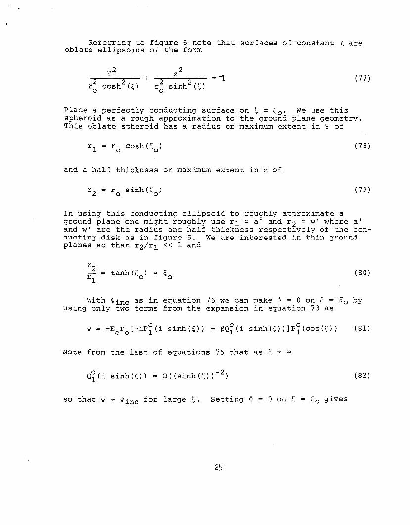
Place a perfectly conducting surfacespheroid as a rough approximation toThis oblate spheroid has a radius or
surfaces of-constant ? are
(77)
on C = tn. We use thisthe groufidplane geometry.maximum extent in Y of
‘1 = ‘o cosh(~o)
and a half thickness or maximum extent in z of
‘2 = ‘osinh(~o)
In using this conducting ellipsoid to roughly approximate aground plane one might rouahlv use rl ~ a’ and r. ‘ w’ whereand w’ are the radius andducting disk as in figureplanes so that r2\r1 << 1
fial~ thick~ess respect~vely of the
(78)
(79)
a’con-
5. We are interested in thin groundand
(80)
With @inc as in equation 76 we can make @ = O on ~ = go byusing only two terms from the expansion in equation 73 as
Q = -Eoro[-iP~(i sinh(g)) + 6Q~(i sinh(g) )lp~(cos(~)) (81)
Note from the last of equations 75 that as ~ + m
Q~(i sinh(g)) = O((sinh(~) )-2) (82)
so that @ + @inc for large ~. Setting @ = O on 5 = E. gives
25

.
,
The
@ =
=
Thehas
—
sinh(~o)
sinh(~o) arccot[sinh(co)l - 1(83)
potential is then
{
sinh(co) [sinh(~)arccot [sinh(C)] - 1]-Eoro s.inh(~)-
sinh(go)/COS(L)
arccot[sinh(co)] - 1
{
sinh(go)-Eoz 1 - sinh(Z)arccot[sinh(E)l - 1
sinh(~) sinh(&o)arccot[sinh(Eo) ] - 1I
The electric field has two components and is given by
(84)
(85)
maximum electric field magnitude occurs on E = Go where itonly a ~ component given by
EOCOS(L)
‘E <=< = 1/2{cosh(~o)
o [cosh2(~o)-sin2(<)1
sinh($o)[cosh(~o)arccot[sinh(Co)1
sinh(~o)arccot[sinh(co) ] - 1

e
Eocosh(?o)cos (G) l-tanh’(~o)=
1/2 l-sinh(:o)arccot[sinh(~o)l[cosh2(E-)-sin2 (C)]
= E.
.
1-1/2 n
sinhz (co) ‘ l-tanh’ (co)1+ cosh(~o)l
COS2(G)-sinh(go) arccot[sinh(Go) 1
E.
r= cosh(~o) 1 +
a
1-1/2
sinh2 (go){1-sinh(~
COS2 (g)o
arccot[sinh(go) 1}-1
(86)
This has its maximum value at ? = O (the z axis) where we have
E.E = {1max
- sinh(50)arccot[sinh(Co) 1}-1cosh2(&o)
For small Go we have
Ernax=
E. -1{1 - sinh(co) [~ - sinh(~o) + 0(5~)1}
cosh2(&o)
{
-1sinh(Co)
=Eo 1 - : + o(g)cosh2(Eo) /
-1
= Eo{l - ; E. + O(g:)}
Emax
= Eo{l + ;“-go} + 0(5:)
(87)
(88)
(89)

Call the relative increase in the maximum field 57; this is thenfor small go roughly
——
From this one can estimate how thin the ground planefor a given radius in order ta hold the sensor errorsired small number by using the rough approximationsa’ = rl.
VII. Summarv
(90)
should beto some de-VJ1~ r2 and
In this note we have found some optimum conditions for thedesign of a resistive dielectric rod to maximize the frequencyresponse of the short circuit current from the rod used as anoutput resistor.
Most of the note deals with various effects which detractfrom the sensor accuracy. In some cases error bounds are foundand in others approximations “to the relative error are found.These effects include thickness of the sensor electrodes andground plane and use of dielectric spacers. All these error cal-culations are based on solutions of the Laplace equation and thusonly apply for frequencies such that wavelengths are significantlylarger than sensor dimensions.
There are of course num~rous sources for small errors toenter the basic parameters of a circular parallel-plate dipoleand other types of electromagnetic sensors as well. Perhaps somefuture notes can further treat such error problems.
We would like to thank A2C Richard T. Clark and Mr. Larry D.Giorgi for the numerical calculations and graphs.
28