1 radiation damage effects in monolithic active pixel sensors implemented in an 0.18µm cmos process...
TRANSCRIPT

1
Radiation damage effects in Monolithic Active Pixel Sensors Implemented in an 0.18µm CMOS process
Dennis Doering, Goethe-University Frankfurt am Main
on behalf of the CBM-MVD-Collaboration
Outline- MAPS sensors- Mechanism of ionizing radiation damage- Going to a smaller 0.18µm feature size- Status of radiation hardness- Conclusion
ADvanced
MOnolithic
Sensors for

/17Dennis Doering: MAPS in 0.18µm CMOS process DPG Dresden March 2013 2/14
Applications of MAPS
Picture STAR
Picture CBM
International Linear ColliderCBM-Experiment (FAIR, GSI)
STAR-Experiment
MAPS are developed for applications as vertex detector since 1999 at IPHC (Strasbourg).
Possible ITS-Upgrade ALICE

/17/14
Operation principle of MAPS
Dennis Doering: MAPS in 0.18µm CMOS process DPG Dresden March 2013 3
+3.3VOutput
SiO2
N+ P+
P-P+
Diode
Epitaxial Layer
P-Well
Source Follower

/17/14
Noise measurement
Dennis Doering: MAPS in 0.18µm CMOS process DPG Dresden March 2013 4
1) Measured noise [mV] at the output 2) Charge-to-voltage conversion by the readout chain gain3) Calculate ENC [e]
+3.3V
Readout chain Gain
Measured noise [mV]
ENC [e]
Output

/17/14Dennis Doering: MAPS in 0.18µm CMOS process DPG Dresden March 2013 5
Classes of radiation damage
To be investigated and improved: Radiation hardness against…
… ionizing radiation:• Energy deposited into the electron cloud• Can ionize atoms and destroy molecules• Caused by charged particles and photons
… non-ionizing radiation:• Energy deposited into the crystal lattice• Atoms are displaced• Caused by heavy (fast leptons, hadrons),
charged and neutral particlesFarnan I, HM Cho, WJ Weber, 2007. "Quantification of Actinide α-Radiation Damage in Minerals and Ceramics." Nature 445(7124):190-193.
DPG Mainz 2012 HK 12.8
~10 14 neq with high-resistivity sensor
Discussed in this talk

/17/14
Ionizing radiation damage effects
Dennis Doering: MAPS in 0.18µm CMOS process DPG Dresden March 2013 6
1) Ionizing radiation damage generates electrons at Si/SiO2 interface2) Leakage current and ENC [e] increases3) Gain is constant4) Measured noise [mV] increases
+3.3V
Gain
Measured noise [mV]
ENC [e]
Output
0,0 0,2 0,4 0,6 0,8 1,00,00
0,05
0,10
0,15
0,20
0,25
0,30
Ga
in [
mV
/e]
Ionizing radiation dose [Mrad]
Gain [mV/e] Measured noise [mV] ENC [e]
M.Deveaux PHD-Thesis 2007 Su1-Mi15 +10°C 0.7ms
lines to guide the eye
0
1
2
3
4
5
Me
asu
red
no
ise
[m
V]
0
5
10
15
20
25
30
35
40
45
EN
C [
e]

/17/14
Going to smaller feature size
Dennis Doering: MAPS in 0.18µm CMOS process DPG Dresden March 2013 7
1) Measured noise [mV] decreases!
Mind the different scale!
0 10,00
0,05
0,10
0,15
0,20
0,25
0,30
Gain
[m
V/e
]
Ionizing radiation dose [Mrad]
Gain [mV/e] Measured noise [mV] ENC [e]
M.Deveaux PHD-Thesis 2007 Su1-Mi15 +10°C 0.7ms 0
1
2
3
4
5
Measu
red n
ois
e [m
V]
0
5
10
15
20
25
30
35
40
45
EN
C [e]
0.35µm CMOS process „new“ 0.18µm CMOS process
0 3 100,00
0,05
0,10
0,15
0,20
0,25
0,30
Gain
[m
V/e
]
Ionizing radiation dose [Mrad]
Gain [mV/e] Measured noise [mV] ENC [e]
Dennis Doering
0
1
2
3
4
5
Measu
red n
ois
e [m
V]
0
5
10
15
20
25
30
35
40
45
EN
C [e]

/17/14
Going to smaller feature size
Dennis Doering: MAPS in 0.18µm CMOS process DPG Dresden March 2013 8
1) Measured noise [mV] decreases! 2) Reason: Gain drops after 10Mrad
Mind the different scale!
0 10,00
0,05
0,10
0,15
0,20
0,25
0,30
Gain
[m
V/e
]
Ionizing radiation dose [Mrad]
Gain [mV/e] Measured noise [mV] ENC [e]
M.Deveaux PHD-Thesis 2007 Su1-Mi15 +10°C 0.7ms 0
1
2
3
4
5
Measu
red n
ois
e [m
V]
0
5
10
15
20
25
30
35
40
45
EN
C [e]
0.35µm CMOS process „new“ 0.18µm CMOS process
0 3 100,00
0,05
0,10
0,15
0,20
0,25
0,30
Gain
[m
V/e
]
Ionizing radiation dose [Mrad]
Gain [mV/e] Measured noise [mV] ENC [e]
Dennis Doering
0
1
2
3
4
5
Measu
red n
ois
e [m
V]
0
5
10
15
20
25
30
35
40
45
EN
C [e]

/17/14
Going to smaller feature size
Dennis Doering: MAPS in 0.18µm CMOS process DPG Dresden March 2013 9
1) Measured noise [mV] decreases! 2) Reason: Gain drops after 10Mrad3) ENC [e] does not increase up to 3Mrad, after 10Mrad increase to ~30e
Mind the different scale!
0 10,00
0,05
0,10
0,15
0,20
0,25
0,30
Gain
[m
V/e
]
Ionizing radiation dose [Mrad]
Gain [mV/e] Measured noise [mV] ENC [e]
M.Deveaux PHD-Thesis 2007 Su1-Mi15 +10°C 0.7ms 0
1
2
3
4
5
Measu
red n
ois
e [m
V]
0
5
10
15
20
25
30
35
40
45
EN
C [e]
0.35µm CMOS process „new“ 0.18µm CMOS process
0 3 100,00
0,05
0,10
0,15
0,20
0,25
0,30
Gain
[m
V/e
]
Ionizing radiation dose [Mrad]
Gain [mV/e] Measured noise [mV] ENC [e]
Dennis Doering
0
1
2
3
4
5
Measu
red n
ois
e [m
V]
0
5
10
15
20
25
30
35
40
45
EN
C [e]

/17/14
Comparison of 0.18 and 0.35µm process
Dennis Doering: MAPS in 0.18µm CMOS process DPG Dresden March 2013 10
- 0.18µm has a much more larger intrinsic ionizing radiation tolerance than 0.35µm- Still drawbacks in noise.
Status: Origin identified, being fixed with opimized transistor layout
Transistor layout in 0.18µm not yet optimized for noise
0 1 2 3 4 5 6 7 8 9 100369
1215182124273033
EN
C [e]
Ionizing radiation dose [Mrad]
0.35µm 0.18µm
/17/14
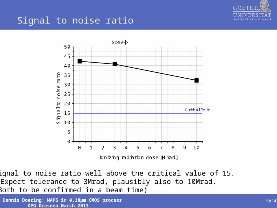
Signal to noise ratio
Dennis Doering: MAPS in 0.18µm CMOS process DPG Dresden March 2013 11
Signal to noise ratio well above the critical value of 15.Þ Expect tolerance to 3Mrad, plausibly also to 10Mrad.(Both to be confirmed in a beam time)
0 1 2 3 4 5 6 7 8 9 100
5
10
15
20
25
30
35
40
45
50
Sig
na
l to
no
ise
ra
tio
Ionizing radiation dose [Mrad]
Critical limit
Sr-90-

/17/14
Beam test result by IPHC Strasbourg
Dennis Doering: MAPS in 0.18µm CMOS process DPG Dresden March 2013 12
15 3095
96
97
98
99
100
De
tect
ion
eff
icie
ncy
[%
]
Temperature [°C]
Non-irradiated
1Mrad & 1013neq
/cm²
Pixel pitch: 20x40µm²Integration time: 32µs
Pion beam@SPS
MIMOSA-32 L4_1
CMOS 0.18µm process
CBMSIS100
0.18µmMIMOSA-32
Rad. hard. non-io. >1013 neq >1013 neq
Rad. hard. io > 1 Mrad > 1Mrad
Radiation hardness requirements of CBM@SIS100 achieved by MIMOSA-32.

/17/14
Summary
Dennis Doering: MAPS in 0.18µm CMOS process DPG Dresden March 2013 13
MAPS implemented in a smaller (0.18µm) feature size CMOS process.
- Noise of 0.18µm is still higher than known from 0.35µm. - Possible Origin identified, optimization is ongoing.
- Sufficient radiation tolerance for CBM@SIS100 was demonstrated in a beam test.
- Noise of only ~30e and S/N>30 (MPV) observed after 10Mrad. - Sufficient for excellent detection efficiencies for MIPS (to be confirmed in beam test).
- Next steps:
Add on-chip data sparsification circuits without losing radiation tolerance.

/17/14
Conclusion
Dennis Doering: MAPS in 0.18µm CMOS process DPG Dresden March 2013 14
High-resistivity
Smaller feature size
Radiation damage: Ionizing
Radiation damage: Non-ionizing

/17/14
Progress in sensor development
Dennis Doering: MAPS in 0.18µm CMOS process DPG Dresden March 2013 15
CBMSIS100
MAPS*(2003)
Single point res. ~ 5 µm 1.5 µm
Material budget < 0.3% X0 ~ 0.1% X0
Rad. hard. non-io. >1013 neq 1012 neq
Rad. hard. io > 1 Mrad 200 krad
Time resolution < 30 µs ~ 1 ms
*Optimized for one parameter

/17/14
Non-ionizing radiation: High-resistivity
Dennis Doering: MAPS in 0.18µm CMOS process DPG Dresden March 2013 16
0 5 10 15 20 25 30 35 401011
1012
1013
1014
1015
MIMOSA-18AHR* (2011)
MIMOSA-9
MIMOSA-9
MIMOSA-15 (2006)MIMOSA-18 (2008)
Sensor based on low-resistivity EPI layer
Ra
dia
tion
to
lera
nce
[n
eq/c
m²]
Pixel pitch [µm]*operated at -34°C
Preliminary
Sensor based on high-resistivity EPI layer
Shown:DPG Mainz 2012 HK 12.8Paper in preparation for publication
High resistivity epitaxial layer increases radiation hardness by one order of magnitude

/17/14
Ionizing radiation: 0.18µm process
Dennis Doering: MAPS in 0.18µm CMOS process DPG Dresden March 2013 17
15 3095
96
97
98
99
100
De
tect
ion
eff
icie
ncy
[%
]
Temperature [°C]
Non-irradiated
1Mrad & 1013neq
/cm²
Pixel pitch: 20x40µm²Integration time: 32µs
Pion beam@SPS
MIMOSA-32 L4_1
CMOS 0.18µm process
CBMSIS100
0.18µmMIMOSA-32
Rad. hard. non-io. >1013 neq >1013 neq
Rad. hard. io > 1 Mrad > 1Mrad

/17/14
Progress in sensor development
Dennis Doering: MAPS in 0.18µm CMOS process DPG Dresden March 2013 18
CBMSIS100
MAPS*(2003)
MAPS* (2012)
Single point res. ~ 5 µm 1.5 µm 1 µm
Material budget < 0.3% X0 ~ 0.1% X0 ~ 0.05% X0
Rad. hard. non-io. >1013 neq 1012 neq >3·1014 neq
Rad. hard. io > 1 Mrad 200 krad > 1 Mrad
Time resolution < 30 µs ~ 1 ms ~ 25 µs
*Optimized for one parameter
High-resistivity
0.18µm process
0.18µm process
See: HK 9.5 Mo 12:15: Dennis Doering: MAPS in 0.18µm process
This Session

/17/14Dennis Doering: MAPS in 0.18µm CMOS process DPG Dresden March 2013 19
High-resistivity
0.18µm process

/17/14
CMOS Monolithic Active Pixel Sensors
Dennis Doering: MAPS in 0.18µm CMOS process DPG Dresden March 2013 20
CBMSIS100
MAPS(2003)
0.35µm(2010)
Single point res. ~ 5 µm 1.5 µm 4 µm
Mat. budget [X0] < 0.3% ~ 0.1% ~ 0.05%
Rad. hard. non-io. [neq/cm²] >1013 1012 >1013
Rad. hard. io. [krad] > 1 000 200 > 500
Time resolution < 30 µs ~ 1 ms 110 µs

/17/14
CMOS Monolithic Active Pixel Sensors
Dennis Doering: MAPS in 0.18µm CMOS process DPG Dresden March 2013 21
CBMSIS100
MAPS(2003)
0.35µm(2010)
0.18µm(2012)
Single point res. ~ 5 µm 1.5 µm 4 µm
Mat. budget [X0] < 0.3% ~ 0.1% ~ 0.05%
Rad. hard. non-io. [neq/cm²] >1013 1012 >1013
Rad. hard. io. [krad] > 1 000 200 > 500 Smaller oxid layers
Time resolution < 30 µs ~ 1 ms 110 µs More complex logic possible

/17/14
Ionizing rad. Damage: Signal to Noise ratio
Dennis Doering: MAPS in 0.18µm CMOS process DPG Dresden March 2013 22
P1 P2 P3 P4 P5 P6 P7 P8 P9 P100
10
20
30
40
+20°C -20°C
Sig
na
l to
No
ise
Matrix
10MradSr-90
Dennis Doering
Preliminary
Critical limit
Signal to Noise ratios seem sufficient even after 10Mrad

/17/14
Open issues: Noise tails
Dennis Doering: MAPS in 0.18µm CMOS process DPG Dresden March 2013 23
Mi32TER
0 10 20 30 40 50 60 70 80 90 1001
10
100
En
trie
s
Noise [e]
0.35 µm 0.18µm
Dennis Doering
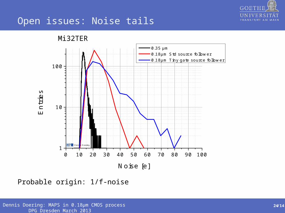
/17/14
Open issues: Noise tails
Dennis Doering: MAPS in 0.18µm CMOS process DPG Dresden March 2013 24
Mi32TER
0 10 20 30 40 50 60 70 80 90 1001
10
100
En
trie
s
Noise [e]
0.35 µm 0.18µm Std source follower 0.18µm Tiny gate source follower
Dennis Doering
Probable origin: 1/f-noise

/17/14
Deep Pwell: PMOS-transistors possible
Dennis Doering: MAPS in 0.18µm CMOS process DPG Dresden March 2013 25
0 20 40 60 80 100 120 140 160 180 2000
200
400
600
800
1000
1200
1400
1600
1800 Undefined state Low state High state
Mi32terP7 "seed"
Yie
ldCharge collected [ADC]
Dennis Doering
No change in charge spectrum observed, Þ It is allowed to operate a PMOS transistors without drawbacks in charge collection
P7: deep pwell everywhere
Mi32TER
Deep P-Well
DiodePMOS-Transistor(simplified)
d

/17/14
0 25 50 75 100 125 150 175 200 225 2500
200
400
600
800
1000
1200
1400
1600
NO deep Pwell Deep Pwell: d=6µm Deep Pwell: d=10µm
Mi32ter+20°C "seed"no clamp
Yie
ld
Charge collected [ADC]
Dennis Doering
Deep PWell hampers charge collection, reduces depleted zone of diode.Recovered for d=10µm:
Size of the diode hole?
Dennis Doering: MAPS in 0.18µm CMOS process DPG Dresden March 2013 26
Mi32TER
Deep P-Well
DiodePMOS-Transistor(simplified)
d

/17/14
Ionizing rad. damage: Response to MIPs
Dennis Doering: MAPS in 0.18µm CMOS process DPG Dresden March 2013 27
0 50 100 150 200250 300 350400 450 500550 600
20
40
60
80
100
120
140
160
180
200 +20°C unirradiated +20°C 3Mrad -20°C 3Mrad
Mi32 P6
Yie
ld
Charge collected [ADC]
Dennis Doering
As expected: No influence on the response
Zeigen?

/17/14
Noise and fake hit rate
Dennis Doering: MAPS in 0.18µm CMOS process DPG Dresden March 2013 28
P4 P2 P6 P51,801,851,901,952,002,052,102,152,202,252,302,352,402,452,50
-70°C -20°C +20°C
No
ise
[A
DC
]
Decreasing transistor size
Dennis Doering
P4 P2 P6 P51E-5
1E-4
1E-3 -70°C -20°C 20°C
Fa
ke h
it ra
teDecreasing transistor size
Dennis Doering
Threshold: 5 x noise
Noise increases with decreasing transistor size.Fake hit rates increases despite of noise adapted thresholds => Non GaussianNo clear temperature trend=>1/f noise?
Mi32TER
ELT Std Small Tiny
SF Transistor sizeELT Std Small Tiny
SF Transistor size

/17/14
Vary the transistor size
Dennis Doering: MAPS in 0.18µm CMOS process DPG Dresden March 2013 29
Mi32TER
0 50 100 150 200 250 3001E-10
1E-9
1E-8
1E-7
1E-6
1E-5
1E-4
1E-3
0,01
P5 Tiny P6 Small P2 Std. P4 ELT
Fak
e hi
t rat
e
Applied threshold [e]
Dennis Doering
-20°C

/17/14Dennis Doering: MAPS in 0.18µm CMOS process DPG Dresden March 2013 30
Deep P-Well
DiodePMOS-Transistor(simplified)
d
0 25 50 75 100 125 150 175 200 225 2500
200
400
600
800
1000
1200
1400
1600
P2 Reference P6 Small transistor P7 as P6, but Deep pwell small hole P8 as P6, but deep pwell large hole
Mi32ter+20°C "seed"no clamp
Yie
ld
Charge collected [ADC]
No DPWelld= 6µmd=10µm
For d=6µm, the depletion depth and the CCE is slighly reducedMostly recovered for d=10µm

/17/14Dennis Doering: MAPS in 0.18µm CMOS process DPG Dresden March 2013 31
0 10 20 30 40 50 60 70 80 90 1001
10
100
Entrie
s
Noise [e]
Mi18AHR A2 Mi32ter P2 Std. Mi32ter P5 Tiny SF
Dennis Doering
0 20 40 60 80 100 120 140 160 180 2000
200
400
600
800
1000
1200
1400
1600
1800 -20°C No clamping -20°C Low clamping -20°C High clamping
Mi32terP7 "seed"
Yie
ld
Charge collected [ADC]
Dennis Doering

/17/14
Fake hit rate (transistor size)
Dennis Doering: MAPS in 0.18µm CMOS process DPG Dresden March 2013 32
0 50 100 150 200 250 3001E-10
1E-9
1E-8
1E-7
1E-6
1E-5
1E-4
1E-3
0,01
P5 Tiny P6 Small P2 Std. P4 ELT
Fake
hit
rate
Applied threshold [e]
Dennis Doering
-20°C
Small transistor => dramatically higher fake hit rate

/17/14
A possible explanation
Dennis Doering: MAPS in 0.18µm CMOS process DPG Dresden March 2013 33
0 1 2 3 4 5 6 7 80
10
20
30
40 P2 Std.
P5 Tiny
Ent
ries
Noise [ADC]
-70°C
Dennis Doering
NP
ixel p
er b
in
hottest pixel ~50e
hottest pixel > 80e
Small gate => wide noise distribution => many hot pixels
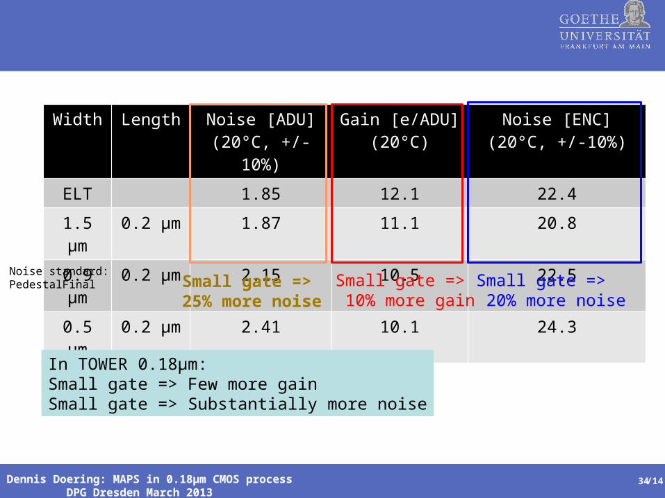
/17/14Dennis Doering: MAPS in 0.18µm CMOS process DPG Dresden March 2013 34
Width Length Noise [ADU](20°C, +/-10%)
Gain [e/ADU](20°C)
Noise [ENC](20°C, +/-10%)
ELT 1.85 12.1 22.4
1.5 µm 0.2 µm 1.87 11.1 20.8
0.9 µm 0.2 µm 2.15 10.5 22.5
0.5 µm 0.2 µm 2.41 10.1 24.3
Small gate => 10% more gain
Small gate =>25% more noise
Small gate => 20% more noise
Noise standard:PedestalFinal
In TOWER 0.18µm: Small gate => Few more gainSmall gate => Substantially more noise

/17Dennis Doering: MAPS in 0.18µm CMOS process DPG Dresden March 2013 35/14
Applications of MAPS
Picture STAR
Picture CBM
International Linear ColliderCBM-Experiment (FAIR, GSI)
STAR-Experiment
MAPS are developed for applications as vertex detector since 1999 at IPHC (Strasbourg).

/17/14
Operation principle
Dennis Doering: MAPS in 0.18µm CMOS process DPG Dresden March 2013 36
SiO2
N+ P+
P-
P+
Sensing diode
Epitaxial Layer
P-Well
Substrate
N+
50 µm
~50 µm thin sensors low material budget ⇒High granularity good spatial resolution ⇒
10-40 µm => a few µm resolution

/17/14
Operation principle
Dennis Doering: MAPS in 0.18µm CMOS process DPG Dresden March 2013 37
SiO2
N+ P+
P-
P+
Epitaxial Layer
P-Well
Substrate
e-
N+
e-
Particle
Sensing diode

/17/14
Non-ionizing radiation effects:Signal response
Dennis Doering: MAPS in 0.18µm CMOS process DPG Dresden March 2013 38
SiO2
N+ P+
P-
P+
Epitaxial Layer
P-Well
Substrate
N+
e-
Sensing diode
Defects

/17/14
Signal response
Dennis Doering: MAPS in 0.18µm CMOS process DPG Dresden March 2013 39
0 200 400 600 800 1000 1200 1400 1600 1800 20000
500
1000
1500
2000
2500
3000
3500
4000
4500
En
trie
s [1
bin
=4
AD
C]
Charge collected [e]
Unirradiated
Irradiated ( 3·1014neq
/cm2 )
MIMOSA-18 AHR 10µm Ru-106-T= -34°C
MPV: (591 ± 4) e(491 ± 20) e

/17/14
Non-ionizing radiation effects: Leakage current/Noise
Dennis Doering: MAPS in 0.18µm CMOS process DPG Dresden March 2013 40
SiO2
N+ P+
P-
P+
Epitaxial Layer
P-Well
Substrate
N+
--
Sensing diode
Defects
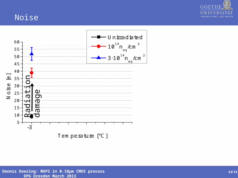
/17/14
5
10
15
20
25
30
35
40
45
50
55
60
No
ise
[e]
Temperature [°C]
Unirradiated
1014neq
/cm2
3·1014neq
/cm2
-3
Noise
Dennis Doering: MAPS in 0.18µm CMOS process DPG Dresden March 2013 41
Rad
iatio
nda
mag
e

/17/14
5
10
15
20
25
30
35
40
45
50
55
60
No
ise
[e]
Temperature [°C]
Unirradiated
1014neq
/cm2
3·1014neq
/cm2
-3
Noise
Dennis Doering: MAPS in 0.18µm CMOS process DPG Dresden March 2013 42
Rad
iatio
nda
mag
e

/17/14
5
10
15
20
25
30
35
40
45
50
55
60
-34-27-15
No
ise
[e]
Temperature [°C]
Unirradiated
1014neq
/cm2
3·1014neq
/cm2
-3
Noise
Dennis Doering: MAPS in 0.18µm CMOS process DPG Dresden March 2013 43
Rad
iatio
nda
mag
e
Cooling
2 times higher noise with respect to unirradiated

/17/14
Non-ionizing radiation effects
Dennis Doering: MAPS in 0.18µm CMOS process DPG Dresden March 2013 44
SiO2
N+ P+
P-
P+
Epitaxial Layer
P-Well
Substrate
N+
e-
--
Sensing diode
Defects

/17/14
Non-ionizing radiation effects
Dennis Doering: MAPS in 0.18µm CMOS process DPG Dresden March 2013 45
SiO2
N+ P+
P-
P+
Epitaxial Layer
P-Well
Substrate
N+
e-
--
Radiationdamage
Sensing diode
Defects

/17/14
Non-ionizing radiation effects
Dennis Doering: MAPS in 0.18µm CMOS process DPG Dresden March 2013 46
SiO2
N+ P+
P-
P+
Epitaxial Layer
P-Well
Substrate
N+
e-
--
Radiationdamage
Sensing diode
Defects

/17/14
Signal to Noise ratio
Dennis Doering: MAPS in 0.18µm CMOS process DPG Dresden March 2013 47
0 5 10 15 20 25 300
10
20
30
40
50
60
70
80
20µm (operated at room temp.) 10µm (operated at -20°C)
Sig
na
l to
No
ise
Radiation dose [1013neq
/cm2]
S/N limit (MIPS)
Technical feasible limits reached:- Pixel pitch- Operating temperature
Region of interest
?

/17/14
High-resistivity
Dennis Doering: MAPS in 0.18µm CMOS process DPG Dresden March 2013 48
Larger depleted volumes guided charge collection ⇒ ⇒ Improved charge collection efficiency (CCE)
SiO2
N+ P+
P-
P+
Epitaxial Layer
P-Well
Substrate
depleted volume
Low-resistivity High-resistivity
High-resistivity: Decrease of doping concentration in epitaxial layer.
Sensing diode

/17/14
Signal response
Dennis Doering: MAPS in 0.18µm CMOS process DPG Dresden March 2013 49
0 200 400 600 800 1000 1200 1400 1600 1800 20000
500
1000
1500
2000
2500
3000
3500
4000
4500
En
trie
s [1
bin
=4
AD
C]
Charge collected [e]
Low resistivity unirradiated
MIMOSA-18 AHR 10µm Ru-106-T= -34°C MPV: (293 ± 5) e

/17/14
Signal response
Dennis Doering: MAPS in 0.18µm CMOS process DPG Dresden March 2013 50
More charge collected in a high resistivity epitaxial layer.
0 200 400 600 800 1000 1200 1400 1600 1800 20000
500
1000
1500
2000
2500
3000
3500
4000
4500
En
trie
s [1
bin
=4
AD
C]
Charge collected [e]
Low resistivity unirradiated High resistivity unirradiated
MIMOSA-18 AHR 10µm Ru-106-T= -34°C MPV: (293 ± 5) e
(591 ± 4) e

/17/14
Signal response
Dennis Doering: MAPS in 0.18µm CMOS process DPG Dresden March 2013 51
Radiation damage effect after 3·1014neq/cm²: Some signal get lost due to recombinations. However, the high resistivity sensor is even irradiated better than the low resistivity sensor unirradiated.
0 200 400 600 800 1000 1200 1400 1600 1800 20000
500
1000
1500
2000
2500
3000
3500
4000
4500
En
trie
s [1
bin
=4
AD
C]
Charge collected [e]
Low resistivity unirradiated High resistivity unirradiated
High resistivity 3·1014neq
/cm2
MIMOSA-18 AHR 10µm Ru-106-T= -34°C MPV: (293 ± 5) e
(591 ± 4) e(491 ± 20) e

/17/14
Improvements using high resistivity
Dennis Doering: MAPS in 0.18µm CMOS process DPG Dresden March 2013 52
0 5 10 15 20 25 300
10
20
30
40
50
60
70
80
Low-resistivity 20µm (operated at room temp.) Low-resistivity 10µm (operated at -20°C) High-resistivity 10µm (operated at -34°C)
Sig
nal to
Nois
e (R
u-1
06
)
Radiation dose [1013neq
/cm2]
Error bars: Signal fit uncertainty * 10% noise uncertainty
*Beam test is pending
S/N limit (MIPS)
*
Parameters:- Pixel pitch- Operating temperature- Resistivity of epitaxial layer

/17/14
How to improve the non-ionizing radiation hardness of MAPS:- Operate the sensor at low temperature ( -30°C)- Small pixel pitch ( 10µm)- High-resistivity epitaxial layer (used here 400 Ωcm)
Conclusion
Dennis Doering: MAPS in 0.18µm CMOS process DPG Dresden March 2013 53

/17/14
How to improve the non-ionizing radiation hardness of MAPS:- Operate the sensor at low temperature ( -30°C)- Small pixel pitch ( 10µm)- High-resistivity epitaxial layer (used here 400 Ωcm)
⇒ Radiation hardness beyond 3·1014neq/cm²
Conclusion
Dennis Doering: MAPS in 0.18µm CMOS process DPG Dresden March 2013 54