1 – parts of the kit & tools required bugbrand workshop
TRANSCRIPT

BugBrand Workshop Oscillator MachineVersion3.1 October 2010
Welcome!
We're going to put together a little circuit board noise machine and, along the way, get anintroduction to some electronics and soldering techniques.
Don't worry if you've never done any electronics before – many people with zero priorknowledge have successfully built this machine in only a few hours. Also, while this handoutcontains quite a lot of information, much of it may go over your head for now – electronicscan be seriously confusing to begin with (I certainly found this!), but hopefully you can comeback to this information at a later date and gradually the pieces should begin to make sense.It is also fine, of course, just to build the machine and enjoy it!
All the parts are included in the kit – all you need is a soldering iron, some solder and a pairof wire cutters (more details in Sections 1).
The machine we'll make contains: Three oscillators – the sound sources A mixer – to blend the oscillators together Simple tone control – to shape the sound Jack output and mini-amp Circuit bends – 11 body contacts + power starvation
Parts of this document:1. The parts of the kit & tools required2. Soldering & building3. Examination of the circuit workings4. Further reading & final notes
Plus in the separate document: Full Schematic // Parts Placement // Large image of Completed Board // Bill of Materials
(Note – Version 3.0 was done Nov2009 and most of the photos were taken then so somepictures are very slightly different from the kits today!)
If you have questions while building, probably the best place to ask is on the Muff WigglerForum Thread: http://www.muffwiggler.com/forum/viewtopic.php?p=25190 Or you can contact me directly: [email protected]
Good Luck!& thanks!
Tom Bugswww.bugbrand.co.uk
The documents (in colour) can be downloaded from here:http://www.bugbrand.co.uk/docs/bugbrand_WOM_main.pdfhttp://www.bugbrand.co.uk/docs/bugbrand_WOM_schem_bom.pdf
1 – Parts of the kit & tools required
Carefully open up the main bag of parts – be careful as there are some small bits within! I'drecommend that you don't open up the smaller inner bags for now – wait until the buildingstage. Let's examine what we've got:
Contents (from top left): Resistors, Capacitors, ICs + Holders, PCB, Dials, Switches +Speaker, Battery + Holder
You may want to have the circuit schematic sheet on hand now so you can begin to comparethe parts discussed with what is drawn in the schematic – we'll introduce some symbols andterminology. By the way, a schematic is just a diagrammatic representation of the electroniccircuit – it shows which parts connect together, though it doesn't show the actual layout ofthe printed circuit board (PCB) – more on that later. Let's also note that much of thisintroduction is quite specific to this kit but should still be relevant to electronics in general.
We'll begin with the Battery (which comes with a holder and bolt to attach theholder). This will be the power for the circuit – the battery is a 9volt supply and we'lluse the terminology of V+ for the positive connection and Ground (Gnd) for thenegative connection. On the main schematic all points with the Gnd symbol arephysically connected together in the circuit (and the same for the V+ points).
Now take the Resistor bag (which also contains a couple ofdiodes). Resistors oppose the flow of electrical current andcome in many different values measured in Ohms (Ω) or, moreusually, thousands of Ohms – kilohms (kΩ) – or even millionsof Ohms – megohms (MΩ). By the way, we usually write 4700ohms as 4k7 (we know that they're in ohms so there's no needto write the Ω symbol). If you look closely you will see variouscoloured bands around each resistor – these identify theparticular value, and we'll examine these in the next section(note – to avoid confusion, keep the resistors on the paperstrips until you're about to use them!). Resistors are non-polarized components– it doesn't matter which way around they go.
In the bag there are also two types of Diode – these allow current to flow in one directiononly. Note the black ring around one end as this shows which way around to use them. Thesmaller diodes are 1N4148 silicon diodes which are commonly used, while the large one is a1N4001 rectifier diode which we'll use to provide battery polarity protection.

On to the Capacitors – there are three types ofvarious values in the bag. Capacitors (or caps)store electrical energy and are measured infractions of Farads – our typical values are inpicofarads (pF), nanofarads (nF) and microfarads(µf or uf) - 1000pF equals 1nF and 1000nF equals1uf. We have two types of low value caps here –the blue dipped-ceramic and the yellow polyester-box type (these types are pretty similar for ourpurposes) – note that these types are both non-polarized. There are also the black cylindrical electrolytic caps. These ones are polarizedand must be used the correct way around – they have a positive side (the straight line on theschematic symbol and the long leg on the actual cap) and a negative side (the short leg onthe cap – also there is a white stripe on this side with a minus symbol). We'll discuss moreabout the use of these capacitors when we look at the circuitry in the next section.
The next parts to consider are the chips or Integrated Circuits (ICs). These come in a littlepiece of foam along with IC holders for them – ICs can be sensitive (to heat or staticelectricity) so we generally attach a holder to the PCB first and only add the ICs once thecircuit is complete (this also allows easy replacement if something breaks). There are literallythousands of different types of ICs available today and within the fairly nondescript blackpackages they actually contain miniatureelectronic circuits (composed of parts likeresistors, capacitors, transistors etc). ICs have anumber of pins (or legs) – typically 8 or 14 in ourtypes of circuit – and these must be connected theright way around for correct operation (indeed, achip will likely be killed if connected the wrong wayaround!). Examining an IC you will notice a notchat one end (or sometimes just a dot) – the pin tothe left of this is Pin1 and the numbering from heregoes down that side and then up the other. It isbeyond our scope to look into the vast variety ofchip functions available, but let's look at one typethat we're using and see how the package andschematics hook up.
The two 14pin ICs we have are actually quitesimilar to one another – they are both members ofthe 4000 series CMOS Digital Family. One of thebest ways to find out information about an IC is togo to Google and search for the datasheet. We'lllook at the 4069 so you could search for '4069Datasheet'. We see that this chip is called a Hex Inverter – hex means it contains sixsections (gates) and the sections function as Inverters. Looking at the Pin Connectiondiagram you can see how the six sections connect to the pins of the chip. Two pins are leftover and these are the power pins – pin7 is labeled Vss and this connects to Gnd, whilepin14 is called Vdd and will connect to V+. The scheme of having the Gnd pin at bottom rightand V+ pin at top left is actually universal throughout the 4000series CMOS family. Also notethat the Pin Connection for the 40106 happens to be very similar to the 4069 – it is a HexSchmitt Inverter and also has 6 sections connected in the same way, but the sectionsprovide slightly different functions from the 4069.
The next bag contains the dials or Potentiometers(Pots). These are parts we use to control thebehaviour of the circuit. While the ones we're usingare small, they're pretty much the same as big dialson HiFi systems or synths. Pots are variableresistive elements with three pins and we'll usethem in one of two ways. The first way (shown onthe right) is called a Potential Divider (you cancheck Wikipedia for a more detailed explanation).There is a fixed value resistance between the outerpins (1 and 3) and then a wiper that movesbetween them as you move the dial. The way shown is used to attenuate a signal – ie as avolume control – turned one way the full signal is passed while turning the other way willmake no signal pass. The second application involves tying two of the pins together to givea variable resistor, a useful means of controlling the behaviour of a circuit – more details onthis in the circuitry section.
The last bag contains the final parts including theswitches which allow us to select different behaviours.Mechanical switches are common in day to day life soshould require little introduction. These particular oneshave three terminals (the other legs are just for addingstability) – when the switch is pushed one way then pins1 & 2 are connected together, while the other wayconnects pins 2 & 3, thus allowing us to select different routes within the circuitry.
There's not much left to examine – the Speaker should beself-explanatory but lets just look at the Jack Socket. This isa switched mono 1/4” socket (ie for standard guitar cable). Ithas four legs, two on each side. The signal goes out on tothe tip of the jack plug and the sleeve connects to the circuitGnd. Note also that when no jack plug is inserted the legs oneither side are connected – this allows us to automaticallyswitch off the mini-speaker when a cable is plugged in.When the plug is inserted the horizontal pieces of metal arelifted up and thus the legs on the lower side are left unconnected.
Finally lets take a quick look at the Printed Circuit Board (PCB). This has been specificallydesigned for this project – laid out directly from the schematic diagram and fabricated in afar-away land! Its actually quite a complex procedure to do such a design and for most one-off circuits you'd simply use a material called stripboard (look it up) but for replicatableprojects it really makes sense – everything is laid out nicely and building errors areminimized. If you examine the PCB you'll see tracks on the top and bottom of the boardjoining the different parts together. The gold coloured pads for the components makesoldering easy (hopefully!). Now, people have asked why we make this project directly on thePCB without using a box. I've found that these on-board-circuits are strong and reliable. Thetime saved by avoiding putting it in a box is quite considerable and it also makes the projecta good deal less complicated. Over the years I've been building things I've found that themost time consuming part of making devices is the boxing – wiring up pots and othercontrols. The wiring is also a place were faults can easily develop and my aim for this projecthas really been to make something that is almost guaranteed to work first time – the onething that kills a buzz for electronics really quickly is when you finish building something andthen it doesn't work!

ToolsThere's another factor in my choice of mounting everything on the PCB – hardly any toolsare required for the building! All that is required is a soldering iron (plus stand), something forcleaning the soldering iron (either a dampened sponge or brass wool tip cleaner), somesolder (naturally!) and a pair of wire cutters (ideally a small pair though larger ones will dothe job). There are more notes on soldering and where to get an iron at the end of thisdocument in the appendix – have a check!
It is worth just mentioning how to set up a place to work – clear a good area so that thingswon't get lost (as mentioned before, keep things in their bags until you're going to use them)and find yourself a good source of light as you will find it extremely hard to solder withoutenough light to see what you're doing! It's also worth locating yourself somewhere with goodventilation, perhaps next to an open window – while the fumes from soldering aren'thazardous some people find them irritating.
2 – Soldering & BuildingIn the interest of keeping things interesting (!) we're going to move straight on to buildingbefore examining the workings of the circuit – but we'll come back to that in the next section.
First let's talk about soldering. This is an area that often puts people off electronics, but witha little info its actually very straight forward! Bad soldering is probably the largest factor incrushing the enjoyment of electronics! Poor techniques will result in bad joints which don'twork or are intermittent – so pay close attention to the soldering and your project shouldwork first time.
It should go without saying that the iron is HOT and should be handled with care both toavoid burning yourself and items / people around you!
Soldering is a process where a metal alloy (solder) is melted to join metal surfaces together.For this we need heat – provided by the soldering iron. When you're starting out there reallyis no need to shell out on an expensive iron – all the irons I use in my teaching workshopscost under £5 (off eBay) and work just fine. What IS important is to keep the tip of the ironclean – a dirty tip, even on a decent iron, won't allow good soldering!
Cleaning – a clean tip should appear shiny. If the tip is dull / dark grey then it needs to becleaned before soldering. The tip of a hot iron will gradually oxidize forming a thin layer ofoxide over the tip which isn't good for heat transfer. We use a cleaning sponge or brass-woolcleaner to remove this layer and then melt a little solder onto the iron tip (a process knownas tinning). After this the tip should appear nice and shiny – if not, repeat the cleaningprocess another time. The iron's tip should always be tinned when sitting in its holder – Ialways clean and re-tin the tip when I put down the iron after soldering and then clean itagain when I pick it up.
Soldering – the aim of soldering is to heat up both the component lead and the PCB pad.Once they're heated enough, solder is melted onto the join and it flows around thecomponent lead to form a solid seal. We must do this relatively quickly to prevent damage tothe component or board (certainly no longer than 5seconds but preferably around 1second).We need to apply enough solder to fully cover the seal, but not too much as to make abulbous joint (as this can hide problems). The join should appear clean and shiny – not a dullgrey – and should be slightly concave.

So, follow this order each time: Clean the tip Tin the tip Heat the joint of lead and pad Flow the solder [Solder further joints if required, cleaning the tip as necessary (c. every 5 – 10 joints)] Clean and re-tin the tip before replacing the iron in its holder
You may also want to think about how you hold the iron and how you position your hands forthe work. I hold the iron in my right-hand (as I am right-handed!) and then the lower side ofmy hand rests on the desk – this gives a very stable position for working. I then turn the PCBin whatever direction is needed to get good access to the point of soldering. The left-hand ismulti-tasking – I use it to feed solder into the join and sometimes use my fingers to hold thePCB steady at the same time.
If you do notice a bad joint then it is always possible to reflow the solder and fix the problem– either just reheat the joint until it flows properly or desolder it and reapply fresh solder.
Just a couple of notes on solder - firstly, while solder used to generally contain Lead (apoisonous metal) most of Europe now uses Lead-Free solder due to the RoHS (Restrictionof Hazardous Substances) Directive. My PCBs are all made to Lead-free standards and allcomponents I supply are also Lead-free. Also note that solder wire generally contains a coreof a substance called flux – a chemical cleaning agent that facilitates soldering. This cansometimes splutter a little when soldering and may leave a little residue around the solderjoint (which isn't generally a problem – but it can be cleaned off if required). Flux is alsoresponsible for the smoke that occurs when soldering – this smoke is generally harmless butmay cause some respiratory irritation, especially for asthmatics, so if possible worksomewhere with good ventilation (by a fan or window).
Desoldering – if you make a mistake you may have to remove some solder and this isactually a little tricky with these fabricated PCBs – so try to avoid mistakes in the first place!There are two methods possible – a solder-sucker or desoldering braid.
A solder-sucker is vacuum pump which sucks up molten solder. You depress the plunger,use the iron to melt the solder to be removed, place the tip of the sucker by the melted jointand then press the button to suck. Unfortunately, this technique tends not to work so well onfabricated PCBs due to the though-hole plating.
Desoldering braid draws up molten solder bycapillary action. You put the braid on top of the solderto be removed and press the iron tip on top, meltingthe solder into the braid. It is generally necessary topull the braid across the join to remove all the solder– a technique that takes a little practice!
Ok – finally the time comes to build...(you may want to turn on your soldering iron at this point to let it heat up)
But first: Don't rush! Double check everything before soldering – ask if you have problems!
Better to move slowly than to make errors. Keep that iron clean!
Proceeding in a methodical manner is of vital importance – do things by stages so that youdon't confuse yourself and to avoid components getting mixed up (keep things in their bagsuntil you'll use them). We generally build from lowest profile (height) component upwards –so we start with resistors and move from there. It may be a good idea to work along with theBill of Materials sheet (BOM) as this lists the components in the order you'll put them in. Youmay like to cross the items off as you solder them in place.
We'll start with the two small silicon diodes – examine them and observe the black bandaround one end. Now locate the positions for D1 and D2 on the PCB and note that there's aline marked on them – this shows the correct orientation of the diodes (these are polarizedcomponents and must go the correct way around). You will also notice that one pad is round,the other is square – the band on the diode should go to the square hole. Remove one of thediodes from the paper strip and bend the leads at right-angles as shown – the bends shouldbe tight to the body so the diode will fit snuggly into the PCB and fit right up to the board.
Turn the board over making sure the diode stays in position – you can splay the legs outslightly to prevent the component moving about. Now have a go at soldering, rememberingthe order: clean tip -> tin tip -> heat join -> flow solder -> clean, tin and replace. If all goescorrectly you should have two nice clean solder joints. If you've done that ok then you cansnip the leads off just above the join – nice and neat.
Do the same for the other diode – hopefully you'll be getting a feel for how the solder andiron work and feel... From there we move to the resistors – you may prefer at this point tostart placing several components at a time before soldering them all. Though – don't putthem all in at once or you'll find all the legs get in the way!

While most circuits will make use of a wide varietyof resistor values, this kit is designed with simplicityin mind so we've only got three different values. Asmentioned, the coloured bands on the resistor'sbody show the resistance value – do a Googlesearch for more information. The resistors we usehave the following colours:
• 1K: Brown/Black/Black/Brown/Brown• 10k: Brown/Black/Black/Red/Brown• 1M: Brown/Black/Black/Yellow/Brown
As you can see, all the colours are the sameexcept for the fourth band as the resistors are allmultiples of 100 ohms. (remember that 1M means1000K). You may prefer just to keep the resistors attached to the paper strips and figure outthe values by deduction – there's just one 1M, two 1Ks and ten 10Ks.
Let's begin with the 1Ks (R10 & R12) and the single 1M (R9) located as shown below. Do theusual steps of bending the legs close to the body, put them in place and solder. Note thatresistors are not polarized – it doesn't matter which way around they go. I find when I'msoldering that I turn the board round to find the best way to get the iron tip to the solder joint.Also be careful not to inadvertently solder up any extra holes with a careless movement ofthe iron!
To finish up the resistors we fill up all the remaining spaces with the ten 10Ks – R1, R2, R3,R4, R5, R6, R7, R8, R11, R13:
We finish off these first steps by adding the power diode (D90) to the top left corner of theboard, by the battery box and the On/Off switch.
Hopefully all your resistors and diodes are now in place and properly soldered!
Next come the holders for the ICs which are held in the piece of foam (note: NOT the actualICs!). You should have one 8pin socket and two 14pin ones. Note the notch at one end ofeach holder and, identifying the placements IC1-3, line up the holders with the PCBmarkings. Now – you'll probably notice that when you turn the PCB upside down to continuesoldering that all the IC holders fall out! I suggest holding the holder in place with a finger,turning the board upside down and then bending out a pin on each side to hold the holder inplace before soldering (do this one by one for each IC holder).
Before soldering make absolutely sure that all the legs have correctly gone through theirholes (sometimes legs get bent under the holder) – if you start soldering before noticing sucha problem then you've got a right task trying to desolder things and sort out the problem! Andmake sure you solder all the pins – don't inadvertently miss any!

Capacitors come next – find the bag and empty them out. There are three types – there's asingle blue dipped ceramic, various yellow or blue poly-boxes and the black towerelectrolytics. We'll put each group in separately, so start with the blue ceramic (C4). You maynotice that numbers are printed on the side (maybe hard to read!) - it should say 103 whichmeans 10 plus Three Zeroes – ie: 10,000pF or 10nF.
Note that the ceramic and polybox caps are not polarized – they can go in either wayaround, so locate the positions, put the caps in, solder and trim....
On to the poly box caps. These have a slightly confusing number system (this actually variesa lot between different types and makes of capacitor) so make sure to sort them out correctlyusing the pictures below as a guide. There are two blue boxes – the small one is the 10n cap(for the Tone control) while the big one is the 680n (marked on the cap as u68). The single22n, 47n and 470n are quite clearly marked on top, but the 100n and 220n (4 of these) areconfusing as these are written .1 and .2. By the way, the extra letters/numbers indicate themaximum voltage rating for these caps (63v or 100v).It is important that you identify the caps correctly as otherwise the WOM may workstrangely – double check with the picture below before soldering!
Now, the final electrolytic caps are polarized and so must be put in the correct way around(they can pop if connected back-to-front!). If you examine them you will see that:
the value and voltage rating are marked in small letters on the side (eg 100u 10v –you can ignore the voltage marking)
next to this is a vertical white(ish) strip with minus signs marked – this shows thenegative lead which will go to the round pad
the legs are also of different lengths – the short one corresponds to negative and thelonger one is positive (goes to the square hole)
If it is hard to read the numbers off the side you can probably identify the different caps byprocess of elimination! There are two small 4u7 caps (C9 and C91), one slightly larger 100ucap (C10) and then one much larger 470u cap (C90) – we'll keep C90 off for now due to itslarger size. Remember – the long lead goes to the square hole!
Time for the controls – the pots. You can leave off the spindle dials until the end, so put themback in the bag and sort out the different value pots. There should be two marked as 10k(Tone and Level) and then seven remaining all with 1M (OSC1-3, LVL1-3, Starve).
You'll probably find that, like the IC holders, the pots often don't want to stay in place beforesoldering, so here's a technique. Begin with just one pot for example one of the 10Ks to go inthe Tone position. Firstly, hold the pot roughly in position with a finger and turn the boardupside down. We want to just tack a little solder onto one of the legs to hold the pot in place– it doesn't matter if the pot is slightly out of position for now. With the pot held roughly, pickup the board, still keeping it upside down, and put a finger of your left hand onto the pot fromunderneath. While pressing on the pot, reflow the single solder connection until it melts – atthis point the pot (which you're pressing) will pop into the correct position! Once that's done,you can solder the remaining legs. Use the same technique for the other 10K pot and then fillthe other spaces with the 1M ones.
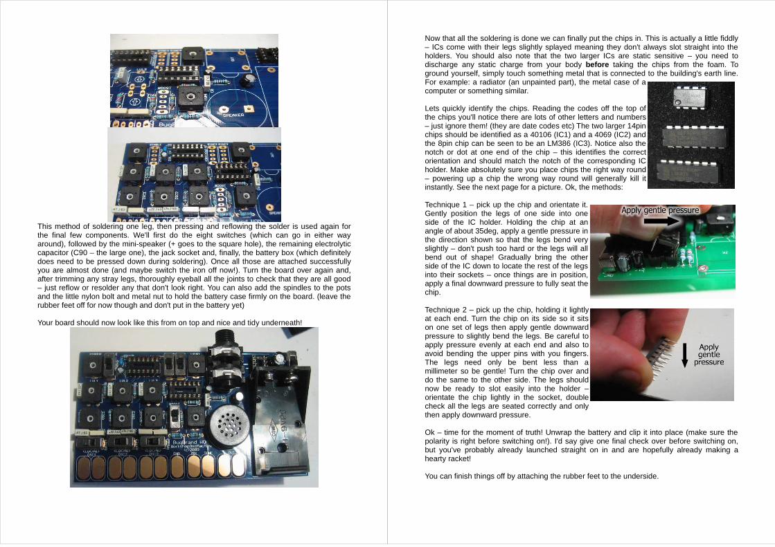
This method of soldering one leg, then pressing and reflowing the solder is used again forthe final few components. We'll first do the eight switches (which can go in either wayaround), followed by the mini-speaker (+ goes to the square hole), the remaining electrolyticcapacitor (C90 – the large one), the jack socket and, finally, the battery box (which definitelydoes need to be pressed down during soldering). Once all those are attached successfullyyou are almost done (and maybe switch the iron off now!). Turn the board over again and,after trimming any stray legs, thoroughly eyeball all the joints to check that they are all good– just reflow or resolder any that don't look right. You can also add the spindles to the potsand the little nylon bolt and metal nut to hold the battery case firmly on the board. (leave therubber feet off for now though and don't put in the battery yet)
Your board should now look like this from on top and nice and tidy underneath!
Now that all the soldering is done we can finally put the chips in. This is actually a little fiddly– ICs come with their legs slightly splayed meaning they don't always slot straight into theholders. You should also note that the two larger ICs are static sensitive – you need todischarge any static charge from your body before taking the chips from the foam. Toground yourself, simply touch something metal that is connected to the building's earth line.For example: a radiator (an unpainted part), the metal case of acomputer or something similar.
Lets quickly identify the chips. Reading the codes off the top ofthe chips you'll notice there are lots of other letters and numbers– just ignore them! (they are date codes etc) The two larger 14pinchips should be identified as a 40106 (IC1) and a 4069 (IC2) andthe 8pin chip can be seen to be an LM386 (IC3). Notice also thenotch or dot at one end of the chip – this identifies the correctorientation and should match the notch of the corresponding ICholder. Make absolutely sure you place chips the right way round– powering up a chip the wrong way round will generally kill itinstantly. See the next page for a picture. Ok, the methods:
Technique 1 – pick up the chip and orientate it.Gently position the legs of one side into oneside of the IC holder. Holding the chip at anangle of about 35deg, apply a gentle pressure inthe direction shown so that the legs bend veryslightly – don't push too hard or the legs will allbend out of shape! Gradually bring the otherside of the IC down to locate the rest of the legsinto their sockets – once things are in position,apply a final downward pressure to fully seat thechip.
Technique 2 – pick up the chip, holding it lightlyat each end. Turn the chip on its side so it sitson one set of legs then apply gentle downwardpressure to slightly bend the legs. Be careful toapply pressure evenly at each end and also toavoid bending the upper pins with you fingers.The legs need only be bent less than amillimeter so be gentle! Turn the chip over anddo the same to the other side. The legs shouldnow be ready to slot easily into the holder –orientate the chip lightly in the socket, doublecheck all the legs are seated correctly and onlythen apply downward pressure.
Ok – time for the moment of truth! Unwrap the battery and clip it into place (make sure thepolarity is right before switching on!). I'd say give one final check over before switching on,but you've probably already launched straight on in and are hopefully already making ahearty racket!
You can finish things off by attaching the rubber feet to the underside.

What happens, though, if it doesn't work? That's a tricky one and frustrating too... There areseveral areas to start checking:
double check the orientation of the ICs and that the chips are in the correct positions. bad soldering – this is probably the most common mistake when starting out. Check
and check again that all the joints are good – it can often take a while to spot (maybetake a break and come back a bit later). Pay attention to joints that look overlybulbous, as underneath the solder it may be that the component isn't actually pokingthrough at all... If things look suspect then it may be good to desolder and thenresolder to be sure.
check also that all the leads are properly snipped close – I've seen short leads leftwhich then bend over to cause a short circuit.
In a similar manner, check that adjacent pads haven't been accidentally solderedtogether (something called a solder bridge) – again, desolder and repair when thingslook suspect.
Check all the solder joints once again!
Section 3 – Workings & CircuitryI always reckon that the best way to learn an instrument like this is to just dive in anddiscover! Controls are labeled (..a bit small perhaps..) so that may give some clues too. But,there'll come a time when you may want to know more. So lets look at the controls and thenat the circuitry that's making it all tick.
As described at the start, the circuit we've got contains:
3 Oscillators -> Mixer -> Tone Control -> Output -> Mini-Amp
The circuit board has been laid out in a way that is (hopefully!) quite logical – imagine thesignal flowing from left to right, beginning with the oscillators, mixing these and shaping thetones before outputting the sounds.
Oscillators: – Each has a Range switch (Lo rate = left, Hi rate = right), a Pitch dial and a Level
control that sets the volume to the mixer.– The Starve control effects all three Oscs by simulating the battery running out of
power. Turning the dial fully clockwise means full power. This is coupled with theStable switch which changes the behaviour when the power is starved.
– The Sync switches are used to 'synchronize' Oscs 2 & 3 to the rate of Osc1 to give arich harmonic sound (look on the Internet for more details on Sync!). Note that for anOsc to be sync'd it must be running at a higher pitch than Osc1 otherwise no soundwill be heard. It also works best when the Oscs are run at full power.
Mixer & Tone:– The three Osc signals are mixed via their Level controls. The mixer has a Boost
switch which changes its gain – this is especially useful when the Osc section ispower starved as the amplitude of the waveforms drops dramatically and this Boosthelps maintain a relatively stable output volume.
– The Tone control is a simple low-pass filter that cuts out treble frequencies. You maynot hear much with the onboard Mini-Amp but it is more noticeable when you plug intoan external sound system.
– You will find that the sound and behaviour change quite a lot dependent on how loudyou push things. The machine also becomes much more stable when sound is takenfrom the 1/4” output jack (which mutes the mini-amp) – though I really like thecharacter of the speaker sound!
Output & MiniAmp:– The 1/4” output jack can be used with a standard guitar cable to plug into an amp or
mixer – though note that the output signal can be loud! So begin with the volume low. – Plugging a jack into the output socket removes power from the Mini-Amp, thus
conserving battery power.– The Mini-Amp drives a miniature speaker to give portable sonic-fun! It can be quite
power hungry and the battery is used up fastest when volume is loudest. You'll hearhow the sound changes as you increase the volume due to the power use.
Other Bits:– The battery clip holds a standard 9v PP3 (square) battery. Due to the Touchplates you
should only ever use a battery to power the WOM – never use a DC power supplythat plugs into the mains!
– You should be aware that the battery contacts are exposed on the back of the PCB sobe careful of metal objects short-circuiting these points, especially during transport (itmay be best to remove the battery)

Touch Plates:– The Touch Plates connect straight to various points of the circuit and allow your body
to act as a variable resistive path between different stages. You are basically acting asa resistor between points – when your skin is dry your effective resistance may beseveral mega-ohms, while if you lick your fingers you will appear more like a low valueresistor.
– By touching several different points at the same time you are creating chaotic pathsfor signals to flow!
** **
Time now to get a closer look at the schematic – the scarily large diagram of components..The good thing is that we can actually break it down into several much more manageablechunks. This is often the way in circuitry – you take several building-blocks and group themtogether into a larger piece. Many of these building blocks can also be used on their own orregrouped in different ways. You can find a lot more info about things on the internet, inparticular by finding the datasheet for each chip which often contain functional data andexample circuits. If you don't know what a word means then look it up on Google!
Just remember – points on the schematic with the little downwards Gnd triangle are allconnected together (and the same for points with V+ or V_Strv) – it just makes it a lot clearernot to actually draw lines joining all the points together! Also note that when you see linescrossing on the page, they are only joined when there is a black dot – you can see these atmost junctions on the schematic, but can see some without the black dot (ie NO join) aroundthe Out jack.
Ok – let's start with the Oscs section which makesuse of the 40106 chip. This chip has a technicalname of Hex Schmitt Inverter (!) - this translates to achip which, internally, contains six (hex) SchmittTrigger gates. If we look at the 40106's datasheetwe can see the internal layout of the chip – what pindoes what. This chip can actually be made toproduce, very simply, six squarewave oscillators! Allyou need is a power source, six resistors and sixcapacitors. We, though, add a bit more on top togive more flexibility.
Let's look at the basic Osc setup, focusing just on the firstgate between pins 1 & 2. If we hook a resistor between pins1 & 2 and then a cap from pin 1 to ground, we'll get asquarewave output from pin 2 – simple as that! The speedor frequency of the squarewave depends on the values ofthe two components – a bigger capacitor gives slowerspeeds (and vice versa), and a large value resistor alsogives slower speeds.
This setup will just give us a fixed frequency output – to get a variable pitch we simplychange R1 from a fixed resistor to a variable one (we actually also add a small value fixedresistor so the overall resistance doesn't reach 0 ohms). Examine the main schematic andyou'll see that's how we've set up the Oscs – each one has a small value resistor (10K) plusa 1M variable resistor between the gate pins. We can then see that there are switches toselect between two different caps for each Osc – when switched to the smaller value capyou get a higher pitch range.
There's another part in the Osc section to consider – Sync. What we're doing here with C4,R4 and gate IC1F is to make a very narrow pulse from the Osc1 squarewave – this can thenbe used to reset the other oscillators (the Sync points on the schematic join up).
Finally, notice that two of the gates within the 40106 are not used (gates D & E). It iscommon practice to tie the inputs of any unused gates to ground – otherwise they canoscillate and cause unstable behaviour (maybe not a bad thing for our design, but we do itanyway for good practice!)
Most of the rest of the circuit is based around the 4069 chip – this is actually a really usefulchip that despite its humble appearance. The six internal Inverters can be used as a varietyof building blocks and we'll implement just a couple. Have a look online for further examplesusing this chip. You can again see that we've tied the unused gates to ground.
The Mixer uses one of the 4069 gates like a summing OpAmp (look it up!). The Levelcontrols are set up as Potential Dividers which control the amplitude of the Osc signalpassing in. We use decoupling capacitors (C5-7) to remove the DC offset as the Levelcontrols and Osc outputs are referenced to ground – we want the signals to 'float' around avoltage mid-point half-way between the V+ and Gnd powerlines.
If we examine an example setup, stripping away excess circuitry – the Gain of the mixer isdetermined by the ratio of the values of R_Input and R_Gain. If we have R_Input as thesame value as R_Gain then we get a Gain of 1 – ie the signal input is output with the sameamplitude. If we raise the value of R_Gain then the gain is increased and vice-versa. Wecould equally decrease the value of R_Input to increase the gain. Further signals can bemixed by adding further copies of R_Input – one resistor for each input. Generally you'll keepthe values of these input resistors the same, but if you wanted one input to generally belouder than another then you could use different values accordingly. Just to note also – theoutput signal is actually inverted in polarity – this won't affect you much, but it may beimportant to know this for future work.
So, looking back at the main schematic – we see the input resistors (R5-7) as 10K resistorsand we can use the Boost switch to select two different values of gain resistor. When the10K gain resistor is selected then the Mixer has unity gain of 1, while switching to the 1Mresistor increases the gain factor greatly by a factor of 100.
There is one other thing to consider – if we've got a gain factor of 100 then we may expectan input signal of 1volt to be output as 100volts. Unfortunately this isn't the case due to thefact that the chip is only powered by our 9v battery supply – this limits any amplification to amaximum of 9v. The interesting thing with the 4069 chip is that when you over-amplify asignal and drive it into the power-line limits you get a nice overdrive effect! While this isn't allthat noticeable here due to the squarewave signals we're generally dealing with, you coulduse a very similar circuit to create a simple guitar overdrive pedal.
There's also a simple tone control set up with the Tone pot and cap C8. This is a simple LowPass Filter – it attenuates the high frequency parts of the signal – dependent on theresistance and the capacitor value. Turning the dial to 0 ohm resistance (fully clockwise aswe've connected it) allows all frequencies to pass, while turning it to full 10k brings in the

filtering action. The value of C8 could be changed to alter the frequency range – increase thevalue for a lower cutoff frequency and vice versa.
The final stage around the Level control should be quite apparent – it is the same opamptype approach we used for the mixer, but this time we've only got one input signal and havea variable control to set the gain factor from 0 to 1.
We discussed the action of the Out jack a bit in the first section – when no cable is pluggedin, the signal passes straight through to the final Mini-Amp section and also the groundconnection is made. The LM386 is a simple little power amp chip used in the final Mini-Ampsection (a very standard setup is shown) – you can actually use a very similar setup to makea mini guitar amp head which can drive a full Marshall speaker cab.
Lets just finally look a little at the Power section. Each chip needs power to the appropriatepins and we generally add an electrolytic cap (C90) near the power input to stabilize thesupply and also a power diode to provide protection if the battery is inadvertently connectedbackwards.
By putting a variable resistor in series with the powerline we can create a starvation effect –this only works well, in this particular setup, effecting the supply to the 40106 Osc chip notthe rest of the circuit. With the starve pot turned fully clockwise there is no resistance acrossthe V+ line, so the chip gets the full supply, but as we turn the dial down the resistanceincreases and so the chip is starved. This sends things pretty crazy – the oscillators seem tofight amongst themselves, perhaps trying to gobble up the limited power available to sharebetween them! This starved power also has a stabilizing electrolytic cap that can be switchedin/out using the Stable switch – this cap (C91) behaves in a similar manner to C90 (the mainpower supply filter cap) and smooths the power line so you get less chaotic behaviour.
Ok – that was a very brief overview of the circuitry. As we said right at the start – you don'tneed to really understand what is going on to build or have fun with the circuit, but hopefullythis overview can give some directions if you want to find out more.
4 – Final & Further DetailsWell done if you've successfully built the Workshop Osc Machine! Hopefully you've enjoyedthe experience and picked up some useful skills along the way. While the workings of theelectronics may not be clear yet, you've hopefully realized that soldering isn't too tricky whenyou follow some basic approaches.
There is a wealth of further information available on the Internet and in your local library –dive in (if you want..) - it's the best way to learn!
Firstly a recommended book:Handmade Electronic Music (the Art of Hardware Hacking) by Nicolas CollinsThis book is very well regarded as a source of inspiring projects and information – coversmuch of what we've done and so much more!
Some useful / interesting websites:www.bugbrand.co.uk – the BugBrand website with many sounds and some further electronicbits'n'pieceswww.cadsoft.de – home of the software, Eagle, that I use for schematics and PCB layout. Afreeware version is availablehttp://electro-music.com/forum/index.php?f=112 – the EM DIY forum – a great place to askquestionshttp://www.muffwiggler.com/forum/index.php – the MuffWiggler forum – home to the W.O.M.discussion thread and a great source of synthnesshttp://makezine.com/ – a technological magazine and blog – their videos, projects and forumare worth a look for information
Parts:www.rapidonline.com – a really great place to get parts in the UK (much better prices andstock than M*plin!)www.futurlec.com – Thailand based webshop with very low prices (takes a while for deliverythough)www.mouser.com – good for the US
Further good electronics:www.musicfromouterspace.com – Ray Wilson's site has a load of great info and circuits. Inparticular there is another simple little project (with PCB available) called the Wacky SoundGenerator or you can get the more complex synth project, the SoundLab Mini-Synth.http://www.cgs.synth.net/modules/ - Ken Stone's synth designs – a bit more complex to build,but very high quality & lots of useful info – PCBs are available.http://www.geofex.com/ - lots of good info (but a bit all over the place)http://bleeplabs.com/thingamakit/ - Bleeplabs' fun project with light control chaos!