1 la electronics meeting, cascina, 25.01.2006 virgo alignment system overview ● linear alignment...
TRANSCRIPT
1 LA electronics meeting, Cascina, 25.01.2006
Virgo alignment systemoverview
● Linear Alignment principle● Optical configuration
● Present situation● Foreseen developments
2 LA electronics meeting, Cascina, 25.01.2006
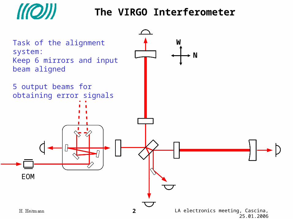
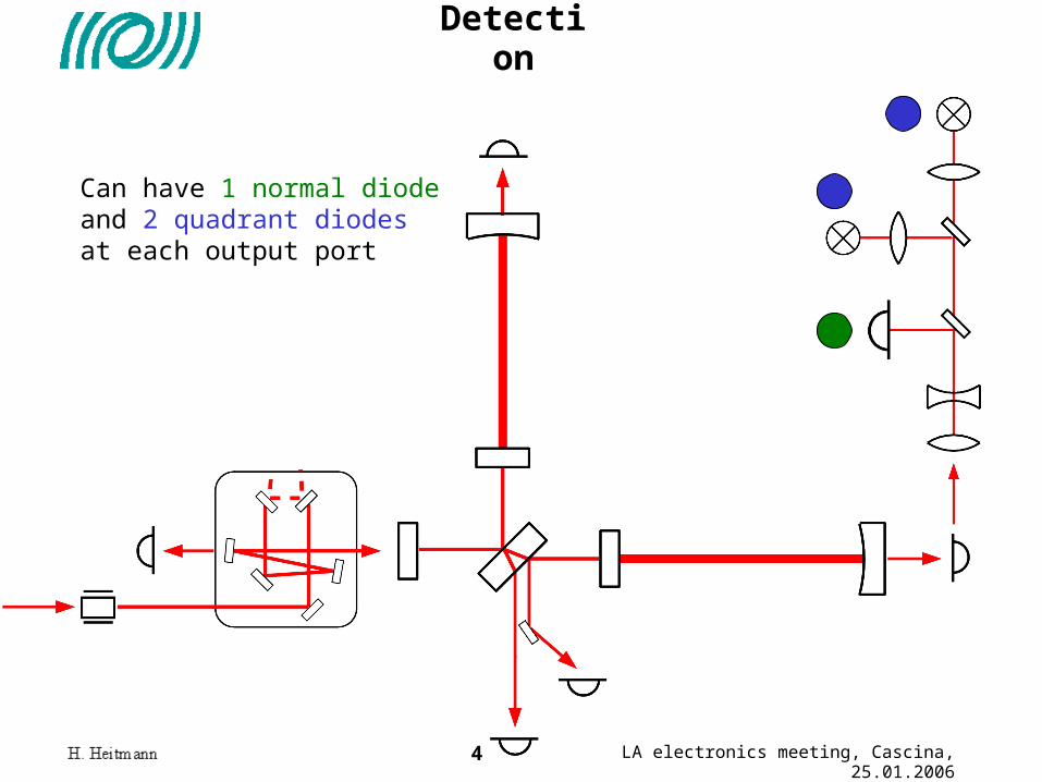
The VIRGO Interferometer
N
W
EOM
Task of the alignment system:Keep 6 mirrors and input beam aligned
5 output beams for obtaining error signals
3 LA electronics meeting, Cascina, 25.01.2006
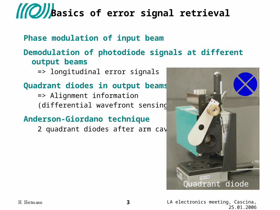
Basics of error signal retrieval
Phase modulation of input beam
Demodulation of photodiode signals at different output beams=> longitudinal error signals
Quadrant diodes in output beams=> Alignment information (differential wavefront sensing)
Anderson-Giordano technique2 quadrant diodes after arm cavities
Quadrant diode
4 LA electronics meeting, Cascina, 25.01.2006
Can have 1 normal diode and 2 quadrant diodes at each output port
Detection
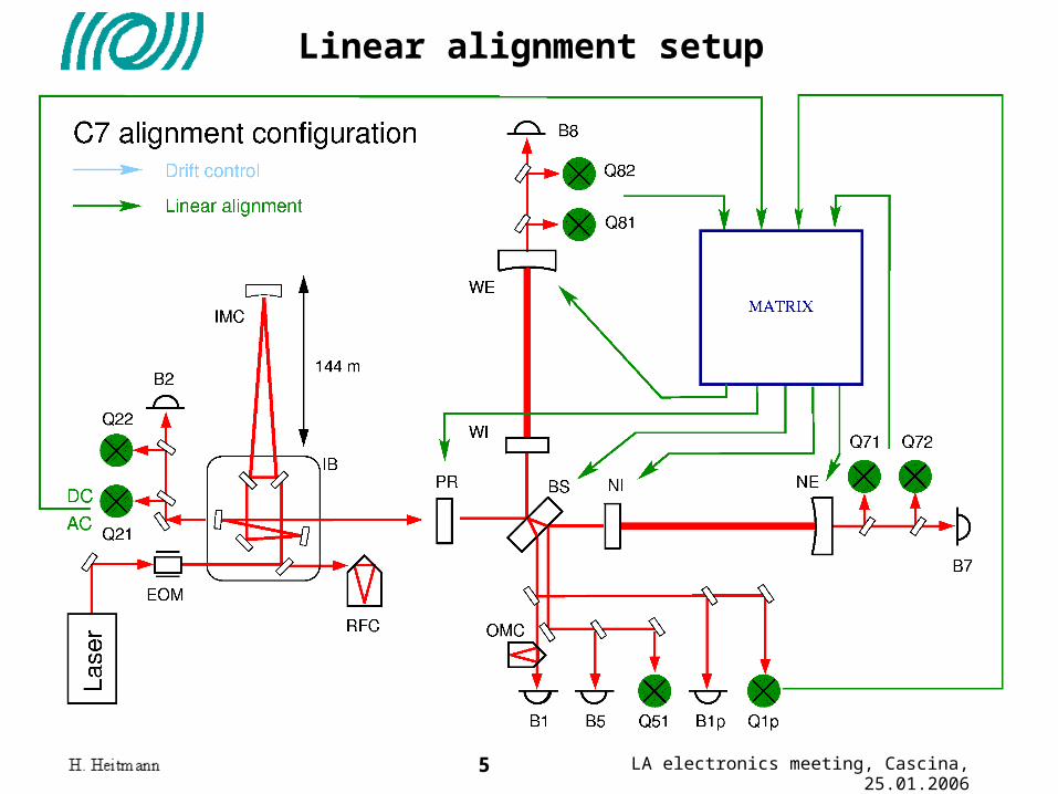
5 LA electronics meeting, Cascina, 25.01.2006
Linear alignment setup
6 LA electronics meeting, Cascina, 25.01.2006
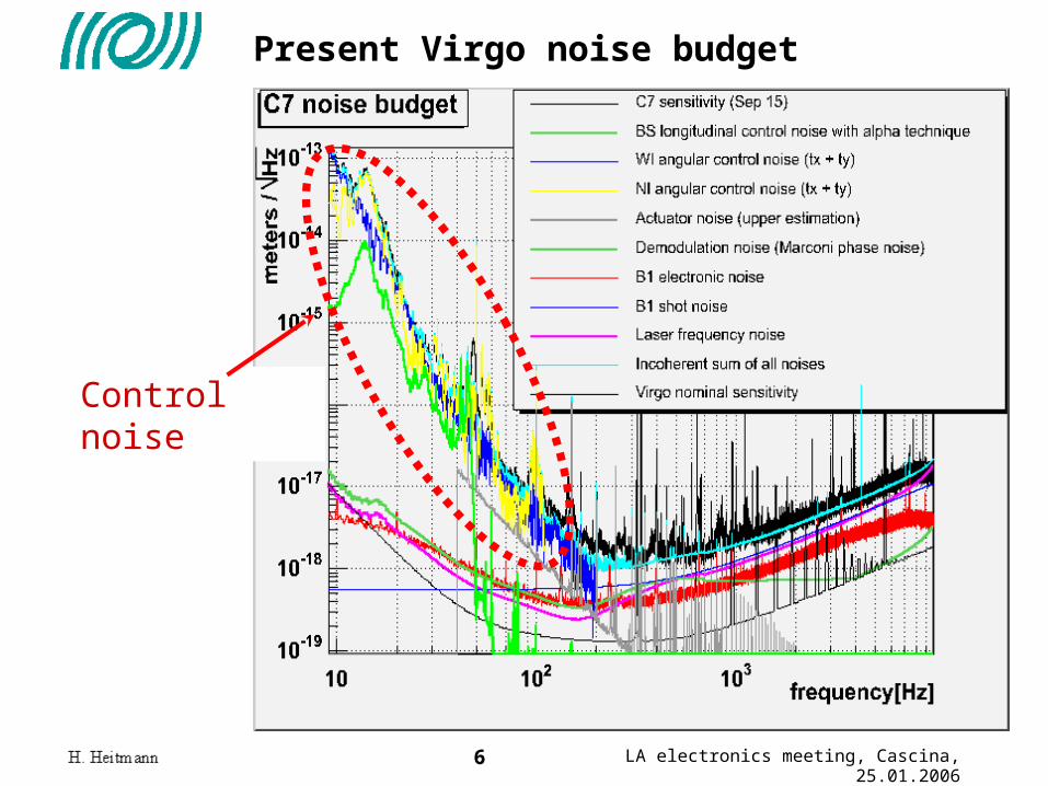
Control noise
Present Virgo noise budget
7 LA electronics meeting, Cascina, 25.01.2006
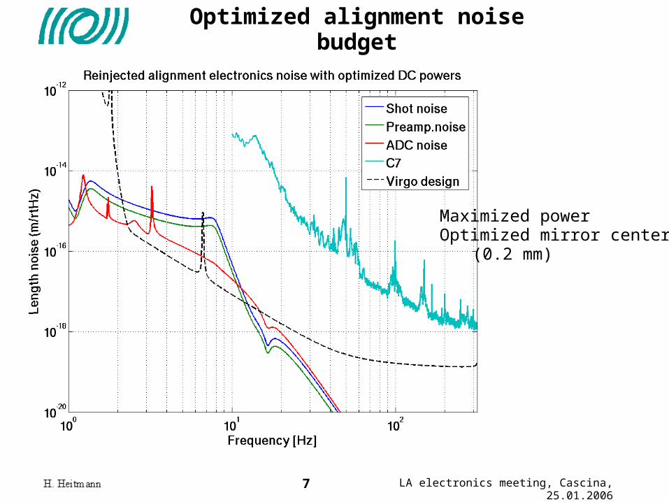
Optimized alignment noise budget
Maximized powerOptimized mirror centering
(0.2 mm)
8 LA electronics meeting, Cascina, 25.01.2006
Present situation
Frascati group is leaving VirgoSince 01/2006
Frascati’s responsibilitiesOriginal design of alignment system
Strategy, optics, prototype experiments, …
Design & realization of electronics
ProblemContinue support for alignment electronicsMake new modules / spare modulesContinue development for new requirements
9 LA electronics meeting, Cascina, 25.01.2006
Developments
Present developmentsMore modules needed
Installation of 9th quadrant diode (maybe 10th)Spares needed
New Annecy local oscillator boards, compatible with alignmentPhase shifters for standard photodiodes
Possible developmentsSubstitute Si diodes with InGaAs diodes
Better quantum efficiencyLower bias voltage
=> higher power capability lower noise
Reduction of electronics noiseBetter preamplifier: 5 pA/rtHz -> 1.6 pA/rtHz (?)DC signals: pre-amplification / pre-shaping
Fast quadrant centering system(Napoli is working on that)LA noise limits sensibility (especially at low frequ.)
End
11 LA electronics meeting, Cascina, 25.01.2006
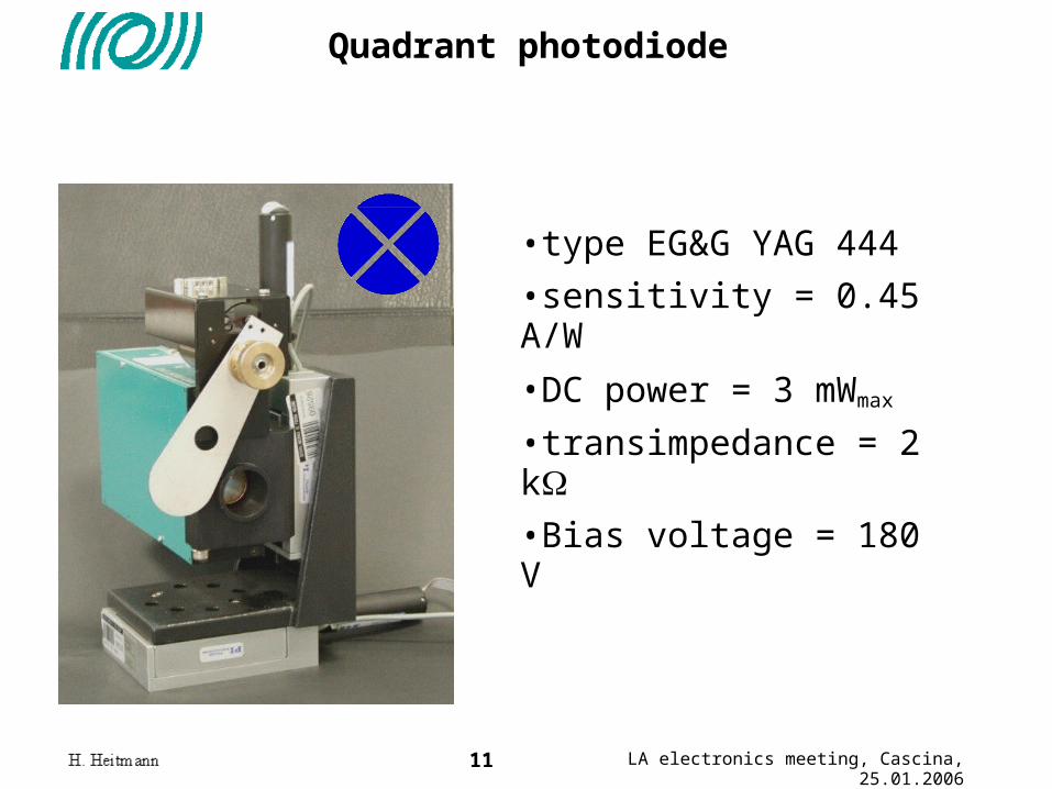
Quadrant photodiode
•type EG&G YAG 444
•sensitivity = 0.45 A/W
•DC power = 3 mWmax
•transimpedance = 2 k•Bias voltage = 180 V
12 LA electronics meeting, Cascina, 25.01.2006
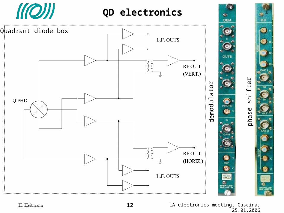
QD electronics
dem
odul
ator
phas
e sh
ifte
r
Quadrant diode box
13 LA electronics meeting, Cascina, 25.01.2006
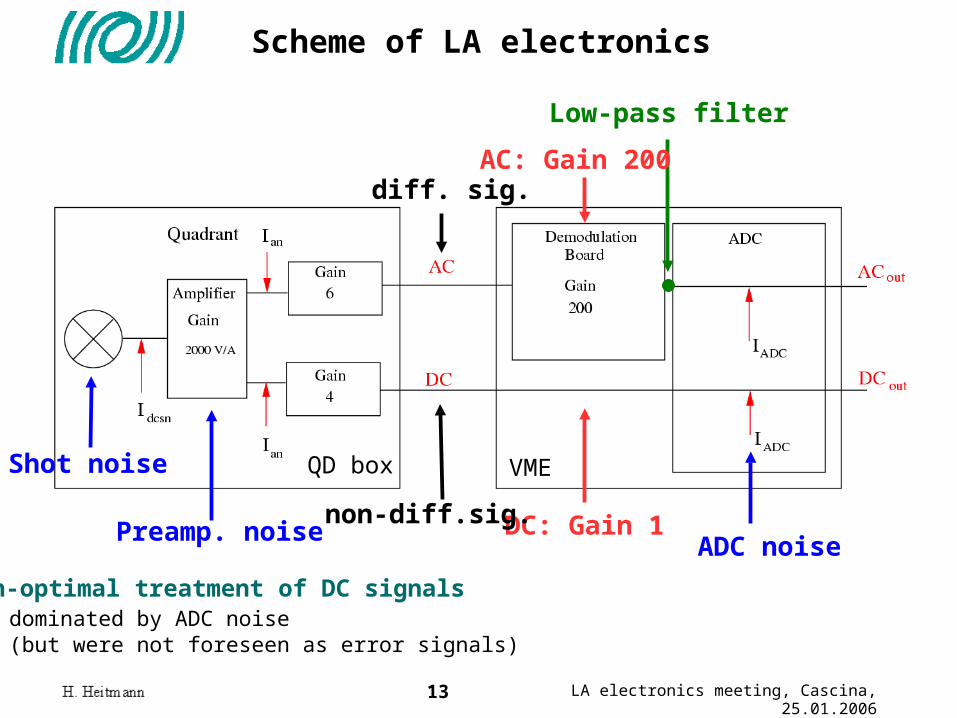
Scheme of LA electronics
ADC noisePreamp. noise
Shot noise
Low-pass filter
AC: Gain 200
DC: Gain 1
diff. sig.
non-diff.sig.
Non-optimal treatment of DC signalsdominated by ADC noise(but were not foreseen as error signals)
VMEQD box
14 LA electronics meeting, Cascina, 25.01.2006
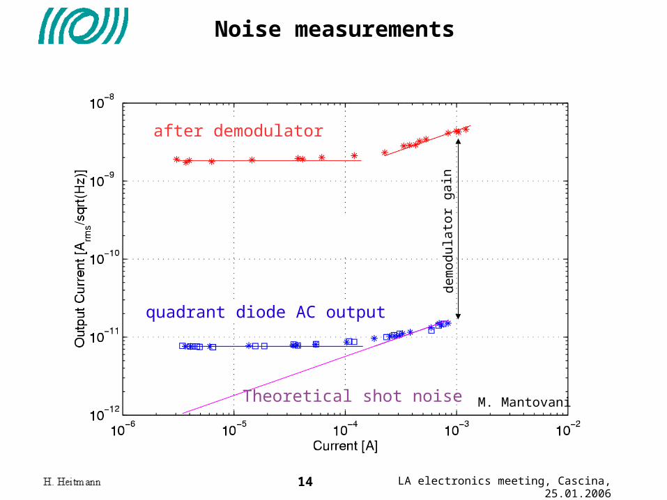
Noise measurements
after demodulator
quadrant diode AC output
Theoretical shot noise M. Mantovani
dem
odul
ator
gai
n
15 LA electronics meeting, Cascina, 25.01.2006
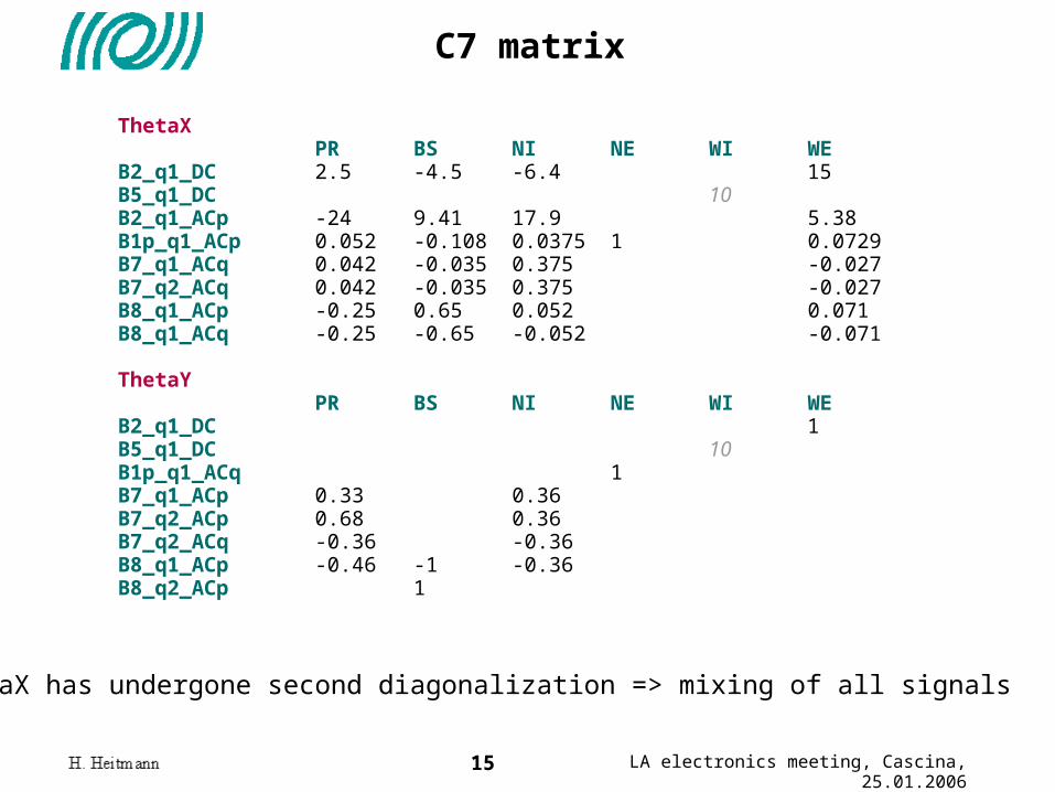
C7 matrix
ThetaX PR BS NI NE WI WEB2_q1_DC 2.5 -4.5 -6.4 15B5_q1_DC 10B2_q1_ACp -24 9.41 17.9 5.38B1p_q1_ACp 0.052 -0.108 0.0375 1 0.0729B7_q1_ACq 0.042 -0.035 0.375 -0.027B7_q2_ACq 0.042 -0.035 0.375 -0.027B8_q1_ACp -0.25 0.65 0.052 0.071B8_q1_ACq -0.25 -0.65 -0.052 -0.071
ThetaY PR BS NI NE WI WEB2_q1_DC 1B5_q1_DC 10B1p_q1_ACq 1B7_q1_ACp 0.33 0.36B7_q2_ACp 0.68 0.36B7_q2_ACq -0.36 -0.36B8_q1_ACp -0.46 -1 -0.36B8_q2_ACp 1
ThetaX has undergone second diagonalization => mixing of all signals
16 LA electronics meeting, Cascina, 25.01.2006
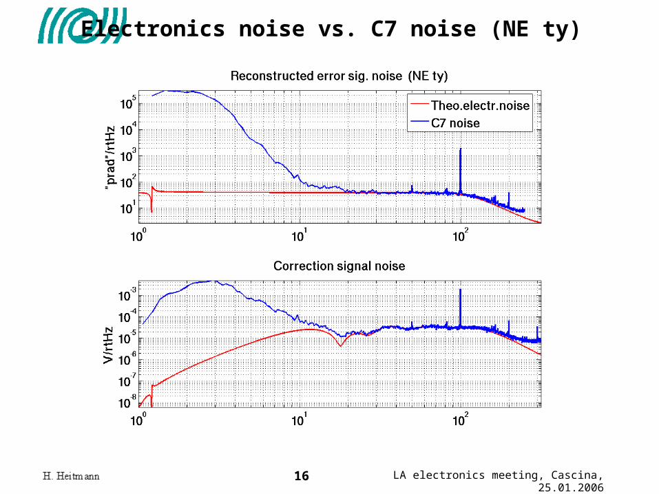
Electronics noise vs. C7 noise (NE ty)
17 LA electronics meeting, Cascina, 25.01.2006
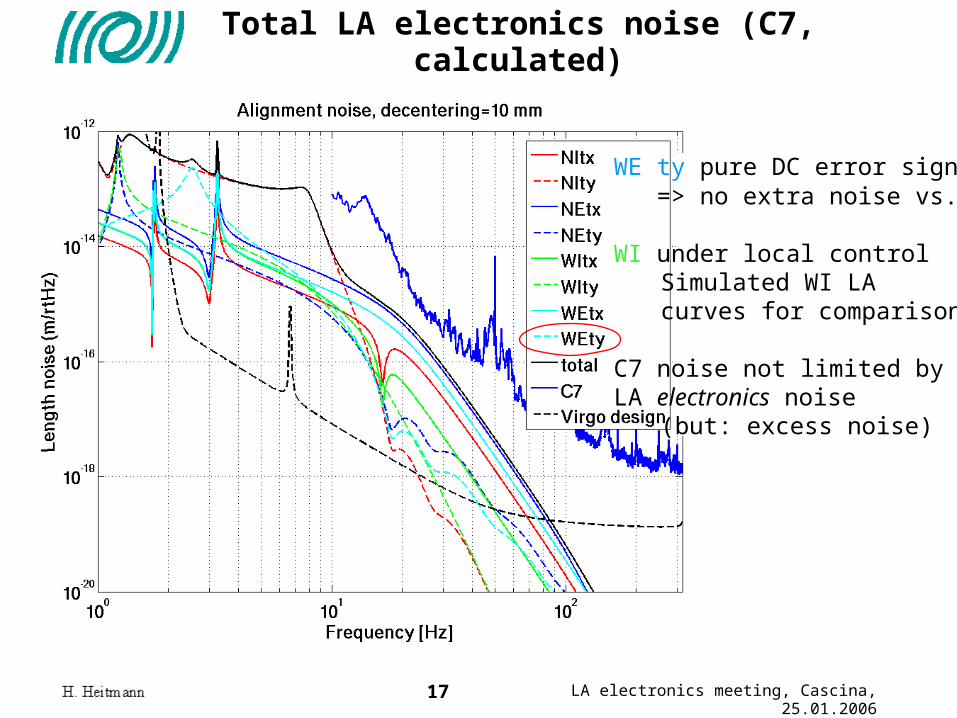
Total LA electronics noise (C7, calculated)
WE ty pure DC error signal => no extra noise vs. AC
WI under local controlSimulated WI LA curves for comparison
C7 noise not limited byLA electronics noise
(but: excess noise)
18 LA electronics meeting, Cascina, 25.01.2006
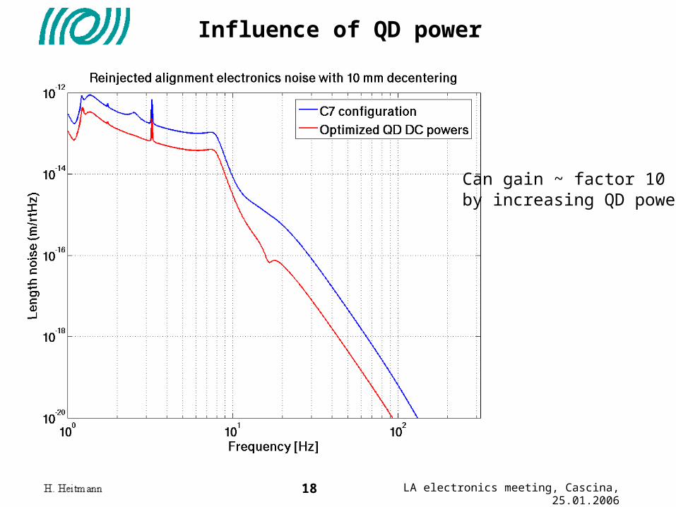
Influence of QD power
Can gain ~ factor 10by increasing QD powers