1-kw/36-v power stage for brushless motor in battery powered
TRANSCRIPT

Brushless
motor
Offset
Offset
OPA2374
3.3 V
PWMs
DRV8303
36 VLi-ion
battery
pack
SPI
Three-
phase
NMOS
gate
driver
Control
and
protection
Temperature sensor output
TPS54061
Voltage
divider
LMT84
Motor voltage feedback
Motor current
feedback
CSD18540Q5B (x6)
Input DC voltage feedback
C2
00
0 I
nsta
SP
IN-F
OC
La
un
ch
Pa
d I
nte
rfa
ce
Sh
un
t
Sh
un
t
Sh
un
t
TP
D4
50
09
(TV
S)
TI Designs1-kW/36-V Power Stage for Brushless Motor in BatteryPowered Garden and Power Tools
TI Designs Design FeaturesTI Designs provide the foundation that you need • 1-kW Power Stage With Field Oriented Control forincluding methodology, testing and design files to Permanent Magnet Synchronous Motorsquickly evaluate and customize the system. TI Designs • Designed to Operate from 10-Cell Li-Ion Batteryhelp you accelerate your time to market. Voltage Ranging from 30 to 42 V
• Delivers up to 30-ARMS Continuous Motor CurrentDesign ResourcesWith an Airflow of 400 LFM
Tool Folder Containing Design FilesTIDA-00285 • Small PCB Form Factor of 57 × 59 mm Using 60-V/400-APEAK, 1.8-mΩ RDS_ON, SON5x6 PackageCSD18540Q5B Product FolderMOSFETs for Power StageDRV8303 Product Folder
TPS54061 Product Folder • Uses DRV8303 Three-Phase Gate Driver, WhichCan Operate from 6 to 60-V Input, SupportingOPA2374 Product FolderProgrammable Gate Current With MaximumTPD4S009 Product FolderSetting of 2.3-A Sink / 1.7-A SourceLMT84 Product Folder
TMS320F28027F Product Folder • Overcurrent Protection Configurable for Cycle-by-Cycle Control or Latch ShutdownLAUNCHXL-F28027F Tool Folder
• Sense Feedback of Individual Phase Voltage, DCBus Voltage, and Low-Side Current on Each Phase
ASK Our E2E Experts for Sensorless ControlWEBENCH® Calculator Tools • Can Support Brushless DC Motor Control Using
Trapezoidal Method• 3.3-V/0.15-A Step-Down Buck Converter forFeatured Applications
Powering MCU• Power Tools
• Designed to Operate at an Ambient Temperature of• Garden Tools –20°C to 55°C• Lawn Mover Robots• Vacuum Cleaning Robots
All trademarks are the property of their respective owners.
1TIDU708–February 2015 1-kW/36-V Power Stage for Brushless Motor in Battery Powered Garden andPower ToolsSubmit Documentation Feedback
Copyright © 2015, Texas Instruments Incorporated

Introduction www.ti.com
An IMPORTANT NOTICE at the end of this TI reference design addresses authorized use, intellectual property matters and otherimportant disclaimers and information.
1 IntroductionThis reference design is a power stage for brushless motors in battery-powered garden and power toolsrated up to 1 kW. The power stage operates from a 10-cell lithium-ion battery with a voltage range from 36to 42 V. The design uses CSD18540Q5B NexFETs featuring a very low drain-to-source resistance(RDS_ON) of 1.8 mΩ in a SON5x6 SMD package, which results in a very small form factor of 57 × 59 mm.The three-phase gate-driver DRV8303 is used to drive the three-phase MOSFET bridge, which canoperate from 6 to 60 V and support programmable gate current with maximum setting of 2.3-A sink / 1.7-Asource. The power stage can be configured for a single-shunt or three-shunt current sensing. The designsupports sensorless control for brushless DC (BLDC) and permanent magnet synchronous motors(PMSM) using trapezoidal control or field oriented control (FOC). The C2000™ Piccolo™ LaunchPad™ isused with the power stage to implement InstaSPIN™-FOC using the motor current and voltage feedback.The corresponding test report evaluates the thermal performance of the board and overcurrent protectionfeatures such as cycle-by-cycle control and latch control of the DRV8303.
Power tools are used in various industrial and household applications such as drilling, grinding, cutting,polishing, driving fasteners, various garden tools, and so on. The most common types of power tools useelectric motors while some use internal combustion engines, steam engines, or compressed air.
Power tools can be either corded or cordless (battery-powered). Corded power tools use the mains power(the grid power) to power up the AC or DC motors. The cordless tools use battery power to drive DCmotors. Most of the cordless tools use lithium-ion batteries, the most advanced in the industry. Lithium-ionbatteries have high energy density, low weight, and greater life. These batteries have relatively low self-discharge (less than half that of nickel-based batteries) and can provide a very high current forapplications like power tools. Cordless tools use brushed or BLDC motors. The brushless motors are moreefficient and have less maintenance, low noise, and longer life.
Power tools have requirements on form factor and thermal performance. Therefore, high-efficient powerstages with a compact size are required to drive the power tool motor. Small form factor of the powerstage enables design flexibility for optimal cooling method and placement of the power stage close to thebattery pack to minimize impedance on connections carrying high current. High efficiency providesmaximum battery duration and reduces cooling efforts. High efficiency requirement in turn asks forswitching devices with low RDS_ON. The power stage should also take care of protections like motor stall orany other chance of high current.
The objective of this reference design is to provide a 1-kW/36-V power stage for brushless motors used inbattery powered applications (like power tools, garden tools, and so on). This design demonstrates thepower stage in a small form factor (57 × 59 mm) operating from a 36-V DC input (using a 10-cell Li-ionbattery) and delivers up to 30-ARMS continuous current output to motor. The design also providesscalability for lower voltage and current levels. At higher power levels, the cooling is provided by forcedair, which allows for the small form factor.
2 1-kW/36-V Power Stage for Brushless Motor in Battery Powered Garden and TIDU708–February 2015Power Tools Submit Documentation Feedback
Copyright © 2015, Texas Instruments Incorporated
www.ti.com Key System Specifications
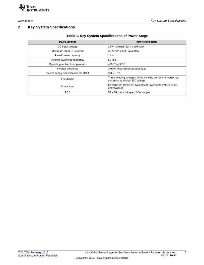
2 Key System Specifications
Table 1. Key System Specifications of Power Stage
PARAMETER SPECIFICATIONDC input voltage 36-V nominal (42-V maximum)
Maximum input DC current 30 A with 400 LFM airflowRated power capacity 1 kW
Inverter switching frequency 60 kHzOperating ambient temperature –20°C to 55°C
Inverter efficiency ≥ 97% (theoretical) at rated loadPower supply specification for MCU 3.3 V ±5%
Three winding voltages, three winding currents (inverter legFeedbacks currents), and input DC voltageOvercurrent (cycle-by-cycle/latch), over temperature, inputProtections undervoltage
PCB 57 × 59 mm / 4-Layer, 2-Oz copper
3TIDU708–February 2015 1-kW/36-V Power Stage for Brushless Motor in Battery Powered Garden andPower ToolsSubmit Documentation Feedback
Copyright © 2015, Texas Instruments Incorporated

System Description www.ti.com
3 System DescriptionCompared to their brushed motor counterpart, permanent magnet brushless motors are gainingimportance because of their high efficiency, low maintenance, high reliability, low rotor inertia, low noise,and so on. A brushless PMSM has a wound stator and a permanent magnet rotor assembly. Thesemotors generally use internal or external devices to sense rotor position. The sensing devices providelogic signals for electronically switching the stator windings in the proper sequence to maintain rotation ofthe magnet assembly. The sensor-based solution requires accurate mechanical assembly of sensors. Therotor position can also be estimated using sensorless algorithms implemented in microcontroller units(MCUs).
The electronic drive is required to control the stator currents in a brushless permanent magnet motor. Theelectronic drive consists of:• A power stage with three-phase inverter having the required power capability• MCU to implement the motor control algorithm• Motor voltage and current sensing for sensorless control and closed loop speed or torque control• Gate driver for driving the three-phase inverter• Power supply to power up the MCU
3.1 Brushless Permanent Magnet MotorsPermanent magnet motors can be classified based on Back-EMF (BEMF) profiles: brushless direct current(BLDC) motor and permanent magnet synchronous motor (PMSM). Both BLDC motors and PMSMs havepermanent magnets on the rotor but differ in the flux distributions and BEMF profiles. In a BLDC motor,the BEMF induced in the stator is trapezoidal, and in a PMSM, the BEMF induced in the stator issinusoidal. Implementation of an appropriate control strategy is required to obtain the maximumperformance from each type of motor.
4 1-kW/36-V Power Stage for Brushless Motor in Battery Powered Garden and TIDU708–February 2015Power Tools Submit Documentation Feedback
Copyright © 2015, Texas Instruments Incorporated
q
q
q
q
Ic
Ec
I
Eb
Ia
Ea
Phase C
Phase B
Phase A
Torque
www.ti.com System Description
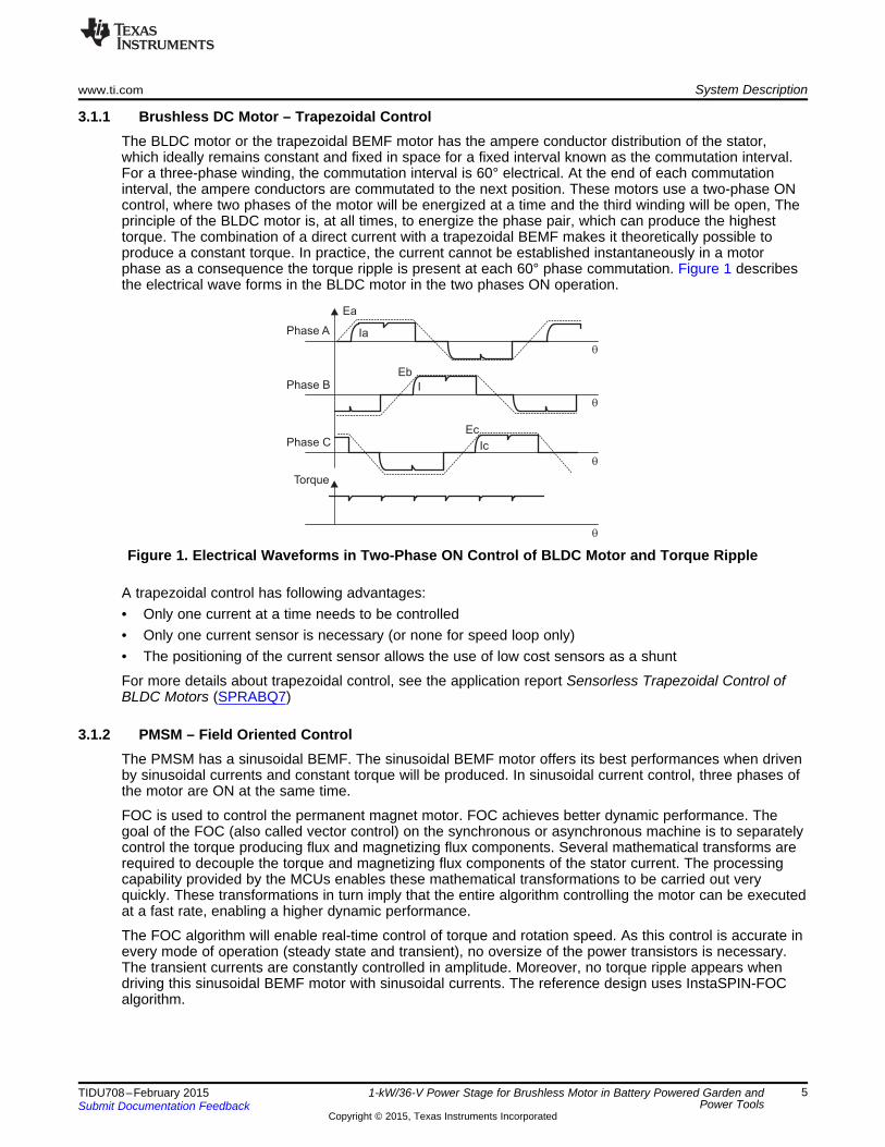
3.1.1 Brushless DC Motor – Trapezoidal ControlThe BLDC motor or the trapezoidal BEMF motor has the ampere conductor distribution of the stator,which ideally remains constant and fixed in space for a fixed interval known as the commutation interval.For a three-phase winding, the commutation interval is 60° electrical. At the end of each commutationinterval, the ampere conductors are commutated to the next position. These motors use a two-phase ONcontrol, where two phases of the motor will be energized at a time and the third winding will be open, Theprinciple of the BLDC motor is, at all times, to energize the phase pair, which can produce the highesttorque. The combination of a direct current with a trapezoidal BEMF makes it theoretically possible toproduce a constant torque. In practice, the current cannot be established instantaneously in a motorphase as a consequence the torque ripple is present at each 60° phase commutation. Figure 1 describesthe electrical wave forms in the BLDC motor in the two phases ON operation.
Figure 1. Electrical Waveforms in Two-Phase ON Control of BLDC Motor and Torque Ripple
A trapezoidal control has following advantages:• Only one current at a time needs to be controlled• Only one current sensor is necessary (or none for speed loop only)• The positioning of the current sensor allows the use of low cost sensors as a shunt
For more details about trapezoidal control, see the application report Sensorless Trapezoidal Control ofBLDC Motors (SPRABQ7)
3.1.2 PMSM – Field Oriented ControlThe PMSM has a sinusoidal BEMF. The sinusoidal BEMF motor offers its best performances when drivenby sinusoidal currents and constant torque will be produced. In sinusoidal current control, three phases ofthe motor are ON at the same time.
FOC is used to control the permanent magnet motor. FOC achieves better dynamic performance. Thegoal of the FOC (also called vector control) on the synchronous or asynchronous machine is to separatelycontrol the torque producing flux and magnetizing flux components. Several mathematical transforms arerequired to decouple the torque and magnetizing flux components of the stator current. The processingcapability provided by the MCUs enables these mathematical transformations to be carried out veryquickly. These transformations in turn imply that the entire algorithm controlling the motor can be executedat a fast rate, enabling a higher dynamic performance.
The FOC algorithm will enable real-time control of torque and rotation speed. As this control is accurate inevery mode of operation (steady state and transient), no oversize of the power transistors is necessary.The transient currents are constantly controlled in amplitude. Moreover, no torque ripple appears whendriving this sinusoidal BEMF motor with sinusoidal currents. The reference design uses InstaSPIN-FOCalgorithm.
5TIDU708–February 2015 1-kW/36-V Power Stage for Brushless Motor in Battery Powered Garden andPower ToolsSubmit Documentation Feedback
Copyright © 2015, Texas Instruments Incorporated
SVM
CLARKE
CLARKE
PARK
DRV_run
+
Vq
Vd
Vα_out
Vβ_out
Ta
Tb
Tc
Iq_ref
Iq
Id_ref
Id
Id
Iq
Angle
Speed
Flux
Torque
Enable Motor Identification
Enable PowerWarpTM
Motor Type
Enable R Online RecalibrationS
EST_run
ROM FLASH/RAM
FLASH/RAM
Spdout
Enable Force Angle Startup
FLASH/RAMDRV_readAdcData
DRV_acqAdcInt
CTRL_run
CTRL_setup
+
TrajRamp Speed
Pl IqPl
IdPl
INVPark
PWMDriver
FAST EstimatorTM
F A S Tlux, ngle, peed, orqueMotor Parameters ID
TorqueMode
User_SpdRef
User_IqRef
User_IdRef
R s
R r
L sd
L sq
ψrated
Ιrated
ψ
θ
ω
τ
Ιrated
ω
ψ
τ
θIα_in
Iβ_in
Vβ_in
Vα_in
θ
Ia
Ib
Ic
Va
Vb
Vc
Vbus
ω
ωref
θ
ADCDriver
System Description www.ti.com
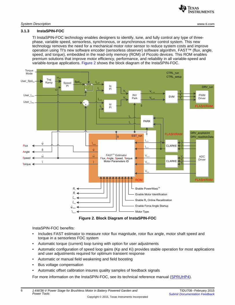
3.1.3 InstaSPIN-FOCTI InstaSPIN-FOC technology enables designers to identify, tune, and fully control any type of three-phase, variable speed, sensorless, synchronous, or asynchronous motor control system. This newtechnology removes the need for a mechanical motor rotor sensor to reduce system costs and improveoperation using TI's new software encoder (sensorless observer) software algorithm, FAST™ (flux, angle,speed, and torque), embedded in the read-only memory (ROM) of Piccolo devices. This ROM enablespremium solutions that improve motor efficiency, performance, and reliability in all variable-speed andvariable-torque applications. Figure 2 shows the block diagram of the InstaSPIN-FOC.
Figure 2. Block Diagram of InstaSPIN-FOC
InstaSPIN-FOC benefits:• Includes FAST estimator to measure rotor flux magnitude, rotor flux angle, motor shaft speed and
torque in a sensorless FOC system• Automatic torque (current) loop tuning with option for user adjustments• Automatic configuration of speed loop gains (Kp and Ki) provides stable operation for most applications
and user adjustments required for optimum transient response• Automatic or manual field weakening and field boosting• Bus voltage compensation• Automatic offset calibration insures quality samples of feedback signals
For more information on the InstaSPIN-FOC, see its technical reference manual (SPRUHP4).
6 1-kW/36-V Power Stage for Brushless Motor in Battery Powered Garden and TIDU708–February 2015Power Tools Submit Documentation Feedback
Copyright © 2015, Texas Instruments Incorporated
www.ti.com System Description
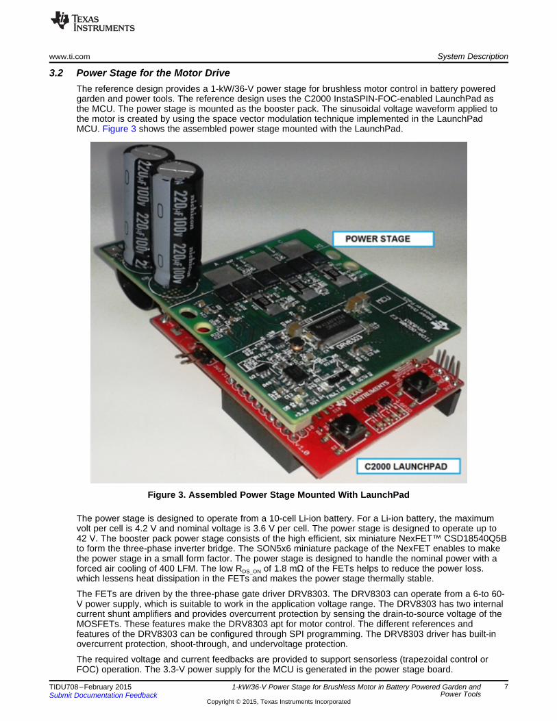
3.2 Power Stage for the Motor DriveThe reference design provides a 1-kW/36-V power stage for brushless motor control in battery poweredgarden and power tools. The reference design uses the C2000 InstaSPIN-FOC-enabled LaunchPad asthe MCU. The power stage is mounted as the booster pack. The sinusoidal voltage waveform applied tothe motor is created by using the space vector modulation technique implemented in the LaunchPadMCU. Figure 3 shows the assembled power stage mounted with the LaunchPad.
Figure 3. Assembled Power Stage Mounted With LaunchPad
The power stage is designed to operate from a 10-cell Li-ion battery. For a Li-ion battery, the maximumvolt per cell is 4.2 V and nominal voltage is 3.6 V per cell. The power stage is designed to operate up to42 V. The booster pack power stage consists of the high efficient, six miniature NexFET™ CSD18540Q5Bto form the three-phase inverter bridge. The SON5x6 miniature package of the NexFET enables to makethe power stage in a small form factor. The power stage is designed to handle the nominal power with aforced air cooling of 400 LFM. The low RDS_ON of 1.8 mΩ of the FETs helps to reduce the power loss.which lessens heat dissipation in the FETs and makes the power stage thermally stable.
The FETs are driven by the three-phase gate driver DRV8303. The DRV8303 can operate from a 6-to 60-V power supply, which is suitable to work in the application voltage range. The DRV8303 has two internalcurrent shunt amplifiers and provides overcurrent protection by sensing the drain-to-source voltage of theMOSFETs. These features make the DRV8303 apt for motor control. The different references andfeatures of the DRV8303 can be configured through SPI programming. The DRV8303 driver has built-inovercurrent protection, shoot-through, and undervoltage protection.
The required voltage and current feedbacks are provided to support sensorless (trapezoidal control orFOC) operation. The 3.3-V power supply for the MCU is generated in the power stage board.
7TIDU708–February 2015 1-kW/36-V Power Stage for Brushless Motor in Battery Powered Garden andPower ToolsSubmit Documentation Feedback
Copyright © 2015, Texas Instruments Incorporated
Brushless
motor
Offset
Offset
OPA2374
3.3 V
PWMs
DRV8303
36 VLi-ion
battery
pack
SPI
Three-
phase
NMOS
gate
driver
Control
and
protection
Temperature sensor output
TPS54061
Voltage
divider
LMT84
Motor voltage feedback
Motor current
feedback
CSD18540Q5B (x6)
Input DC voltage feedback
C2000 Insta
SP
IN-F
OC
LaunchP
ad Inte
rface
Shunt
Shunt
Shunt
TP
D45009
(TV
S)
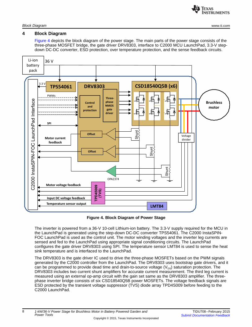
Block Diagram www.ti.com
4 Block DiagramFigure 4 depicts the block diagram of the power stage. The main parts of the power stage consists of thethree-phase MOSFET bridge, the gate driver DRV8303, interface to C2000 MCU LaunchPad, 3.3-V step-down DC-DC converter, ESD protection, over temperature protection, and the sense feedback circuits.
Figure 4. Block Diagram of Power Stage
The inverter is powered from a 36-V 10-cell Lithium-ion battery. The 3.3-V supply required for the MCU inthe LaunchPad is generated using the step-down DC-DC converter TPS54061. The C2000 InstaSPIN-FOC LaunchPad is used as the control unit. The motor winding voltages and the inverter leg currents aresensed and fed to the LaunchPad using appropriate signal conditioning circuits. The LaunchPadconfigures the gate driver DRV8303 using SPI. The temperature sensor LMT84 is used to sense the heatsink temperature and is interfaced to the LaunchPad.
The DRV8303 is the gate driver IC used to drive the three-phase MOSFETs based on the PWM signalsgenerated by the C2000 controller from the LaunchPad. The DRV8303 uses bootstrap gate drivers, and itcan be programmed to provide dead time and drain-to-source voltage (VDS) saturation protection. TheDRV8303 includes two current shunt amplifiers for accurate current measurement. The third leg current ismeasured using an external op-amp circuit with the gain set same as the DRV8303 amplifier. The three-phase inverter bridge consists of six CSD18540Q5B power MOSFETs. The voltage feedback signals areESD protected by the transient voltage suppressor (TVS) diode array TPD4S009 before feeding to theC2000 LaunchPad.
8 1-kW/36-V Power Stage for Brushless Motor in Battery Powered Garden and TIDU708–February 2015Power Tools Submit Documentation Feedback
Copyright © 2015, Texas Instruments Incorporated

www.ti.com Highlighted Products
5 Highlighted ProductsKey features of the highlighted devices are taken from product datasheets. The following are thehighlighted products used in this reference design.
5.1 DRV8303The DRV8303 is a gate driver IC for three-phase motor drive applications. The device provides three half-bridge drivers, each capable of driving two N-type MOSFETs (one for the high-side and one for the low-side). The DRV8303 supports up to a 2.3-A sink and a 1.7-A source peak current capability, and it onlyneeds a single power supply with a wide range from 6 to 60 V. The DRV8303 uses bootstrap gate driverswith trickle charge circuitry to support 100% duty cycle. The gate driver uses automatic hand shakingwhen high-side FET or low-side FET is switching to prevent current shoot through. The VDS of FETs issensed to protect external power stage during overcurrent conditions. The DRV8303 includes two currentshunt amplifiers for accurate current measurement. The current amplifiers support bi-directional currentsensing and provide an adjustable output offset of up to 3 V. The SPI provides detailed fault reporting andflexible parameter settings such as gain options for current shunt amplifier and slew rate control of thegate driver.
5.2 CSD18540Q5BThe CSD18540Q5B is a 60-V N-Channel NexFET Power MOSFET with a very low RDS_ON of 1.8 mΩ andfeatures very low total gate charge requirement. The CSD18540Q5B is available in very small package,SON 5×6 mm with a peak current rating of 400 A.
5.3 TPD4S009The TPD4S009 provide system level electrostatic discharge (ESD) solution for high-speed differentiallines. These devices offer four ESD clamp circuits for dual pair differential lines. The TPD4S009 offers anoptional VCC supply pin, which can be connected to system supply plane. A blocking diode at the VCC pinenables the Ioff feature for the TPD4S009. The TPD4S009 can handle live signal at the D+, D– pins whenthe VCC pin is connected to 0 V. The VCC pin allows all the internal circuit nodes of the TPD4S009 to be atknown potential during start up time. However, connecting the optional VCC pin to board supply plane doesnot affect the system level ESD performance of the TPD4S009. The TPD4S009 is offered in DBV, DCK,DGS, and DRY packages. The TPD4S009 comply with IEC 61000-4-2 (Level 4) ESD. The TPD4S009 ischaracterized for operation over the ambient air temperature range of –40°C to 85°C.
5.4 OPA2374The OPA2374 is a low-power and low-cost operational amplifier (op-amps) with excellent bandwidth (6.5MHz) and slew rate (5 V/μs). The input range extends 200 mV beyond the rails and the output range iswithin 25 mV of the rails. The speed-to-power ratio and small size make these op-amps ideal for portableand battery-powered applications. Under logic control, the amplifiers can be switched from normaloperation to a standby current that is less than 1 μA. These op-amps are specified for single or dualpower supplies of 2.7 to 5.5 V, with operation from 2.3 to 5.5 V. The OPA2374 can work in thetemperature range from −40°C to 125°C.
9TIDU708–February 2015 1-kW/36-V Power Stage for Brushless Motor in Battery Powered Garden andPower ToolsSubmit Documentation Feedback
Copyright © 2015, Texas Instruments Incorporated

Highlighted Products www.ti.com
5.5 TPS54061The TPS54061 device is a 60-V, 200-mA, synchronous step-down DC-DC converter with integrated high-side and low-side MOSFETs. Current mode control provides simple external compensation and flexiblecomponent selection. The non-switching supply current is 90 μA. Using the enable pin, shutdown supplycurrent is reduced to 1.4 μA. To increase light load efficiency, the low-side MOSFET emulates a diodewhen the inductor current reaches zero. Undervoltage lockout is internally set at 4.5 V but can beincreased using two resistors on the enable pin. The output voltage startup ramp is controlled by theinternal slow start time. The adjustable switching frequency range allows efficiency and externalcomponent size to be optimized. Frequency fold back and thermal shutdown protects the part during anoverload condition. The TPS54061 enables small designs by integrating the MOSFETs, boot rechargediode, and minimizing the IC footprint with a small 3×3-mm thermally enhanced VSON package.
5.6 LMT84The LMT84 is precision CMOS integrated-circuit temperature sensors with an analog output voltage that islinearly and inversely proportional to temperature. Its features make it suitable for many generaltemperature sensing applications. The LMT84 can operate down to a 1.5-V supply with a 5.4-μA powerconsumption, making the device ideal for battery-powered devices. Multiple package options, includingthrough-hole TO-92 and TO-126 packages, also allow the LMT84 to be mounted on board, off board, to aheat sink, or on multiple unique locations in the same application. Class-AB output structures gives theLMT84 strong output source and sink current capability that can directly drive up to 1.1-nF capacitiveloads. This capability means the device is well suited to drive an analog-to-digital converter sample-and-hold input with its transient load requirements. The LMT84 has accuracy capability specified in theoperating range of −50°C to 150°C. The accuracy, 3-lead package options, and other features also makethe LMT84 an alternative to thermistors.
10 1-kW/36-V Power Stage for Brushless Motor in Battery Powered Garden and TIDU708–February 2015Power Tools Submit Documentation Feedback
Copyright © 2015, Texas Instruments Incorporated
DC_V_FB
+PVDD
GNDGND
34.8kR20
0.1µFC23
3.3R21
0.01µFC24
0.1µFC22
DC_V_FB
2.20kR22
TP1
TP2
270µFC20
D3
1.5SMC56CA
PVDD
GND
270µFC21
( ) ( )max maxDC ADC _DC
2.20 k 34.8 k 2.20 k 34.8 kV V 3.3 55.5 V
2.20 k 2.20 k
W + W W + W= ´ = ´ =
W W
www.ti.com System Design Theory
6 System Design Theory
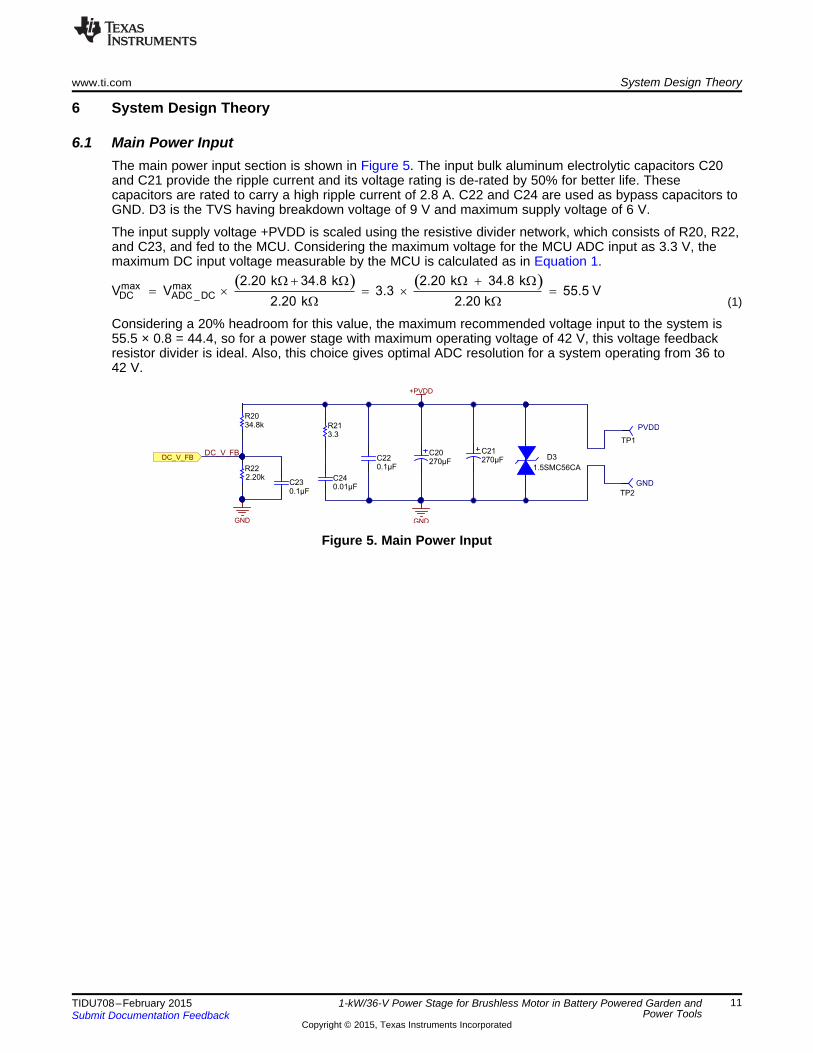
6.1 Main Power InputThe main power input section is shown in Figure 5. The input bulk aluminum electrolytic capacitors C20and C21 provide the ripple current and its voltage rating is de-rated by 50% for better life. Thesecapacitors are rated to carry a high ripple current of 2.8 A. C22 and C24 are used as bypass capacitors toGND. D3 is the TVS having breakdown voltage of 9 V and maximum supply voltage of 6 V.
The input supply voltage +PVDD is scaled using the resistive divider network, which consists of R20, R22,and C23, and fed to the MCU. Considering the maximum voltage for the MCU ADC input as 3.3 V, themaximum DC input voltage measurable by the MCU is calculated as in Equation 1.
(1)
Considering a 20% headroom for this value, the maximum recommended voltage input to the system is55.5 × 0.8 = 44.4, so for a power stage with maximum operating voltage of 42 V, this voltage feedbackresistor divider is ideal. Also, this choice gives optimal ADC resolution for a system operating from 36 to42 V.
Figure 5. Main Power Input
11TIDU708–February 2015 1-kW/36-V Power Stage for Brushless Motor in Battery Powered Garden andPower ToolsSubmit Documentation Feedback
Copyright © 2015, Texas Instruments Incorporated
+PVDD +PVDD +PVDD
GH_A
GL_A
GH_B
GL_B
GH_C
GL_C
SH_A
SH_BSH_C
SL_A
SL_BSL_C
A_ISENSE_N
A_ISENSE_PB_ISENSE_P
B_ISENSE_N
GND GND GND
C_ISENSE_P
C_ISENSE_N
2.2µFC28
2.2µFC29
2.2µFC30
1000pFC31
1000pFC32
1000pFC33
10
R28
10
R31
10
R29
10
R32
10
R30
10
R33
0.001R36
0.001R34
0.001R350
R52
0
R57
0
R54
0
R56
0
R53
0
R55
4
7,8
1,2
,3
5,6
,
Q3CSD18540Q5B
4
7,8
1,2
,3
5,6
,
Q8CSD18540Q5B
4
7,8
1,2
,3
5,6
, Q4CSD18540Q5B
4
7,8
1,2
,3
5,6
,
Q6CSD18540Q5B
4
7,8
1,2
,3
5,6
, Q7CSD18540Q5B
4
7,8
1,2
,3
5,6
,
Q5CSD18540Q5B
GND
C_ISENSE_N
C_ISENSE_P
B_ISENSE_N
B_ISENSE_PA_ISENSE_P
A_ISENSE_N
System Design Theory www.ti.com
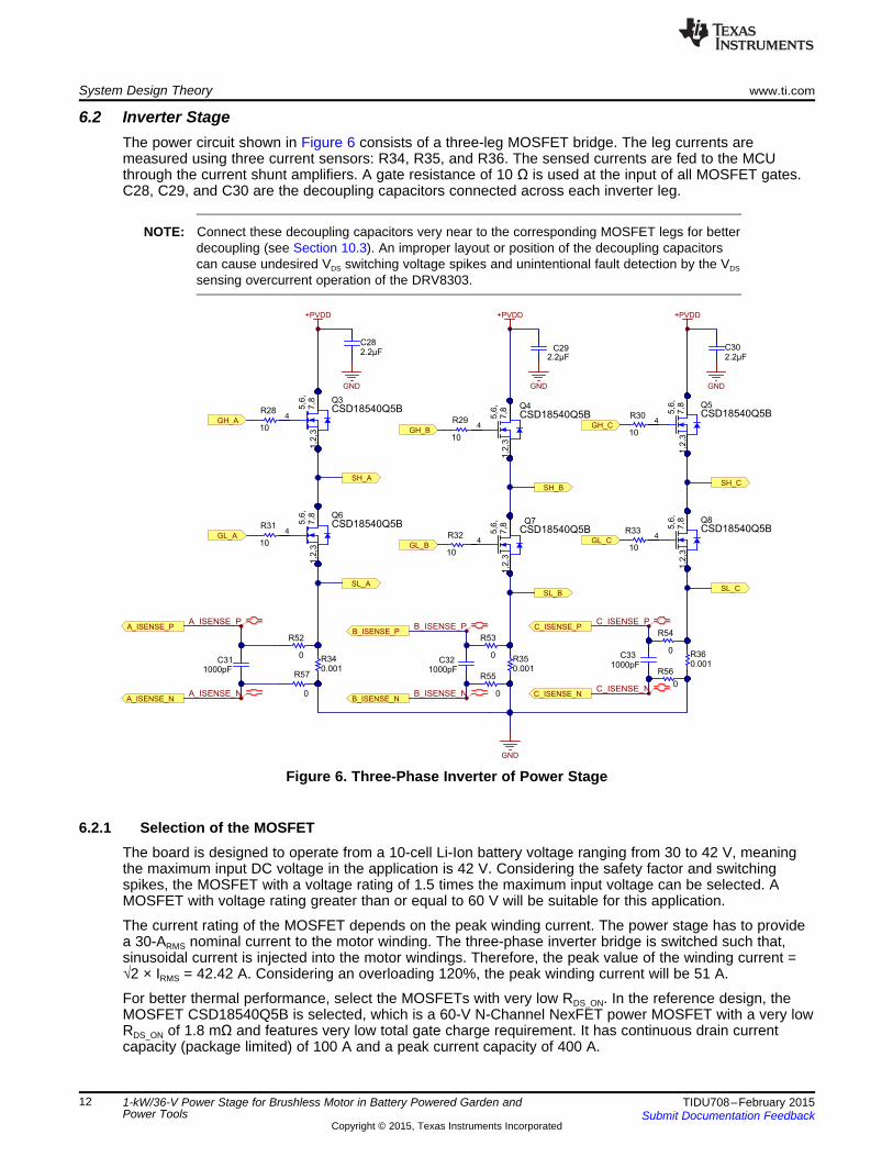
6.2 Inverter StageThe power circuit shown in Figure 6 consists of a three-leg MOSFET bridge. The leg currents aremeasured using three current sensors: R34, R35, and R36. The sensed currents are fed to the MCUthrough the current shunt amplifiers. A gate resistance of 10 Ω is used at the input of all MOSFET gates.C28, C29, and C30 are the decoupling capacitors connected across each inverter leg.
NOTE: Connect these decoupling capacitors very near to the corresponding MOSFET legs for betterdecoupling (see Section 10.3). An improper layout or position of the decoupling capacitorscan cause undesired VDS switching voltage spikes and unintentional fault detection by the VDS
sensing overcurrent operation of the DRV8303.
Figure 6. Three-Phase Inverter of Power Stage
6.2.1 Selection of the MOSFETThe board is designed to operate from a 10-cell Li-Ion battery voltage ranging from 30 to 42 V, meaningthe maximum input DC voltage in the application is 42 V. Considering the safety factor and switchingspikes, the MOSFET with a voltage rating of 1.5 times the maximum input voltage can be selected. AMOSFET with voltage rating greater than or equal to 60 V will be suitable for this application.
The current rating of the MOSFET depends on the peak winding current. The power stage has to providea 30-ARMS nominal current to the motor winding. The three-phase inverter bridge is switched such that,sinusoidal current is injected into the motor windings. Therefore, the peak value of the winding current =√2 × IRMS = 42.42 A. Considering an overloading 120%, the peak winding current will be 51 A.
For better thermal performance, select the MOSFETs with very low RDS_ON. In the reference design, theMOSFET CSD18540Q5B is selected, which is a 60-V N-Channel NexFET power MOSFET with a very lowRDS_ON of 1.8 mΩ and features very low total gate charge requirement. It has continuous drain currentcapacity (package limited) of 100 A and a peak current capacity of 400 A.
12 1-kW/36-V Power Stage for Brushless Motor in Battery Powered Garden and TIDU708–February 2015Power Tools Submit Documentation Feedback
Copyright © 2015, Texas Instruments Incorporated

2 2
RMS SENSEPower loss in the resistor I R 30 0.001 0.9 W= ´ = ´ =
www.ti.com System Design Theory
6.2.2 Selection of the Sense ResistorPower dissipation in sense resistors and the input offset error voltage of the op-amps are important inselecting the sense resistance values. The nominal RMS winding current in motor is 30 A. Therefore, thesense resistors will be carrying a nominal RMS current of 30 A with a peak value 30 × √2 = 42.42 A. Ahigh sense resistance value increases the power loss in the resistors. The internal current shunt amplifiersof the DRV8303 have a DC offset error of 4 mV. The DRV8303 can calibrate the DC offset. However, it isrequired to select the sense resistor such that the sense voltage across the resistor is sufficiently higherthan the offset error voltage to reduce the effect of the offset error.
Selecting a 1-mΩ resistor as the sense resistor, the power loss in the resistor at 30 ARMS is given byEquation 2:
(2)
Therefore, a standard 2-W, 2512-package resistor can be used. For the nominal 42.42 APEAK sinusoidalwinding current, the sense voltage have a peak value of 42.42 mV, which sufficiently larger than the offseterror of the op-amp.
13TIDU708–February 2015 1-kW/36-V Power Stage for Brushless Motor in Battery Powered Garden andPower ToolsSubmit Documentation Feedback
Copyright © 2015, Texas Instruments Incorporated
GND
OCTW
SCSVDD_SPI
EN_GATE
SDOSDO
SCS
GND
EN_GATE
FAULT
OCTW
GND
+3.3V+3.3V
+3.3V
VDD_SPI
1.0kR6
1.0R5
OCTW1
FAULT2
DTC3
SCS4
SDI5
SDO6
SCLK7
DC_CAL8
GVDD9
CP110
CP211
EN_GATE12
INH_A13
INL_A14
INH_B15
INL_B16
INH_C17
INL_C18
DVDD19
REF20
SO121
SO222
AVDD23
AGND24
PVDD25
SP226
SN227
SP128
SN129
SL_C30
GL_C31
SH_C32
GH_C33
BST_C34
SL_B35
GL_B36
SH_B37
GH_B38
BST_B39
SL_A40
GL_A41
SH_A42
GH_A43
BST_A44
VDD_SPI45
GND46
GND47
GND48
PAD49
U1
DRV8303DCA
SCLKSCLK
SDISDI
PWM_BH
PWM_BL
PWM_CH
PWM_CL
PWM_AH
PWM_AL
IA_FB
IB_FBIB_FB
IA_FB
1µFC16
GND
DVDD
1µFC17
GND
GND GND
B_ISENSE_N
B_ISENSE_P
DC_CALDC_CAL
GND
1.0kR9
+3.3V
A_ISENSE_P
A_ISENSE_N
SL_CSL_C
GL_CGL_C
GH_CGH_C
SH_CSH_C
0.1µFC7
GH_B
GL_B
SL_B
SH_B
GH_B
GL_B
SL_B
SH_B
0.1µFC6
GH_A
GL_A
SL_A
SH_A
GH_A
GL_A
SL_A
SH_A
0.1µFC5 GND
2.2µFC40.022µF
C3
+PVDD
GND
0.1µFC2
2.2µFC1
C1
A2
RED
D2
D-LED_0805
G1
S2
D3
P_CHQ2
GND
330R4
C1
A2
YELLOW
D1
D-LED_0805
GND
330R1
G1
S2
D3
P_CHQ1
+3.3V
+3.3V
GND
VDD_SPI
0R14
0.1µF, DNP
C19
FAULT
2.2µF
C39
2.2µFC15
3.3kR2
3.3kR3
A_ISENSE_PA_ISENSE_N
B_ISENSE_PB_ISENSE_N
System Design Theory www.ti.com
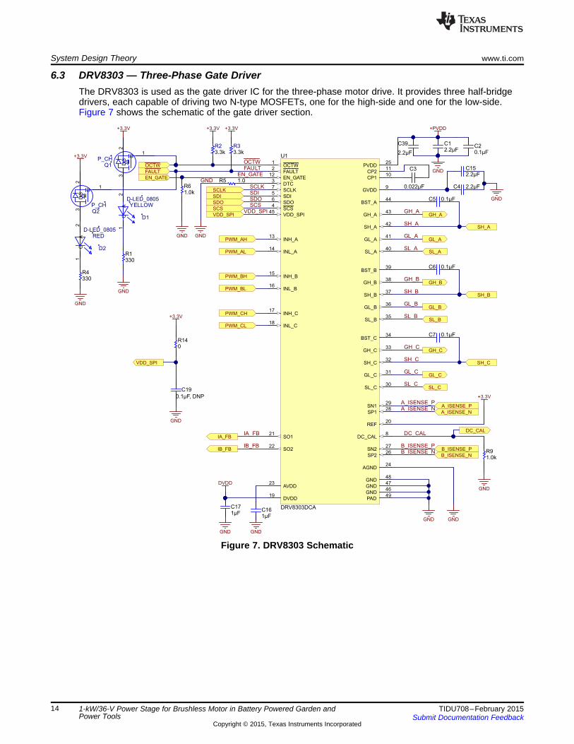
6.3 DRV8303 — Three-Phase Gate DriverThe DRV8303 is used as the gate driver IC for the three-phase motor drive. It provides three half-bridgedrivers, each capable of driving two N-type MOSFETs, one for the high-side and one for the low-side.Figure 7 shows the schematic of the gate driver section.
Figure 7. DRV8303 Schematic
14 1-kW/36-V Power Stage for Brushless Motor in Battery Powered Garden and TIDU708–February 2015Power Tools Submit Documentation Feedback
Copyright © 2015, Texas Instruments Incorporated

www.ti.com System Design Theory
The gate driver has following features:• Internal handshake between high-side and low-side FETs during switching transition to prevent current
shoot through• Programmable slew rate or current driving capability through SPI• Supports up to 200-kHz switching frequency with Qg(TOT) = 25 nC or total 30-mA gate drive average
current• Provide cycle-by-cycle (CBC) current limiting and latch overcurrent shut down of external FETs.
Current is sensed through FET VDS and the overcurrent level is programmable through SPI. VDSsensing range is programmable from 0.060 to 2.4 V with 5-bit resolution
• High-side gate drive will survive negative output from half bridge up to –10 V for 10 ns• During EN_GATE pin low and fault conditions, the gate driver keeps external FETs in high impedance
mode• Programmable dead time through DTC pin. Dead time control range: 50 to 500 ns. Shorting DTC pin to
ground will provide minimum dead time of 50 ns. External dead time will override internal dead time aslong as the time is longer than the dead time setting
• Bootstraps circuits are used to drive high-side FETs of three-phase inverter. Trickle charge circuitry isused to replenish current leakage from bootstrap cap and support 100% duty cycle operation
In Figure 7, C1, C2, and C39 are the PVDD decoupling capacitors. PVDD decoupling capacitors shouldbe placed close to their corresponding pins with a low impedance path to device GND (PowerPAD) (SeeSection 10.3 for more details). PVDD is the power supply pin for gate driver. The DRV8303 providespower stage undervoltage protection by driving its outputs low whenever PVDD is below 6 V (PVDD_UV).The PVDD undervoltage will be reported through FAULT pin and SPI status register. C5, C6, and C7 arethe bootstrap capacitors. The detailed design and features of the DRV8303 are explained in the followingsections.
6.3.1 Internal Regulator Voltages of DRV8303AVDDAVDD is the internal 6-V supply voltage. Connect the AVDD capacitor to the AGND. AVDD is an output,but not specified to drive external circuitry. In the schematic, C16 is used as the AVDD capacitor with arecommended value of 1 uF. Typical AVDD voltage is 6.5 V. The minimum specified value is 6 V and amaximum of 7 V.
DVDDInternal 3.3-V supply voltage. Connect the DVDD capacitor to the AGND. DVDD is an output, but notspecified to drive external circuitry. In the schematic, C17 is used as the DVDD capacitor with arecommended value of 1 uF. Place AVDD and DVDD capacitors close to their corresponding pins with alow impedance path to the AGND pin (see Section 10.3 for more details). Make this connection on thesame layer. Tie AGND to device GND (PowerPAD) through a low-impedance trace or copper fill. TypicalDVDD voltage is 3.3 V. The minimum specified value is 3 V and maximum is 3.6 V. If DVDD goes toundervoltage, the external FETs go to high-impedance state by means of weak pull down of all gate driveroutput. On recovering from undervoltage, the DRV8303 resets the SPI registers. The DVDD undervoltagewill be reported through FAULT pin.
GVDDGVDD is the voltage output from internal gate driver voltage regulator. The capacitor C15 is connected tothe GVDD pin. Connect the GVDD capacitor to GND. Typically, use a 2.2-uF ceramic capacitor as theGVDD capacitor. Place the GVDD capacitor close to its corresponding pin with a low-impedance path todevice GND (PowerPAD) (See Section 10.3 for more details). GVDD pin is protected from undervoltageand overvoltage. The undervoltage protection limit is 7.5 V and overvoltage protection limit is 16 V. Whenundervoltage protection is triggered, the DRV8303 outputs are driven low and the external MOSFETs willgo to a high-impedance state. The GVDD undervoltage will be reported through FAULT pin and SPI statusregister. The GVDD overvoltage fault is a latched fault and can only be reset through a transition onEN_GATE pin. The GVDD overvoltage will be reported through FAULT pin and SPI status register.
15TIDU708–February 2015 1-kW/36-V Power Stage for Brushless Motor in Battery Powered Garden andPower ToolsSubmit Documentation Feedback
Copyright © 2015, Texas Instruments Incorporated
SN
SP
SO
_
+
DC_CAL
DC_CAL
DC_CAL
S1
S2
S4
S3
S1
S2
S4
S3
5kW
5kW
400kW
200kW
100kW
50kW
400kW
200kW
100kW
50kW
100W
_
+
REF
Vref/2
AVDD
AVDD
50kW
50kW
( )ref
O X X
VV G SN SP
2= - ´ -
System Design Theory www.ti.com
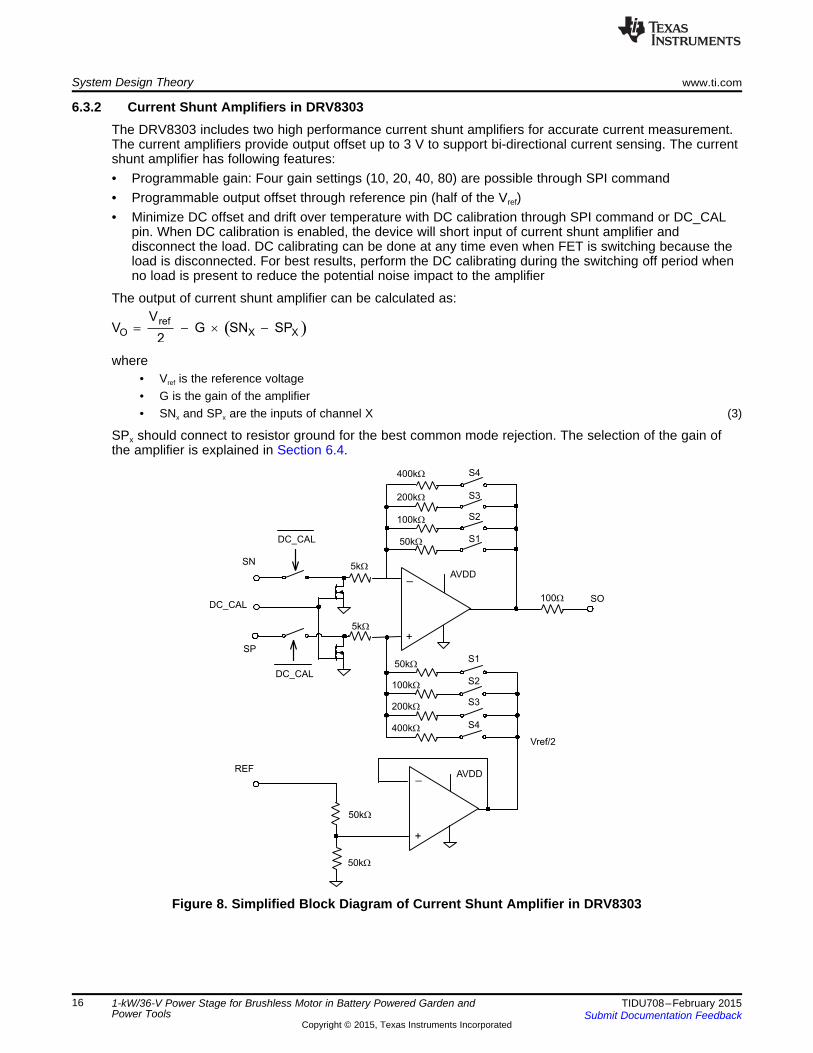
6.3.2 Current Shunt Amplifiers in DRV8303The DRV8303 includes two high performance current shunt amplifiers for accurate current measurement.The current amplifiers provide output offset up to 3 V to support bi-directional current sensing. The currentshunt amplifier has following features:• Programmable gain: Four gain settings (10, 20, 40, 80) are possible through SPI command• Programmable output offset through reference pin (half of the Vref)• Minimize DC offset and drift over temperature with DC calibration through SPI command or DC_CAL
pin. When DC calibration is enabled, the device will short input of current shunt amplifier anddisconnect the load. DC calibrating can be done at any time even when FET is switching because theload is disconnected. For best results, perform the DC calibrating during the switching off period whenno load is present to reduce the potential noise impact to the amplifier
The output of current shunt amplifier can be calculated as:
where• Vref is the reference voltage• G is the gain of the amplifier• SNx and SPx are the inputs of channel X (3)
SPx should connect to resistor ground for the best common mode rejection. The selection of the gain ofthe amplifier is explained in Section 6.4.
Figure 8. Simplified Block Diagram of Current Shunt Amplifier in DRV8303
16 1-kW/36-V Power Stage for Brushless Motor in Battery Powered Garden and TIDU708–February 2015Power Tools Submit Documentation Feedback
Copyright © 2015, Texas Instruments Incorporated
www.ti.com System Design Theory
6.3.3 Protection Features in DRV8303Overcurrent Protection and ReportingTo protect the power stage from damage due to high currents, a VDS sensing circuitry is implemented inthe DRV8303. Based on the RDS_ON of the power MOSFETs and the maximum allowed drain current, avoltage threshold can be calculated which, when exceeded, triggers the overcurrent protection feature.This voltage threshold level is programmable through SPI command.
There are total four OC_MODE settings in SPI:1. Current limit mode
When current limit mode is enabled, the DRV8303 limits the MOSFET current instead of shutting downduring the overcurrent event. The overcurrent event is reported through the overcurrent temperaturewarning (OCTW) pin. OCTW reporting will hold low during same PWM cycle or for a max 64-μs period(internal timer) so that the external controller has enough time to sample the warning signal. If in themiddle of reporting other FETs get overcurrent, then OCTW reporting will hold low and recount another64 μs unless PWM cycles on both FETs are ended.There are two current control settings in current limit mode (selected by one bit in SPI and default isCBC mode):• Setting 1 (CBC mode): during overcurrent event, the FET that detected overcurrent will turn off until
next PWM cycle.• Setting 2 (off-time control mode):
– During overcurrent event, the FET that detected overcurrent will turn off for 64 µs as off timeand back to normal after that (so same FET will be on again) if PWM signal is still holding high.Since all three phases or six FETs share a single timer, if more than one FET get overcurrent,the FETs will not be back to normal until the all FETs that have overcurrent event pass 64 μs.
– If PWM signal is toggled for this FET during timer running period, device will resume normaloperation for this toggled FET. So real off-time could be less than 64 µs in this case.
– If two FETs get overcurrent and one FET’s PWM signal gets toggled during timer runningperiod, this FET will be back to normal, and the other FET will be off until the timer ends (unlessits PWM is also toggled).
2. Overcurrent latch shutdown modeWhen overcurrent occurs, the device will turn off both high-side and low-side FETs in the same phaseif any of the FETs in that phase have overcurrent.
3. Report only modeNo protection action will be performed in this mode. Overcurrent detection will be reported through theOCTW pin and SPI status register. External MCU takes actions based on its own control algorithm. Apulse stretching of 64 μs will be implemented on OCTW pin so the controller can have enough time tosense the overcurrent signal.
4. Overcurrent disable modeThe device will ignore all the overcurrent detections and will not report them either.
Undervoltage ProtectionTo protect the power stage during undervoltage conditions, the DRV8303 provides power stageundervoltage protection by driving its outputs low whenever PVDD is below 6 V (PVDD_UV) or GVDD isbelow 7.5 V (GVDD_UV). When undervoltage protection is triggered, the DRV8303 outputs are driven lowand the external MOSFETs will go to a high impedance state.
Overvoltage Protection (GVDD_OV)The DRV8303 will shut down both the gate driver and charge pump if GVDD voltage exceeds 16 V toprevent potential issue related to the GVDD or charge pump (for example, short of external GVDD cap orcharge pump). The fault is a latched fault and can only be reset through a transition on EN_GATE pin.
17TIDU708–February 2015 1-kW/36-V Power Stage for Brushless Motor in Battery Powered Garden andPower ToolsSubmit Documentation Feedback
Copyright © 2015, Texas Instruments Incorporated

System Design Theory www.ti.com
Over Temperature ProtectionA two-level over temperature detection circuit is implemented in the DRV8303:• Level 1: over temperature warning (OTW). OTW is reported through OCTW pin for default setting. The
OCTW pin can be set to report OTW or overcurrent warning only through SPI command.• Level 2: over temperature latched shut down of gate driver and charge pump (OTSD_GATE). The fault
will be reported to the FAULT pin. This pin is a latched shut down, so the gate driver will not berecovered automatically—even over temperature condition is not present anymore. An EN_GATE resetthrough pin or SPI (RESET_GATE) is required to recover gate driver to normal operation aftertemperature goes below a preset value, tOTSD_CLR. SPI operation is still available and register settingswill be remaining in the device during OTSD operation as long as PVDD is still within defined operationrange.
Junction temperature for resetting over temperature warning (OTW_CLR) is 115°C. Junction temperaturefor the over temperature warning and resetting over temperature shutdown (OTW_SET/OTSD_CLR) is130°C.
Fault and Protection HandlingThe FAULT pin indicates an error event (with shutdown) has occurred such as overcurrent, overtemperature, overvoltage, or undervoltage. Note that FAULT is an open-drain signal. FAULT will go highwhen gate driver is ready for PWM signal (internal EN_GATE goes high) during start up. The OCTW pinindicates overcurrent event and over temperature event that not necessary related to shut down. OCTW isan open-drain signal.
EN_GATEEN_GATE low is used to put the gate driver, charge pump, current shunt amplifier, and internal regulatorblocks into a low-power consumption mode to save energy. SPI communication is not supported duringthis state. The device will put the MOSFET output stage to a high-impedance mode as long as PVDD isstill present. When EN_GATE pin goes high, it will go through a power-up sequence, and enable gatedriver, current amplifiers, charge pump, internal regulator, and so on and reset all latched faults related tothe gate driver block. The pin will also reset status registers in the SPI table. All latched faults can be resetwhen EN_GATE is toggled after an error event unless the fault is still present. When EN_GATE goes fromhigh to low, it will shut down gate driver block immediately, so the gate output can put external FETs inhigh impedance mode. It will then wait for 10 µs before completely shutting down the rest of the blocks.
A quick fault reset mode can be done by toggling EN_GATE pin for a very short period (less than 10 μs).This will prevent device to shut down other function blocks such as charge pump and internal regulatorsand bring a quicker and simple fault recovery. SPI will still function with such a quick EN_GATE resetmode. The other way to reset all the faults is to use SPI command (RESET_GATE), which will only resetgate driver block and all the SPI status registers without shutting down other function blocks. Oneexception is to reset a GVDD_OV fault. A quick EN_GATE quick fault reset or SPI command reset will notwork with GVDD_OV fault. A complete EN_GATE with low level holding longer than 10 μs is required toreset GVDD_OV fault. Inspect the system and board when GVDD_OV occurs.
DTCDead time can be programmed through DTC pin. Connect a resistor from DTC to ground to control thedead time. Dead time control range is from 50 to 500 ns. A short DTC pin to ground will provide theminimum dead time (50 ns). The resistor range is 0 to 150 kΩ. Dead time is linearly set over this resistorrange. Current shoot through prevention protection is constantly enabled in the device, independent ofdead time setting and input mode setting. In the reference design, a 1-Ω resistor is connected to the DTCpin.
18 1-kW/36-V Power Stage for Brushless Motor in Battery Powered Garden and TIDU708–February 2015Power Tools Submit Documentation Feedback
Copyright © 2015, Texas Instruments Incorporated

www.ti.com System Design Theory
6.3.4 SPI CommunicationVDD_SPIVDD_SPI is the power supply to power SDO pin. It has to be connected to the same power supply (3.3 Vor 5 V) that the MCU uses for its SPI operation. During power up or down transient, VDD_SPI pin couldbe zero voltage shortly. During this period, no SDO signal should be present at the SDO pin from anyother devices in the system because it causes a parasitic diode in the DRV8303 conducting from SDO toVDD_SPI pin as a short. This should be considered and prevented from system power sequence design.
DC_CALWhen DC_CAL is enabled, the device will short inputs of the shunt amplifier and disconnect from the load,so the external microcontroller (or SPI command) can calibrate the DC offset. Using the SPI exclusivelyfor DC calibration, the DC_CAL pin can be connected to GND.
SPI PinsThe SDO pin has to be 3-state, so a data bus line can be connected to multiple SPI slave devices. TheSCS pin is active low. When SCS is high, SDO is at high impendence mode.
SPISPI is used to set device configuration, operating parameters and read out diagnostic information. TheDRV8303 SPI operates in the slave mode. The SPI input data (SDI) word consists of 16-bit word, with 11-bit data and 5-bit (MSB) command. The SPI output data (SDO) word consists of 16-bit word, with 11-bitregister data and 4-bit MSB address data and one frame fault bit (active 1). When a frame is not valid,frame fault bit will set to 1, and rest of SDO bit will shift out zeroes.
A valid frame has to meet following conditions:1. Clock must be low when /SCS goes low.2. Clock must have 16 full cycles.3. Clock must be low when /SCS goes high.
When SCS is asserted high, any signals at the SCLK and SDI pins are ignored, and SDO is forced into ahigh impedance state. When SCS transitions from high to low, SDO is enabled and the SPI responseword loads into the shift register based on 5-bit command in SPI at the previous clock cycle. The SCLKpin must be low when SCS transitions low. While SCS is low, at each rising edge of the clock, theresponse bit is serially shifted out on the SDO pin with MSB shifted out first. While SCS is low, at eachfalling edge of the clock, the new control bit is sampled on the SDI pin. The SPI command bits aredecoded to determine the register address and access type (read or write). The MSB will be shifted infirst. If the word sent to SDI is less than 16 bits or more than 16 bits, it is considered a frame error. If it is awrite command, the data will be ignored. The fault bit in SDO (MSB) will report 1 at next 16-bit word cycle.After the 16th clock cycle or when SCS transitions from low to high, in case of write access type, the SPIreceive shift register data is transferred into the latch where address matches decoded SPI commandaddress value. Any amount of time may pass between bits as long as SCS stays active low, which allowstwo 8-bit words to be used.
For a read command (Nth cycle) in SPI, SPO will send out data in the register with address in readcommand in next cycle (N+1). For a write command in SPI, SPO will send out data in the status register0x00h in next 16-bit word cycle (N+1). For most of the time, this feature will maximize SPI communicationefficiency when having a write command, but still get fault status values back without sending extra readcommand.
SPI FormatAn SPI input data control word is 16 bits long, consisting of:• 1 read or write bit W [15]• 4 address bits A [14:11]• 11 data bits D [10:0]
An SPI output data response word is 16 bits long, and its content depends on the given SPI command(SPI Control Word) in the previous cycle. When an SPI Control Word is shifted in, the SPI Response Word(that is shifted out during the same transition time) is the response to the previous SPI Command (shift inSPI Control Word 'N' and shift out SPI Response Word "N-1"). Therefore, each SPI Control / Responsepair requires two full 16-bit shift cycles to complete. The definitions of all SPI registers are given in thedatasheet of DRV8303 (SLOS846).
19TIDU708–February 2015 1-kW/36-V Power Stage for Brushless Motor in Battery Powered Garden andPower ToolsSubmit Documentation Feedback
Copyright © 2015, Texas Instruments Incorporated
GND
+3.3V
GND
IC_FB
C_ISENSE_P
C_ISENSE_N
10.0kR48
10.0kR46
+3.3V
GND
2.2µFC38
0.1µFC37
1.00kR44
1.00kR45
0.1µF
C13
GND
100
R50
1
3
24
8U3A
OPA2374AID
7
5
6
48
U3B
OPA2374AID
20.0k
R43
20.0k
R47
C_ISENSE_P
C_ISENSE_N
System Design Theory www.ti.com
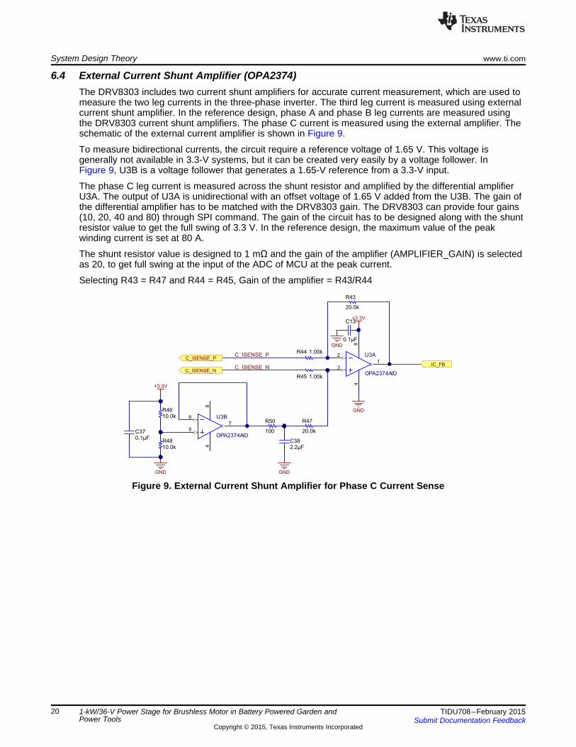
6.4 External Current Shunt Amplifier (OPA2374)The DRV8303 includes two current shunt amplifiers for accurate current measurement, which are used tomeasure the two leg currents in the three-phase inverter. The third leg current is measured using externalcurrent shunt amplifier. In the reference design, phase A and phase B leg currents are measured usingthe DRV8303 current shunt amplifiers. The phase C current is measured using the external amplifier. Theschematic of the external current amplifier is shown in Figure 9.
To measure bidirectional currents, the circuit require a reference voltage of 1.65 V. This voltage isgenerally not available in 3.3-V systems, but it can be created very easily by a voltage follower. InFigure 9, U3B is a voltage follower that generates a 1.65-V reference from a 3.3-V input.
The phase C leg current is measured across the shunt resistor and amplified by the differential amplifierU3A. The output of U3A is unidirectional with an offset voltage of 1.65 V added from the U3B. The gain ofthe differential amplifier has to be matched with the DRV8303 gain. The DRV8303 can provide four gains(10, 20, 40 and 80) through SPI command. The gain of the circuit has to be designed along with the shuntresistor value to get the full swing of 3.3 V. In the reference design, the maximum value of the peakwinding current is set at 80 A.
The shunt resistor value is designed to 1 mΩ and the gain of the amplifier (AMPLIFIER_GAIN) is selectedas 20, to get full swing at the input of the ADC of MCU at the peak current.
Selecting R43 = R47 and R44 = R45, Gain of the amplifier = R43/R44
Figure 9. External Current Shunt Amplifier for Phase C Current Sense
20 1-kW/36-V Power Stage for Brushless Motor in Battery Powered Garden and TIDU708–February 2015Power Tools Submit Documentation Feedback
Copyright © 2015, Texas Instruments Incorporated

( ) ( )Ia
maxADCmax
aSENSE
V 1.65 3.3 1.65I 82.5
R AMPLIFIER _ GAIN 0.001 20
- -= = =
´ ´
max maxa SENSE ADC _Ia1.65 (I R AMPLIFIER _ GAIN) V+ ´ ´ =
( )SENSECOutput of the current shunt amplifier 1.65 I R AMPLIFIER _ GAIN= + ´ ´
www.ti.com System Design Theory
6.5 Motor Current Sensing — SettingsThe motor current sensing amplifier gain has to be designed to get maximum resolution from the ADC ofthe MCU. Considering the external shunt amplifier, the output of the current shunt amplifier can be writtenas in Equation 4:
(4)
Here, IC is the phase C leg current. Equation 4 is also valid for the current shunt amplifiers in theDRV8303 used for phase A and phase B leg current sensing. The maximum leg current feedbackmeasurable by the MCU can be calculated as follows, considering the maximum voltage for the ADC inputis 3.3 V:
If Iamax is the peak value of the phase A leg current measurable by the ADC, then
(5)
(6)
Therefore, the peak-to-peak maximum current measurable by the ADC is 165 A. With this currentfeedback circuit, the following setting is done in user.h (see Section 7 for the details about user.h).
NOTE: USER_IQ_FULL_SCALE_CURRENT_A is a parameter used in user.h, which defines the fullscale current for the IQ variables. This value must be larger than the maximum currentreadings that you are expecting from the motor. If the measured current is greater than theUSER_IQ_FULL_SCALE_CURRENT_A at any point, there might be a numerical overflowcondition in the software. Make sure the measurable current is less than this value to avoidan undesirable software behavior.
To avoid this issue, make sure that (USER_IQ_FULL_SCALE_CURRENT_A × 2) is alwaysgreater than the measurable current by the ADC. The "multiply by 2" factor is because theUSER_IQ_FULL_SCALE_CURRENT_A parameter ranges from zero to maximum amplitude(peak), while the USER_ADC_FULL_SCALE_ CURRENT_A is from peak to peak.
See the INSTA-FOC user's guide for more details (SPRUHJ1).
21TIDU708–February 2015 1-kW/36-V Power Stage for Brushless Motor in Battery Powered Garden andPower ToolsSubmit Documentation Feedback
Copyright © 2015, Texas Instruments Incorporated
( ) ( )max maxa ADC _ a
2.20 k 34.8 k 2.20 k 34.8 kV V 3.3 55.5 V
2.20 k 2.20 k
W + W W + W= ´ = ´ =
W W
SH_A VA_FB
SH_B VB_FB
SH_C VC_FB
GND GND
GND GND
GND GND
VC_FB
VB_FB
VA_FB
34.8k
R37
34.8k
R39
34.8k
R41
0.1µFC34
0.1µFC35
0.1µFC36
2.20kR38
2.20kR40
2.20kR42
System Design Theory www.ti.com
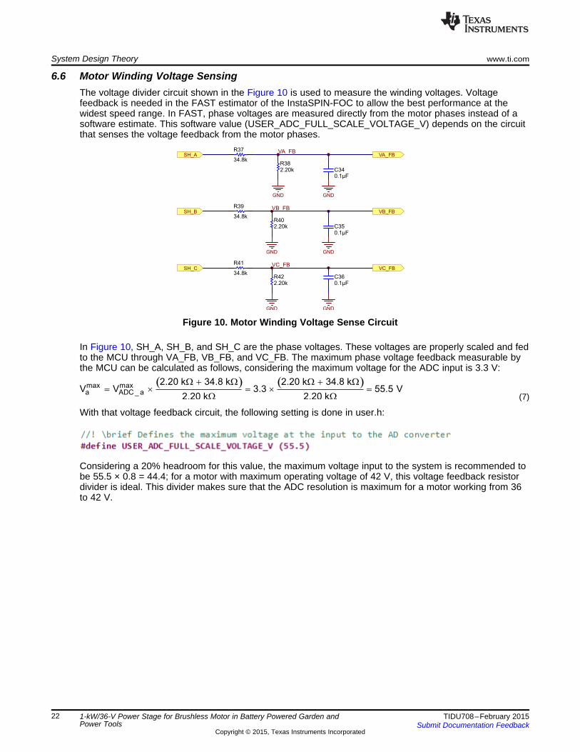
6.6 Motor Winding Voltage SensingThe voltage divider circuit shown in the Figure 10 is used to measure the winding voltages. Voltagefeedback is needed in the FAST estimator of the InstaSPIN-FOC to allow the best performance at thewidest speed range. In FAST, phase voltages are measured directly from the motor phases instead of asoftware estimate. This software value (USER_ADC_FULL_SCALE_VOLTAGE_V) depends on the circuitthat senses the voltage feedback from the motor phases.
Figure 10. Motor Winding Voltage Sense Circuit
In Figure 10, SH_A, SH_B, and SH_C are the phase voltages. These voltages are properly scaled and fedto the MCU through VA_FB, VB_FB, and VC_FB. The maximum phase voltage feedback measurable bythe MCU can be calculated as follows, considering the maximum voltage for the ADC input is 3.3 V:
(7)
With that voltage feedback circuit, the following setting is done in user.h:
Considering a 20% headroom for this value, the maximum voltage input to the system is recommended tobe 55.5 × 0.8 = 44.4; for a motor with maximum operating voltage of 42 V, this voltage feedback resistordivider is ideal. This divider makes sure that the ADC resolution is maximum for a motor working from 36to 42 V.
22 1-kW/36-V Power Stage for Brushless Motor in Battery Powered Garden and TIDU708–February 2015Power Tools Submit Documentation Feedback
Copyright © 2015, Texas Instruments Incorporated

filter _ poleparallel
1 1F 769.16 Hz
2 R C 34.8 k 2.2 k2 0.1 F
34.8 k 2.2 k
= = =´ p ´ ´ æ öW ´ W
´ p ´ ´ mç ÷W + Wè ø
www.ti.com System Design Theory
The voltage filter pole is needed by the FAST estimator to allow an accurate detection of the voltagefeedback. The filter cut off frequency should be low enough to filter out the PWM signals. As a generalguideline, a cutoff frequency of a few hundred Hertz is enough to filter out a PWM frequency of 10 to 20kHz. The hardware filter should only be changed when ultra-high speed motors are run, which generatephase voltage frequencies of a few kHz. In this reference design, consider the PMSM with a maximumspeed of about 3,000 RPM with eight pole pairs. This motor gives a voltage frequency of 3000 × 8 / 60 =400 Hz. The voltage filter of around this frequency of 400 Hz should be enough cutoff frequency for thismotor and speed. The filter pole setting can be calculated as follows:
(8)
The following code example shows how this is defined in user.h:
NOTE: The parameter USER_IQ_FULL_SCALE_VOLTAGE_V defines the full-scale value for theIQ30 variable of voltage inside the system. All voltages are converted into per unit based onthe ratio to this value. This value must be larger than the maximum value of any voltagecalculated inside the control system otherwise the value can saturate and roll over, causingan inaccurate value. This value is often greater than the maximum measured ADC value,especially with high BEMF motors operating at higher than rated speeds. If the value of yourBEMF constant is known and the design is operating at a speed higher than its rated speeddue to field weakening, set this value higher than the expected BEMF voltage.
See the InstaSPIN-FOC user's guide for more details (SPRUHJ1).
23TIDU708–February 2015 1-kW/36-V Power Stage for Brushless Motor in Battery Powered Garden andPower ToolsSubmit Documentation Feedback
Copyright © 2015, Texas Instruments Incorporated

BOOT1
VIN2
EN3
RT/CLK4
VSNS5
COMP6
GND7
PH8
PW
PD
9
U4
TPS54061DRB
2.2µFC9
22µFC10
97.6kR49
38.3kR11
0.012µF
C1233pFC11
30.9kR7
10.0kR12
120µH
L1+PVDD
+3.3V
GND
0.01µF
C8
909kR8
34.8kR10
System Design Theory www.ti.com
6.7 Design of 36-V to 3.3-V Step-Down DC-DC ConverterThe 3.3-V regulated power supply for the board is derived using the switching converter TPS54061. TheTPS54061 device is a 60-V, 200-mA, step-down (buck) regulator with an integrated high-side and low-siden-channel MOSFET. To improve performance during line and load transients, the device implements aconstant frequency, current mode control, which reduces output capacitance and simplifies externalfrequency compensation design. The design specifications of the step-down converter are given inTable 2. The schematic of the step-down converter is shown in Figure 11.
Table 2. Design Specifications of Step-Down Converter
PARAMETER VALUEConduction mode Continuous conduction mode (CCM)
Output voltage 3.3 VMaximum output current 150 mA
Input voltage 36 V nominal (36 to 42 V)Output voltage ripple 0.5% of VOUT
Start input voltage (rising VIN) 33 VStop input voltage (falling VIN) 30 V
Figure 11. 36-V to 3.3-V Step-Down Converter
The following parameters symbols are used for the further analysis of the buck converter:• LO,min — Minimum value of output inductor• LO — Output inductor• VIN,max — Maximum value of input voltage• VIN,min — Minimum value of input voltage• VOUT — Output voltage• IOUT — Average output current• fsw — Switching frequency
24 1-kW/36-V Power Stage for Brushless Motor in Battery Powered Garden and TIDU708–February 2015Power Tools Submit Documentation Feedback
Copyright © 2015, Texas Instruments Incorporated

RIPPLE
out
RIPPLE sw
I 1C
V 8 f
æ ö³ ´ ç ÷
ç ÷´è ø
RIPPLEL OUT
I 0.04422I peak I 0.15 0.172 A
2 2= + = + =
( )
( )
2
OUT IN OUT2
L O
IN O sw
2
2
L 6 3
V V max V1I rms I
12 V max L f
3.3 42 3.31I rms 0.15 0.15 A
12 42 120 10 573 10-
æ ö´ -= + ´ ç ÷
ç ÷´ ´è ø
æ ö´ -= + ´ =ç ÷ç ÷´ ´ ´ ´è ø
( ) ( )OUT IN OUT
RIPPLE 6 3IN O sw
V V max V 3.3 42 3.3I 44.22 mA
V max L f 42 120 10 573 10-
´ - ´ -³ = =
´ ´ ´ ´ ´ ´
IN,max OUT OUTO,min 3
IND O IN,max sw
V V V 42 3.3 3.3L 89 H
K I V f 0.4 0.15 42 573 10
- -³ ´ = ´ = m
´ ´ ´ ´ ´
( )( )
T 1.039
sw
71657R k
f kHz
W =
www.ti.com System Design Theory
6.7.1 Selecting the Switching FrequencyThe switching frequency of the TPS54061 is adjustable over a wide range, from 50 kHz to 1100 kHz, byvarying the resistor on the RT/CLK pin. The RT/CLK pin voltage is typically 0.53 V and must have aresistor to ground to set the switching frequency. To reduce the solution size, set the switching frequencyas high as possible; however, consider the tradeoffs of the supply efficiency, maximum input voltage, andminimum controllable on time. The minimum controllable on time is typically 120 ns and limits theoperating frequency for high input voltages. To determine the timing resistance (RT) for a given switchingfrequency, use Equation 9.
(9)
The switching frequency is set by resistor R49 shown in Figure 11. The reference design uses a switchingfrequency of 573 kHz.
6.7.2 Output Inductor Selection (LO)To calculate the minimum value of the output inductor, use Equation 10:
(10)
KIND is a coefficient that represents the amount of inductor ripple current relative to the maximum outputcurrent. This design uses a KIND of 0.4. The minimum inductor value is calculated to be greater than 89μH. For this design, a standard 120-μH value was chosen as the LO. The inductor current ripple (IRIPPLE),RMS inductor current (ILrms), and peak inductor current (ILpeak) can be calculated using Equation 11through Equation 13.
(11)
(12)
(13)
For this design, the RMS inductor current is 150 mA and the peak inductor current is 172 mA. The choseninductor has a saturation current rating of 250 mA and an RMS current rating of 220 mA. In transientconditions, the inductor current can increase up to the switch current limit of the device. For this reason,the most conservative approach is to specify an inductor with a saturation current rating equal to orgreater than the switch current limit rather than the calculated peak inductor current.
6.7.3 Output CapacitorConsider these three aspects when selecting the value of the output capacitor: the modulator pole, theoutput voltage ripple, and how the regulator responds to a large change in load current. The outputcapacitance needs to be selected based on the most stringent of these three criteria. Equation 14calculates the minimum output capacitance needed to meet the output voltage ripple specification, wherefsw is the switching frequency, VRIPPLE is the maximum allowable output voltage ripple, and IRIPPLE is theinductor ripple current.
(14)
Refer to the datasheet of TPS54061 for the detailed description of the capacitor selection (SLVSBB7). Thereference design uses a 22-μF, 4-V X5R ceramic capacitor.
25TIDU708–February 2015 1-kW/36-V Power Stage for Brushless Motor in Battery Powered Garden andPower ToolsSubmit Documentation Feedback
Copyright © 2015, Texas Instruments Incorporated

( )UVLO ENAFALLING
UVLO
STOP ENAFALLING UVLO 1 HYS
R 1 VR10 R 2
V V R 1 I I
´= =
- + ´ +
ENAFALLING
START STOP
ENARISING
UVLO
ENAFALLING1 HYS
ENARISING
VV V
VR8 R 1
VI 1 I
V
æ ö-ç ÷
ç ÷è ø= =
æ ö´ - +ç ÷
è ø
OUTHS LS
V 0.8 VR R
0.8 V
-æ ö= ´ ç ÷
è ø
System Design Theory www.ti.com
6.7.4 Bootstrap Capacitor SelectionConnect a 0.01-μF ceramic capacitor between the BOOT and PH pins for proper operation. Use a ceramiccapacitor with X5R or better grade dielectric with a voltage rating of 10 V or higher.
6.7.5 Adjusting the Output VoltageThe output voltage is set with a resistor divider from the output node to the VSENSE pin. Use 1% toleranceor better divider resistors. Start with 10 kΩ for the RLS resistor and use the Equation 15 to calculate RHS.
(15)
Selecting RLS = R12 = 10 k; To get VOUT = 3.3 V
RHS = R7 = 30.9 k (Selecting the standard value)
6.7.6 Undervoltage Lockout Set PointThe undervoltage lock out (UVLO) can be adjusted using an external voltage divider on the EN pin of theTPS54061. The UVLO has two thresholds: one for power up when the input voltage is rising, and one forpower down or brown outs when the input voltage is falling. The programmable UVLO and enablevoltages are set by connecting the resistor divider between +PVDD and ground to the EN pin. Equation 16and Equation 17 can be used to calculate the resistance values necessary.
(16)
(17)
From the datasheet of TPS54061:• The EN pin rising threshold, VENARISING = 1.23 V• The EN pin falling threshold, VENAFALLING = 1.18 V• The EN pin internal pull up current, I1 = 1.2 μA• The hysteresis current, IHYS = 3.5 μA
The UVLO feature can be used to protect the Lithium-ion batteries from discharging below the safevoltage level. Generally, 3.6 V per cell is considered a safe voltage to operate the batteries safely. Generalstandard of discharge protection voltage is 2.75 V. Sometimes, 3.0 V is a safer setting. Considering 3.0 Vper cell as the protection voltage on discharge for the 10-cell unit, disconnect the battery when the batteryunit voltage reaches 30 V to avoid further discharge. Considering these values, the UVLO thresholds forthe reference design are:• The power up threshold, VSTART = 33 V• The power down threshold, VSTOP = 30 V
Using the above design vales, a 909-kΩ resistor between +PVDD and EN and a 34.8-kΩ resistor betweenEN and ground are required to produce the 33-V and 30-V start and stop voltages, respectively.
26 1-kW/36-V Power Stage for Brushless Motor in Battery Powered Garden and TIDU708–February 2015Power Tools Submit Documentation Feedback
Copyright © 2015, Texas Instruments Incorporated
3.3V POWER FOR LAUNCHPAD
LAUNCHPAD HEADERS J1 & J5
EVEN # = J1 ON LAUNCHPAD
ODD # = J5 ON LAUNCHPAD
FEMALE BOTTOM LAYER
11
22
33
44
55
66
77
88
99
1010
1111
1212
1313
1414
1515
1616
1717
1818
1919
2020
J3
+3.3V
FAULT
SCLK
GND
IA_FB
IB_FB
VA_FB
VB_FB
VC_FB
LAUNCHPAD HEADER J6 & J2
EVEN # = J6 ON LAUNCHPAD
ODD # = J2 ON LAUNCHPAD
FEMALE BOTTOM LAYER
11
22
33
44
55
66
77
88
99
1010
1111
1212
1313
1414
1515
1616
1717
1818
1919
2020
J4
PWM_AH
PWM_AL
PWM_BH
PWM_BL
PWM_CH
PWM_CL
SCS
GND
SDO
SDI
IC_FB
GND
56R25
56R26
56R27
2200pF
C272200pF
C262200pF
C25
OCTW
DC_V_FB
EN_GATE
DC_CAL
REMOVE LAUNCHPAD 3.3V JUMPER
TEMP_SENSTEMP_SENS
D1+1
GND2
D2+3
D2-4
VCC5
D1-6
U2
TPD4S009DBVR
GND
+3.3V
GND1
GND2
OUT3
VDD4
GND5
U5
LMT84DCK
0.1µFC14
TEMP_SENSTEMP_SENS
GNDGNDGND
+3.3V
www.ti.com System Design Theory
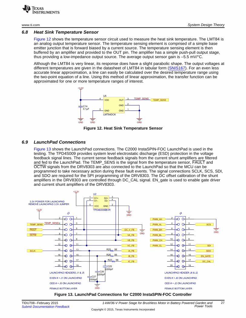
6.8 Heat Sink Temperature SensorFigure 12 shows the temperature sensor circuit used to measure the heat sink temperature. The LMT84 isan analog output temperature sensor. The temperature sensing element is comprised of a simple baseemitter junction that is forward biased by a current source. The temperature sensing element is thenbuffered by an amplifier and provided to the OUT pin. The amplifier has a simple push-pull output stage,thus providing a low-impedance output source. The average output sensor gain is –5.5 mV/°C.
Although the LMT84 is very linear, its response does have a slight parabolic shape. The output voltages atdifferent temperatures are given in the datasheet of LMT84 in tabular form (SNIS167). For an even lessaccurate linear approximation, a line can easily be calculated over the desired temperature range usingthe two-point equation of a line. Using this method of linear approximation, the transfer function can beapproximated for one or more temperature ranges of interest.
Figure 12. Heat Sink Temperature Sensor
6.9 LaunchPad ConnectionsFigure 13 shows the LaunchPad connections. The C2000 InstaSPIN-FOC LaunchPad is used in thetesting. The TPD4S009 provides system level electrostatic discharge (ESD) protection in the voltagefeedback signal lines. The current sense feedback signals from the current shunt amplifiers are filteredand fed to the LaunchPad. The TEMP_SENS is the signal from the temperature sensor, FAULT andOCTW signals from the DRV8303 are also connected to the LaunchPad so that the MCU can beprogrammed to take necessary action during these fault events. The signal connections SCLK, SCS, SDI,and SDO are required for the SPI programming of the DRV8303. The DC offset calibration of the shuntamplifiers in the DRV8303 are controlled through DC_CAL signal. EN_gate is used to enable gate driverand current shunt amplifiers of the DRV8303.
Figure 13. LaunchPad Connections for C2000 InstaSPIN-FOC Controller
27TIDU708–February 2015 1-kW/36-V Power Stage for Brushless Motor in Battery Powered Garden andPower ToolsSubmit Documentation Feedback
Copyright © 2015, Texas Instruments Incorporated
OCTW
FAULT
OCTW
+3.3V+3.3V
+3.3V
1
2
C1
A2
RED
D2
D-LED_0805
G1
S2
D3
P_CHQ2
GND
330R4
C1
A2
YELLOW
D1
D-LED_0805
GND
330R1
G1
S2
D3
P_CHQ1
+3.3V
FAULT
3.3kR2
3.3kR3
System Design Theory www.ti.com
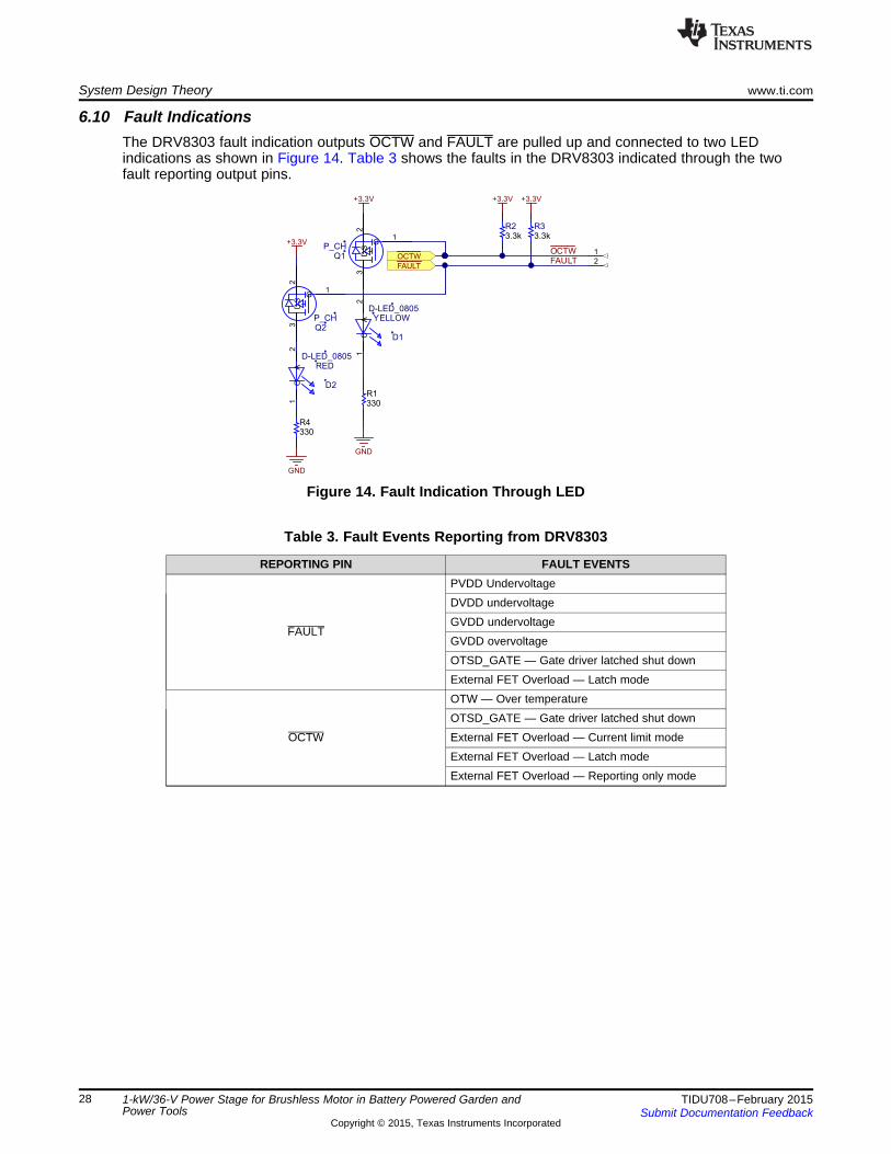
6.10 Fault IndicationsThe DRV8303 fault indication outputs OCTW and FAULT are pulled up and connected to two LEDindications as shown in Figure 14. Table 3 shows the faults in the DRV8303 indicated through the twofault reporting output pins.
Figure 14. Fault Indication Through LED
Table 3. Fault Events Reporting from DRV8303
REPORTING PIN FAULT EVENTSPVDD UndervoltageDVDD undervoltageGVDD undervoltage
FAULTGVDD overvoltageOTSD_GATE — Gate driver latched shut downExternal FET Overload — Latch modeOTW — Over temperatureOTSD_GATE — Gate driver latched shut down
OCTW External FET Overload — Current limit modeExternal FET Overload — Latch modeExternal FET Overload — Reporting only mode
28 1-kW/36-V Power Stage for Brushless Motor in Battery Powered Garden and TIDU708–February 2015Power Tools Submit Documentation Feedback
Copyright © 2015, Texas Instruments Incorporated

www.ti.com Getting Started Firmware
7 Getting Started FirmwareThe InstaSPIN-FOC is selected as it is easy to work with motors with unknown parameters. The MCUfirmware for C2000 Piccolo LaunchPad is taken from MotorWare™ software. MotorWare contains therequired projects and libraries to use TI’s InstaSPIN-FOC technology. MotorWare can be downloadedfrom http://www.ti.com/tool/motorware.
This design is compatible with "boostxldrv8301_revB" hardware and has the same pin configurations.Therefore, for Code Composer Studio™ (CCS) projects, use the projects under "boostxldrv8301_revB".After installing MotorWare, the projects can be located in this folder location:\motorware\motorware_1_01_00_13\sw\solutions\InstaSPIN_foc\boards\boostxldrv8301_revB\f28x\f2802xF\projects\ccs5
The projects are arranged in a series of labs. Lab9 implements a speed controller to perform the load testof the board. However, as a perquisite to this, Lab2c and Lab5a are run to tune the firmware for thereference design board and the motor. The following mentions the flow used to setup the firmware:• Lab2c is used to obtain the motor resistance, inductance and board offsets.• Lab5a is used to tune the PI controller of the current loop.• Lab9 is used for the load test.
The detailed procedure to build and run the lab is given in InstaSPIN Projects and Labs User’s Guideprovided inside MotorWare.
29TIDU708–February 2015 1-kW/36-V Power Stage for Brushless Motor in Battery Powered Garden andPower ToolsSubmit Documentation Feedback
Copyright © 2015, Texas Instruments Incorporated

Getting Started Firmware www.ti.com
7.1 Modifying user.hInstaSPIN-FOC libraries use a global header file user.h, which contains many important parameters usedin InstaSPIN-FOC. Some of these parameters values are dependent on the board and motor. Table 4 liststhe parameters that need to be changed to make the firmware compatible with the reference design.
Table 4. Parameters in user.h to Tune Based on Motor and Board
PARAMETER VALUE COMMENTUSER_IQ_FULL_SCALE_FREQ_Hz 800 > (Maximum RPM × Poles) / 120USER_IQ_FULL_SCALE_VOLTAGE_V 48 See Section 6.6USER_ADC_FULL_SCALE_VOLTAGE_V 55.5 See Section 6.6USER_IQ_FULL_SCALE_CURRENT_A 85 See Section 6.5USER_ADC_FULL_SCALE_CURRENT_A 165 See Section 6.5USER_NUM_CURRENT_SENSORS 3 Number of current sensorsI_A_offset 0.521301746 In Lab2c, the offset is computed and stored in user.h for use inI_B_offset 0.523253679 other labs.I_C_offset 0.50654459
In Lab2c, the offset is computed and stored in user.h for use inV_A_offset 0.44593966 other labs.V_B_offset 0.447788179V_C_offset 0.442513049
For Lab2c, identification is done using higher PWM frequencyUSER_PWM_FREQ_kHz 60.0 of 60 kHz as it helps identifying low inductance motors.USER_VOLTAGE_FILTER_POLE_Hz 769.164 See Section 6.5
MOTOR_Type_PUSER_MOTOR_TYPE Motor type — Permanent magnet motorsmUSER_MOTOR_NUM_POLE_PAIRS 8 Number of pole pairs in the motorUSER_MOTOR_Rr NULL Not applicable for PMSMUSER_MOTOR_Rs 0.006022509 Values obtained from Lab2c identification.
Identified motor phase to neutral resistance is 60 mΩ andUSER_MOTOR_Ls_d 3.79984E-05 average stator inductance is 38 µH.USER_MOTOR_Ls_q 3.79984E-05USER_MOTOR_RATED_FLUX 0.05358878USER_MOTOR_MAGNETIZING_CURRENT NULL Not applicable for PMSM
Maximum current used for Rs estimation in motor identification.USER_MOTOR_RES_EST_CURRENT 5 Use 10 to 20% of rated current.Maximum current (negative Amperes, float) used for LsUSER_MOTOR_IND_EST –5 estimation, use just enough to enable rotation.Sets a limit on the maximum current command output of the
USER_MOTOR_MAX_CURRENT 80 provided speed PI controller to the IQ controller, used duringidentification and run-time.Default value is 20 Hz, but this can be increased to get a betterUSER_MOTOR_FLUX_EST_FREQ_Hz 20 estimation values in Lab2c.
30 1-kW/36-V Power Stage for Brushless Motor in Battery Powered Garden and TIDU708–February 2015Power Tools Submit Documentation Feedback
Copyright © 2015, Texas Instruments Incorporated

www.ti.com Getting Started Firmware
7.2 Configuring DRV8303 RegistersThe InstaSPIN-FOC project sets up registers in the DRV8303 using the SPI peripheral TMS320F2027.The InstaSPIN-FOC projects use two source files by name drv8301.h and drv8301.c for configuringDRV8303. These files contains the DRV8303 register details and function to read and write to DRV8303using the SPI peripheral. Project uses DRV8301_setupSpi function to initialize the DRV8303 at start up.The control register configuration for DRV8303 is given below.
// Update Control Register 1drvRegNamea= DRV8301_RegName_Control_1;drvDataNew a= (DRV8301_PeakCurrent_0p70_A | \
DRV8301_Reset_Normal | \DRV8301_PwmMode_Six_Inputs | \DRV8301_OcMode_CurrentLimit | \DRV8301_VdsLevel_1p043_V);
// Update Control Register 2drvRegNamea= DRV8301_RegName_Control_2;drvDataNew a= (DRV8301_OcTwMode_Both | \
DRV8301_ShuntAmpGain_20VpV | \DRV8301_DcCalMode_Ch1_Load | \DRV8301_DcCalMode_Ch2_Load | \DRV8301_OcOffTimeMode_Normal);
Refer to the DRV8303 datasheet to see the full list of the setup options available (SLOS846).
31TIDU708–February 2015 1-kW/36-V Power Stage for Brushless Motor in Battery Powered Garden andPower ToolsSubmit Documentation Feedback
Copyright © 2015, Texas Instruments Incorporated
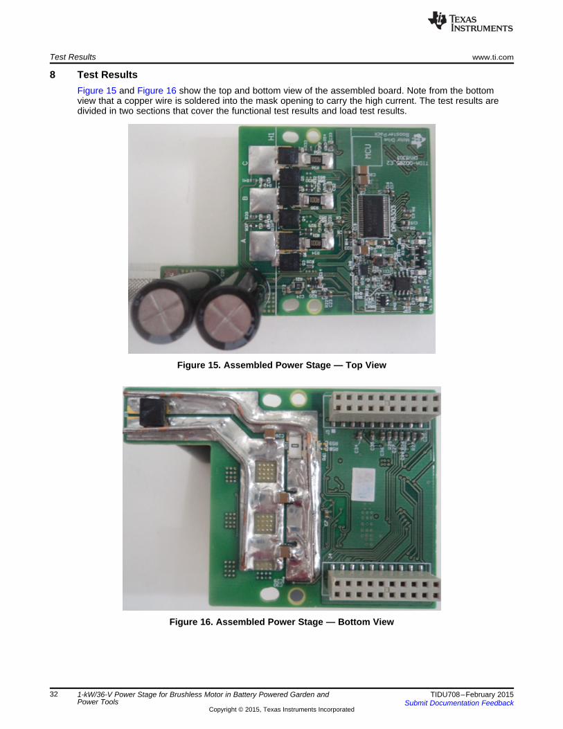
Test Results www.ti.com
8 Test ResultsFigure 15 and Figure 16 show the top and bottom view of the assembled board. Note from the bottomview that a copper wire is soldered into the mask opening to carry the high current. The test results aredivided in two sections that cover the functional test results and load test results.
Figure 15. Assembled Power Stage — Top View
Figure 16. Assembled Power Stage — Bottom View
32 1-kW/36-V Power Stage for Brushless Motor in Battery Powered Garden and TIDU708–February 2015Power Tools Submit Documentation Feedback
Copyright © 2015, Texas Instruments Incorporated
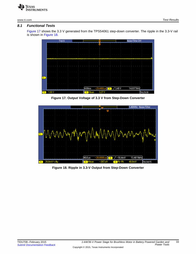
www.ti.com Test Results
8.1 Functional TestsFigure 17 shows the 3.3 V generated from the TPS54061 step-down converter. The ripple in the 3.3-V railis shown in Figure 18.
Figure 17. Output Voltage of 3.3 V from Step-Down Converter
Figure 18. Ripple in 3.3-V Output from Step-Down Converter
33TIDU708–February 2015 1-kW/36-V Power Stage for Brushless Motor in Battery Powered Garden andPower ToolsSubmit Documentation Feedback
Copyright © 2015, Texas Instruments Incorporated
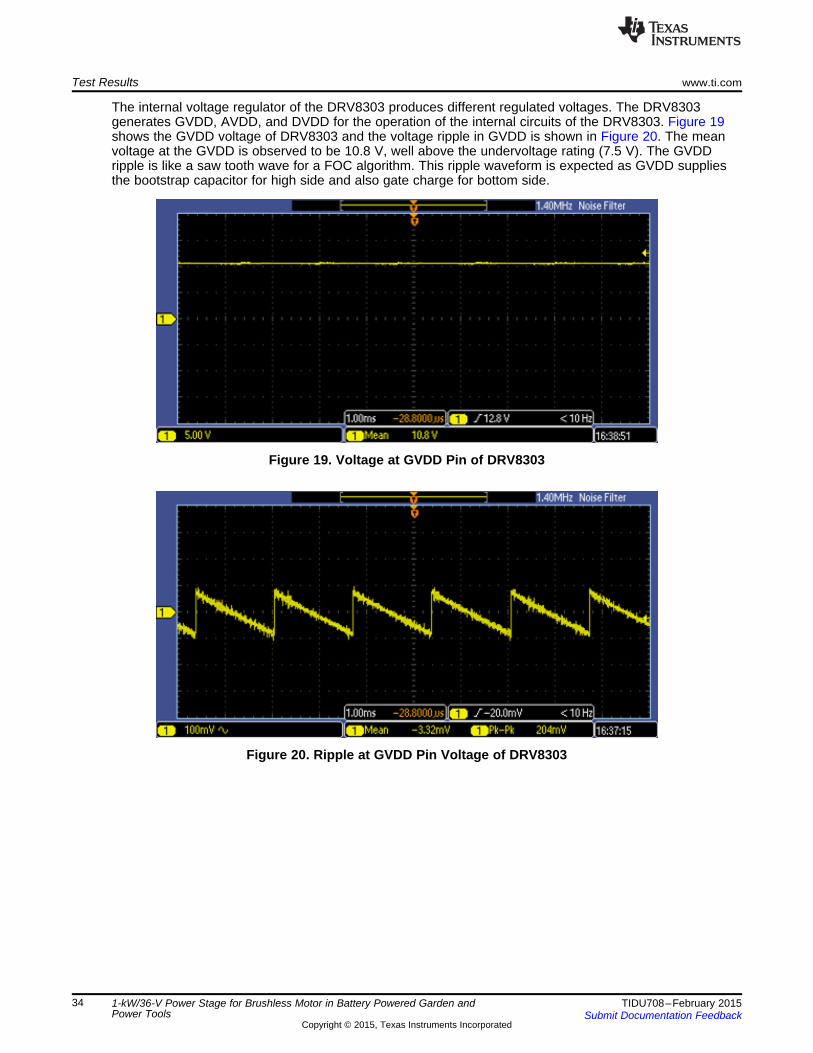
Test Results www.ti.com
The internal voltage regulator of the DRV8303 produces different regulated voltages. The DRV8303generates GVDD, AVDD, and DVDD for the operation of the internal circuits of the DRV8303. Figure 19shows the GVDD voltage of DRV8303 and the voltage ripple in GVDD is shown in Figure 20. The meanvoltage at the GVDD is observed to be 10.8 V, well above the undervoltage rating (7.5 V). The GVDDripple is like a saw tooth wave for a FOC algorithm. This ripple waveform is expected as GVDD suppliesthe bootstrap capacitor for high side and also gate charge for bottom side.
Figure 19. Voltage at GVDD Pin of DRV8303
Figure 20. Ripple at GVDD Pin Voltage of DRV8303
34 1-kW/36-V Power Stage for Brushless Motor in Battery Powered Garden and TIDU708–February 2015Power Tools Submit Documentation Feedback
Copyright © 2015, Texas Instruments Incorporated
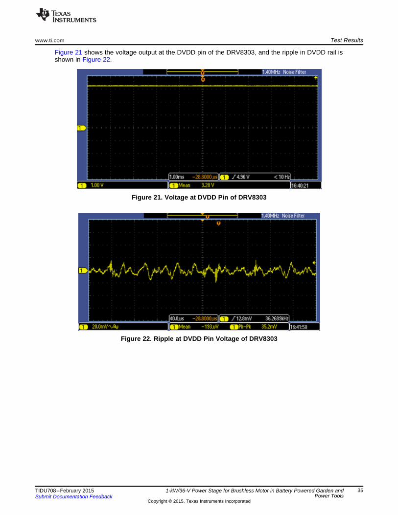
www.ti.com Test Results
Figure 21 shows the voltage output at the DVDD pin of the DRV8303, and the ripple in DVDD rail isshown in Figure 22.
Figure 21. Voltage at DVDD Pin of DRV8303
Figure 22. Ripple at DVDD Pin Voltage of DRV8303
35TIDU708–February 2015 1-kW/36-V Power Stage for Brushless Motor in Battery Powered Garden andPower ToolsSubmit Documentation Feedback
Copyright © 2015, Texas Instruments Incorporated
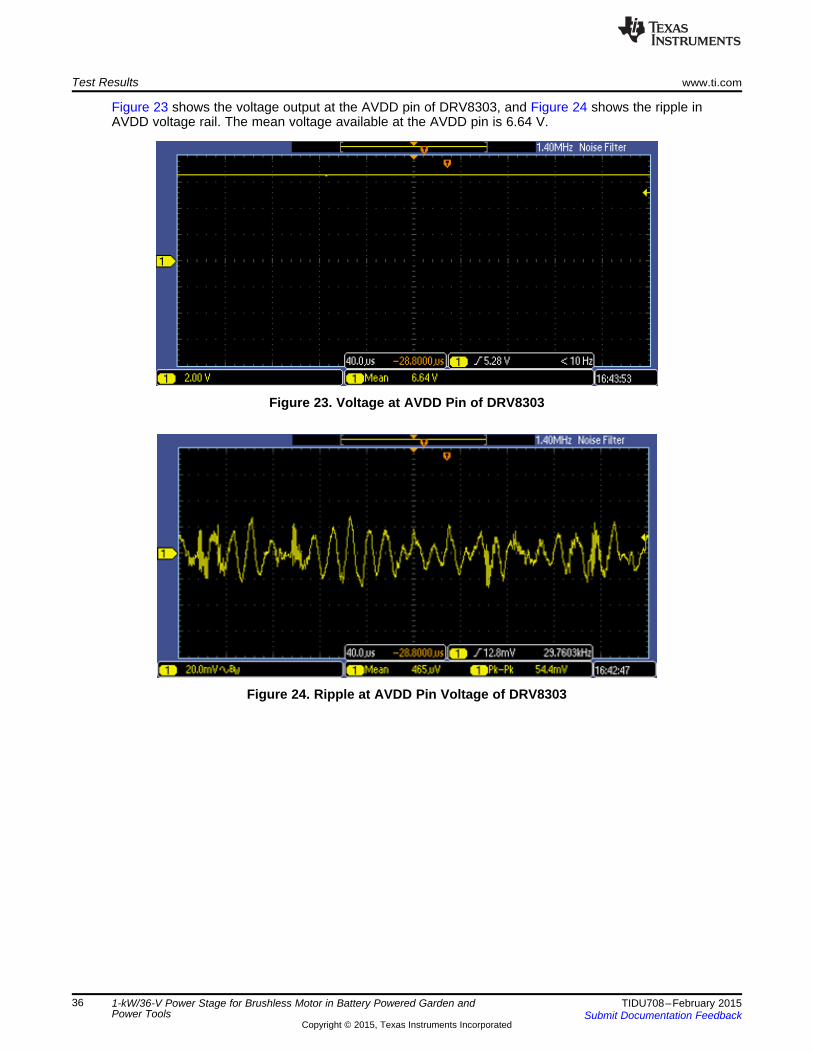
Test Results www.ti.com
Figure 23 shows the voltage output at the AVDD pin of DRV8303, and Figure 24 shows the ripple inAVDD voltage rail. The mean voltage available at the AVDD pin is 6.64 V.
Figure 23. Voltage at AVDD Pin of DRV8303
Figure 24. Ripple at AVDD Pin Voltage of DRV8303
36 1-kW/36-V Power Stage for Brushless Motor in Battery Powered Garden and TIDU708–February 2015Power Tools Submit Documentation Feedback
Copyright © 2015, Texas Instruments Incorporated
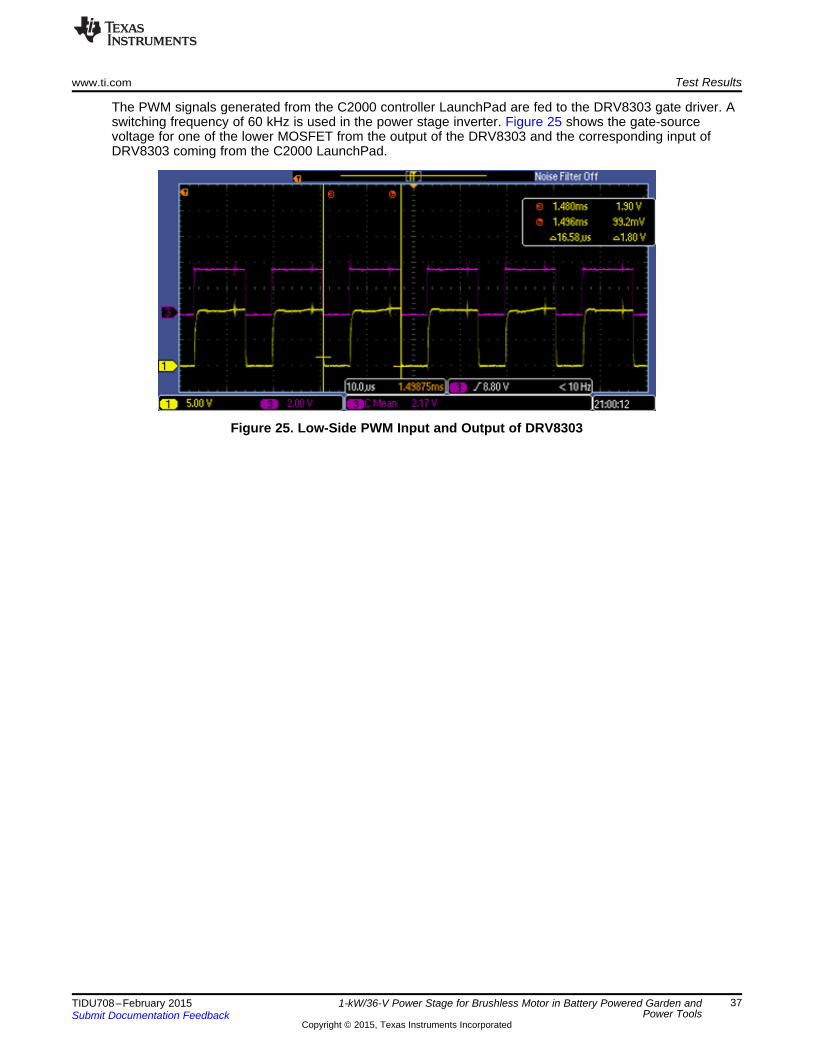
www.ti.com Test Results
The PWM signals generated from the C2000 controller LaunchPad are fed to the DRV8303 gate driver. Aswitching frequency of 60 kHz is used in the power stage inverter. Figure 25 shows the gate-sourcevoltage for one of the lower MOSFET from the output of the DRV8303 and the corresponding input ofDRV8303 coming from the C2000 LaunchPad.
Figure 25. Low-Side PWM Input and Output of DRV8303
37TIDU708–February 2015 1-kW/36-V Power Stage for Brushless Motor in Battery Powered Garden andPower ToolsSubmit Documentation Feedback
Copyright © 2015, Texas Instruments Incorporated
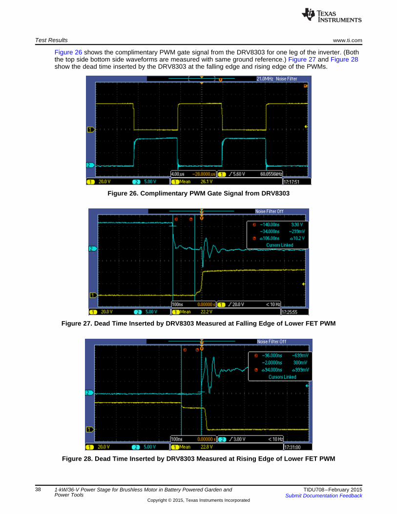
Test Results www.ti.com
Figure 26 shows the complimentary PWM gate signal from the DRV8303 for one leg of the inverter. (Boththe top side bottom side waveforms are measured with same ground reference.) Figure 27 and Figure 28show the dead time inserted by the DRV8303 at the falling edge and rising edge of the PWMs.
Figure 26. Complimentary PWM Gate Signal from DRV8303
Figure 27. Dead Time Inserted by DRV8303 Measured at Falling Edge of Lower FET PWM
Figure 28. Dead Time Inserted by DRV8303 Measured at Rising Edge of Lower FET PWM
38 1-kW/36-V Power Stage for Brushless Motor in Battery Powered Garden and TIDU708–February 2015Power Tools Submit Documentation Feedback
Copyright © 2015, Texas Instruments Incorporated
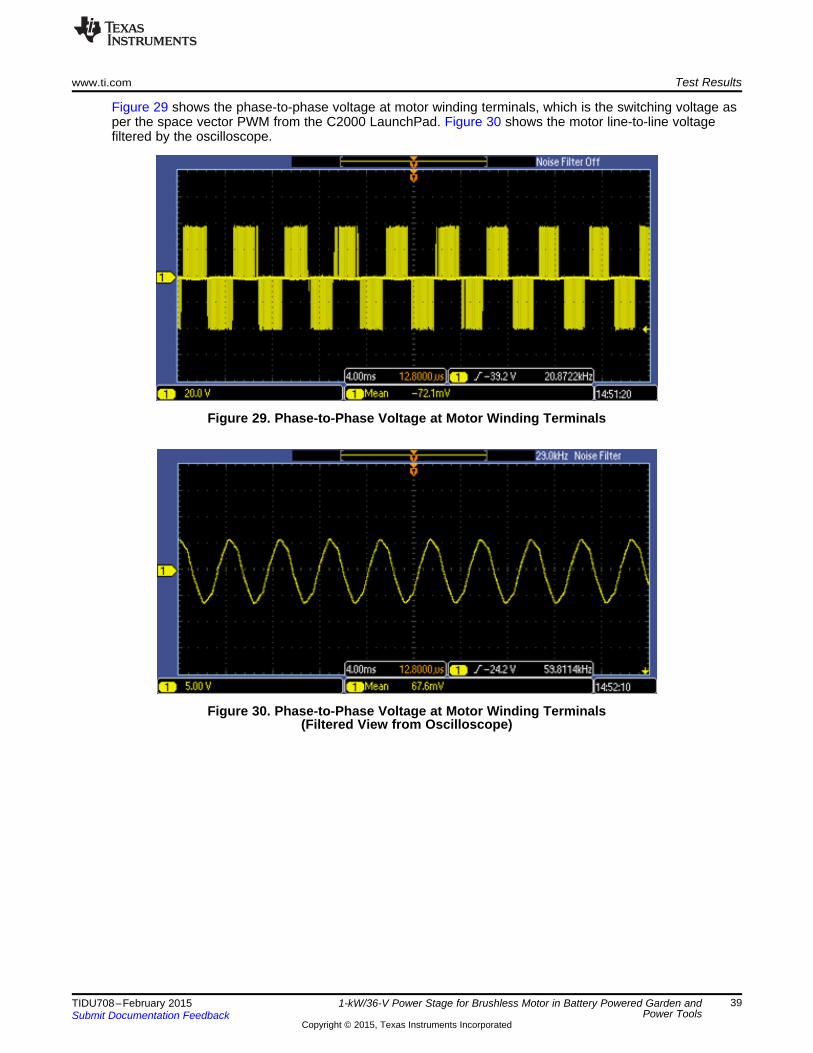
www.ti.com Test Results
Figure 29 shows the phase-to-phase voltage at motor winding terminals, which is the switching voltage asper the space vector PWM from the C2000 LaunchPad. Figure 30 shows the motor line-to-line voltagefiltered by the oscilloscope.
Figure 29. Phase-to-Phase Voltage at Motor Winding Terminals
Figure 30. Phase-to-Phase Voltage at Motor Winding Terminals(Filtered View from Oscilloscope)
39TIDU708–February 2015 1-kW/36-V Power Stage for Brushless Motor in Battery Powered Garden andPower ToolsSubmit Documentation Feedback
Copyright © 2015, Texas Instruments Incorporated
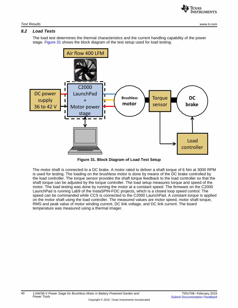
DC power
supply
36 to 42 V
Load
controller
C2000
LaunchPad
+
Motor power
stage
DC
brake
Torque
sensor
Brushless
motor
Air flow 400 LFM
Test Results www.ti.com
8.2 Load TestsThe load test determines the thermal characteristics and the current handling capability of the powerstage. Figure 31 shows the block diagram of the test setup used for load testing.
Figure 31. Block Diagram of Load Test Setup
The motor shaft is connected to a DC brake. A motor rated to deliver a shaft torque of 6 Nm at 3000 RPMis used for testing. The loading on the brushless motor is done by means of the DC brake controlled bythe load controller. The torque sensor provides the shaft torque feedback to the load controller so that theshaft torque can be adjusted by the torque controller. The load setup measures torque and speed of themotor. The load testing was done by running the motor at a constant speed. The firmware on the C2000LaunchPad is running Lab9 of the InstaSPIN-FOC projects, which is a closed loop speed control. Thespeed can be commanded while CCS is connected to the C2000 LaunchPad. A constant torque is appliedon the motor shaft using the load controller. The measured values are motor speed, motor shaft torque,RMS and peak value of motor winding current, DC link voltage, and DC link current. The boardtemperature was measured using a thermal imager.
40 1-kW/36-V Power Stage for Brushless Motor in Battery Powered Garden and TIDU708–February 2015Power Tools Submit Documentation Feedback
Copyright © 2015, Texas Instruments Incorporated
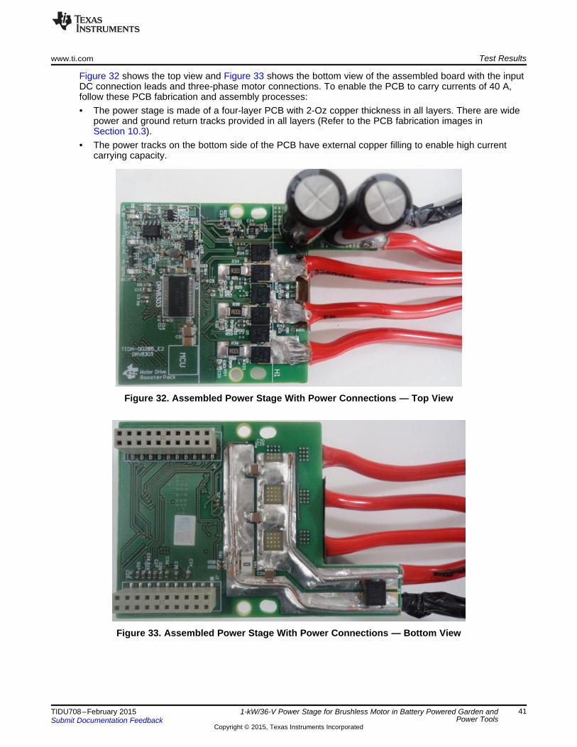
www.ti.com Test Results
Figure 32 shows the top view and Figure 33 shows the bottom view of the assembled board with the inputDC connection leads and three-phase motor connections. To enable the PCB to carry currents of 40 A,follow these PCB fabrication and assembly processes:• The power stage is made of a four-layer PCB with 2-Oz copper thickness in all layers. There are wide
power and ground return tracks provided in all layers (Refer to the PCB fabrication images inSection 10.3).
• The power tracks on the bottom side of the PCB have external copper filling to enable high currentcarrying capacity.
Figure 32. Assembled Power Stage With Power Connections — Top View
Figure 33. Assembled Power Stage With Power Connections — Bottom View
41TIDU708–February 2015 1-kW/36-V Power Stage for Brushless Motor in Battery Powered Garden andPower ToolsSubmit Documentation Feedback
Copyright © 2015, Texas Instruments Incorporated
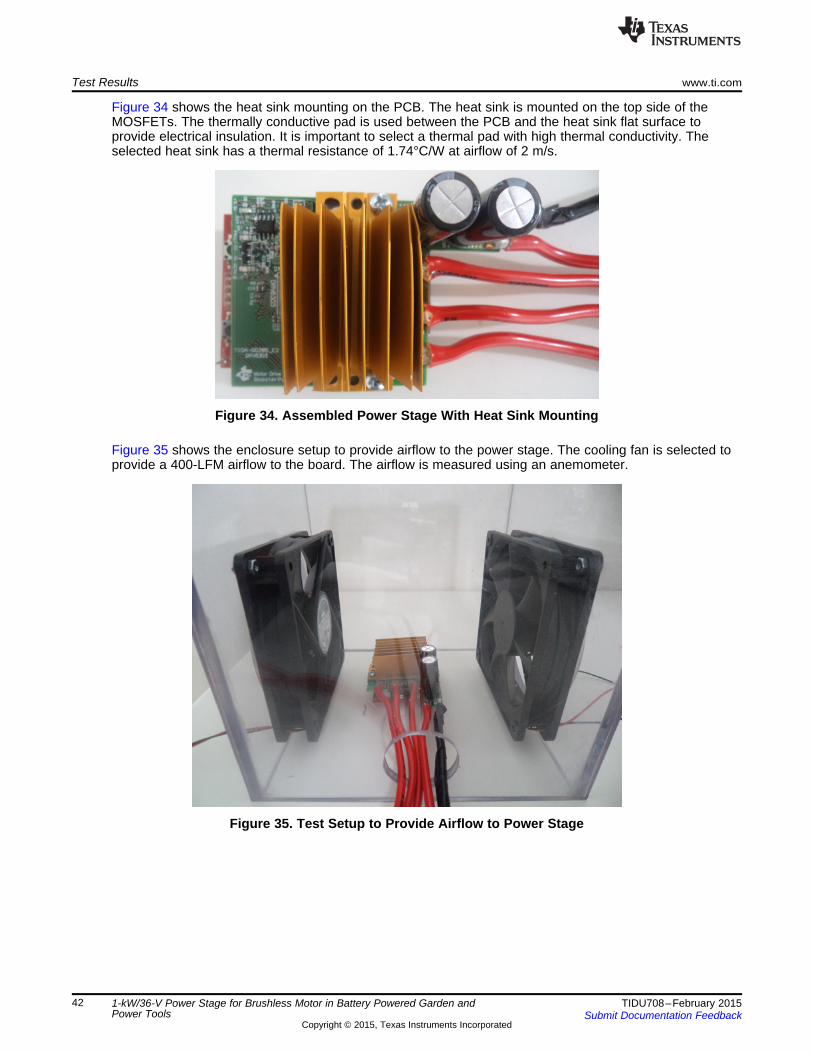
Test Results www.ti.com
Figure 34 shows the heat sink mounting on the PCB. The heat sink is mounted on the top side of theMOSFETs. The thermally conductive pad is used between the PCB and the heat sink flat surface toprovide electrical insulation. It is important to select a thermal pad with high thermal conductivity. Theselected heat sink has a thermal resistance of 1.74°C/W at airflow of 2 m/s.
Figure 34. Assembled Power Stage With Heat Sink Mounting
Figure 35 shows the enclosure setup to provide airflow to the power stage. The cooling fan is selected toprovide a 400-LFM airflow to the board. The airflow is measured using an anemometer.
Figure 35. Test Setup to Provide Airflow to Power Stage
42 1-kW/36-V Power Stage for Brushless Motor in Battery Powered Garden and TIDU708–February 2015Power Tools Submit Documentation Feedback
Copyright © 2015, Texas Instruments Incorporated
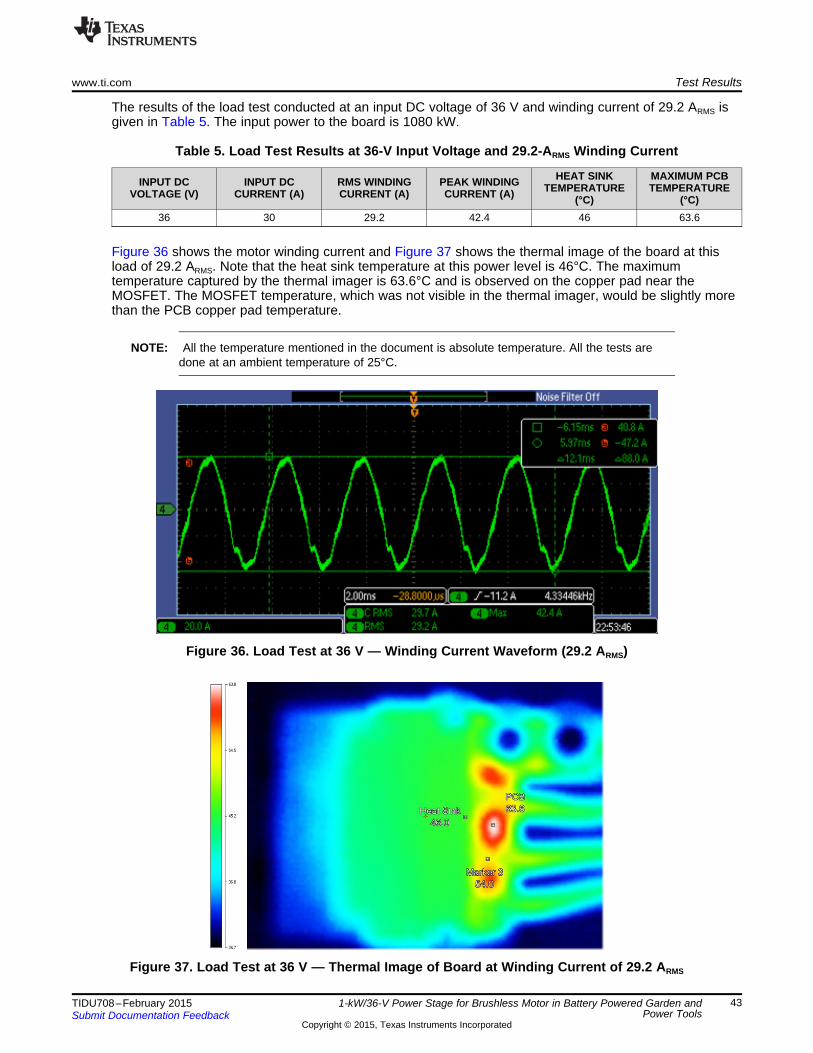
www.ti.com Test Results
The results of the load test conducted at an input DC voltage of 36 V and winding current of 29.2 ARMS isgiven in Table 5. The input power to the board is 1080 kW.
Table 5. Load Test Results at 36-V Input Voltage and 29.2-ARMS Winding Current
HEAT SINK MAXIMUM PCBINPUT DC INPUT DC RMS WINDING PEAK WINDING TEMPERATURE TEMPERATUREVOLTAGE (V) CURRENT (A) CURRENT (A) CURRENT (A) (°C) (°C)36 30 29.2 42.4 46 63.6
Figure 36 shows the motor winding current and Figure 37 shows the thermal image of the board at thisload of 29.2 ARMS. Note that the heat sink temperature at this power level is 46°C. The maximumtemperature captured by the thermal imager is 63.6°C and is observed on the copper pad near theMOSFET. The MOSFET temperature, which was not visible in the thermal imager, would be slightly morethan the PCB copper pad temperature.
NOTE: All the temperature mentioned in the document is absolute temperature. All the tests aredone at an ambient temperature of 25°C.
Figure 36. Load Test at 36 V — Winding Current Waveform (29.2 ARMS)
Figure 37. Load Test at 36 V — Thermal Image of Board at Winding Current of 29.2 ARMS
43TIDU708–February 2015 1-kW/36-V Power Stage for Brushless Motor in Battery Powered Garden andPower ToolsSubmit Documentation Feedback
Copyright © 2015, Texas Instruments Incorporated
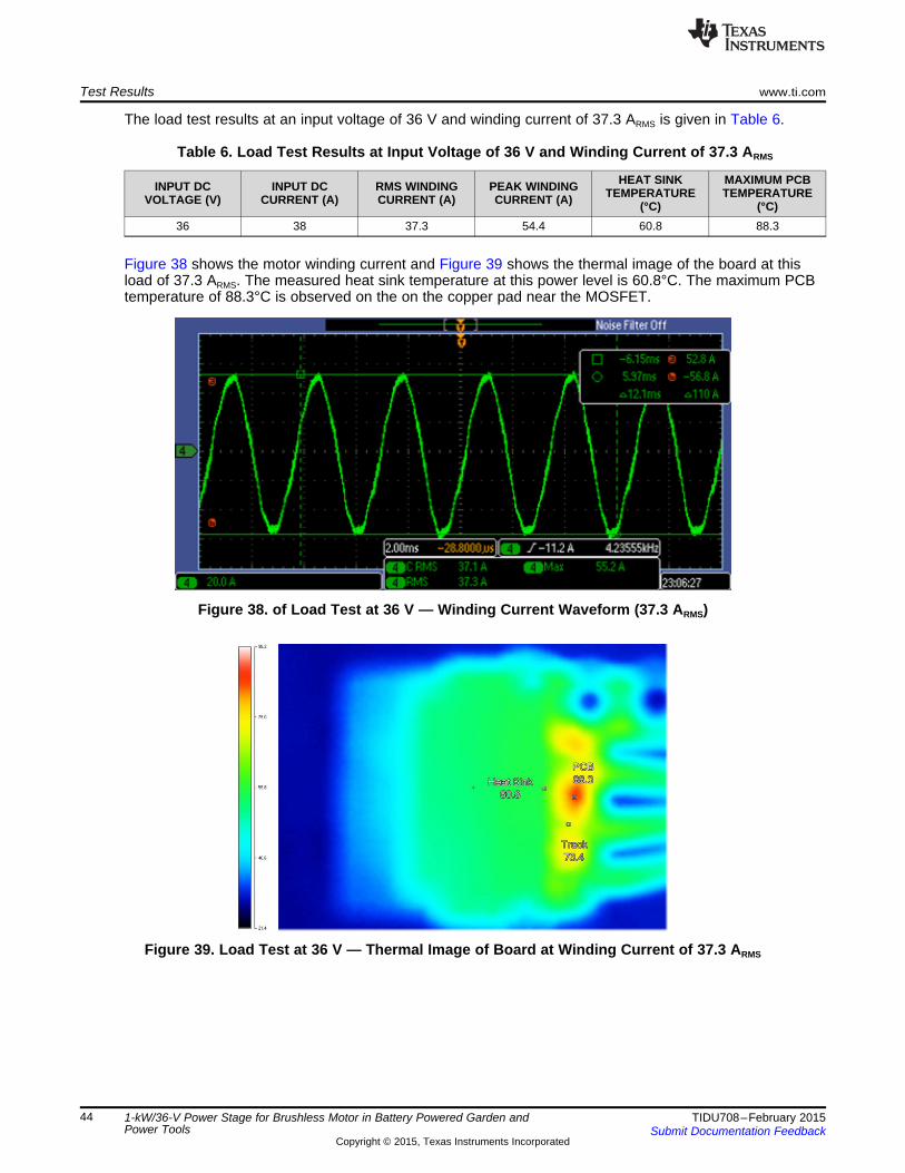
Test Results www.ti.com
The load test results at an input voltage of 36 V and winding current of 37.3 ARMS is given in Table 6.
Table 6. Load Test Results at Input Voltage of 36 V and Winding Current of 37.3 ARMS
HEAT SINK MAXIMUM PCBINPUT DC INPUT DC RMS WINDING PEAK WINDING TEMPERATURE TEMPERATUREVOLTAGE (V) CURRENT (A) CURRENT (A) CURRENT (A) (°C) (°C)36 38 37.3 54.4 60.8 88.3
Figure 38 shows the motor winding current and Figure 39 shows the thermal image of the board at thisload of 37.3 ARMS. The measured heat sink temperature at this power level is 60.8°C. The maximum PCBtemperature of 88.3°C is observed on the on the copper pad near the MOSFET.
Figure 38. of Load Test at 36 V — Winding Current Waveform (37.3 ARMS)
Figure 39. Load Test at 36 V — Thermal Image of Board at Winding Current of 37.3 ARMS
44 1-kW/36-V Power Stage for Brushless Motor in Battery Powered Garden and TIDU708–February 2015Power Tools Submit Documentation Feedback
Copyright © 2015, Texas Instruments Incorporated
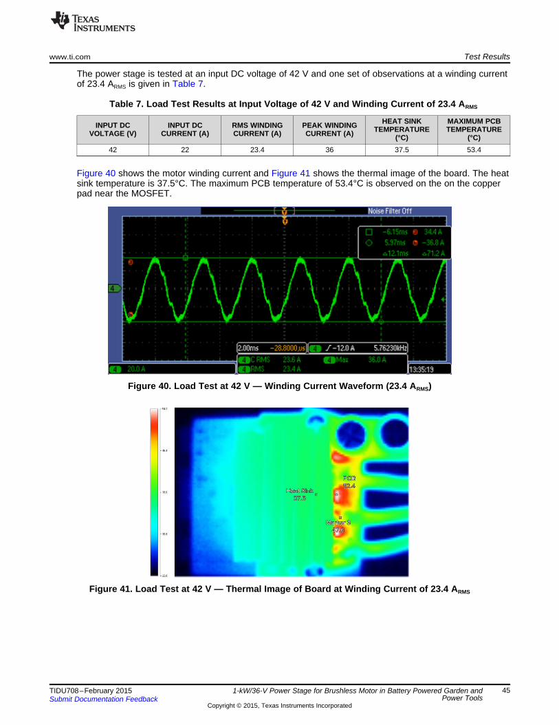
www.ti.com Test Results
The power stage is tested at an input DC voltage of 42 V and one set of observations at a winding currentof 23.4 ARMS is given in Table 7.
Table 7. Load Test Results at Input Voltage of 42 V and Winding Current of 23.4 ARMS
HEAT SINK MAXIMUM PCBINPUT DC INPUT DC RMS WINDING PEAK WINDING TEMPERATURE TEMPERATUREVOLTAGE (V) CURRENT (A) CURRENT (A) CURRENT (A) (°C) (°C)42 22 23.4 36 37.5 53.4
Figure 40 shows the motor winding current and Figure 41 shows the thermal image of the board. The heatsink temperature is 37.5°C. The maximum PCB temperature of 53.4°C is observed on the on the copperpad near the MOSFET.
Figure 40. Load Test at 42 V — Winding Current Waveform (23.4 ARMS)
Figure 41. Load Test at 42 V — Thermal Image of Board at Winding Current of 23.4 ARMS
45TIDU708–February 2015 1-kW/36-V Power Stage for Brushless Motor in Battery Powered Garden andPower ToolsSubmit Documentation Feedback
Copyright © 2015, Texas Instruments Incorporated
Test Results www.ti.com
The complete load test results at 36 V and at a motor speed of 2300 RPM is given in Table 8. The loadtest results at 42 V and at a motor speed of 2500 RPM is tabulated in Table 9.
Table 8. Load Test Results at Input Voltage of 36-V DC and 2300 RPM
MOTOR MAXIMUM PCBINPUT DC RMS WINDING PEAK WINDING MOTOR SHAFT DC INPUTOUTPUT TEMPERATURECURRENT (A) CURRENT (A) CURRENT (A) TORQUE (Nm) POWER (W)POWER (W) (°C)6.4 6.26 11.6 0 0 230.4 3210 9.75 16.4 0.55 132.99 360 3312 11.8 18.8 0.85 205.52 432 35
14.1 13.7 21.6 1.15 277.96 507.6 3716 15.7 24 1.43 345.68 576 3918 17.6 26.4 1.72 415.85 648 41
20.1 19.7 28.8 2.02 488.25 723.6 4422 21.7 32.2 2.3 556.27 792 4724 23.9 33.6 2.573 621.47 864 5126 25.9 36 2.86 691.45 936 5528 27.8 39.2 3.15 761.68 1008 5930 29.2 42.4 3.4 822.27 1080 6432 31.2 44.8 3.66 885.12 1152 6934 33.3 48 3.94 952.88 1224 7436 35.6 52 4.22 1020.21 1296 8138 37.3 54.4 4.48 1083.8 1368 89
Table 9. Load Test Results at Input Voltage of 42-V DC and 2500 RPM
MOTOR MAXIMUM PCBINPUT DC RMS WINDING PEAK WINDING MOTOR SHAFT DC INPUTOUTPUT TEMPERATURECURRENT (A) CURRENT (A) CURRENT (A) TORQUE (Nm) POWER (W)POWER (W) (°C)7.7 7.74 15.2 0 0 323.4 3210 10.2 18 0.4 104.61 420 33
12.1 12.4 21.2 0.76 198.65 508.2 3614.1 14.6 24 1.12 293.84 592.2 3916 16.7 27.2 1.45 379.31 672 42
18.1 18.8 29.6 1.77 469.86 760.2 4620 21.1 32.8 2.09 546.83 840 5022 23.4 36 2.42 633.05 924 5724 25.32 38.6 2.56 726.98 1008 6426 27.5 41.5 2.87 816.34 1092 74
46 1-kW/36-V Power Stage for Brushless Motor in Battery Powered Garden and TIDU708–February 2015Power Tools Submit Documentation Feedback
Copyright © 2015, Texas Instruments Incorporated

RMS Winding Current (A)
Maxim
um
Bo
ard
Tem
pera
ture
(0C
)
5 10 15 20 25 30 35 4030
40
50
60
70
80
90CSD19502Q5B (RDS_ON = 3.4 mΩ)CSD18540Q5B (RDS_ON = 1.8 mΩ)
RMS Winding Current (A)
Maxim
um
Board
Tem
pera
ture
(0C
)
5 10 15 20 25 30 35 4030
40
50
60
70
80
90
www.ti.com Test Results
Figure 42 shows the variation of the maximum temperature observed on the board (by the thermal imager)with the winding current. The maximum temperature is observed on the PCB copper pad near theMOSFET. The MOSFET temperature will be slightly more than the maximum observed temperature(MOSFETs are not visible in the thermal imager due to the heat sink).
Figure 42. Winding Current versus Maximum Temperature Observed on Board
The design uses CSD18540Q5B rated for 60 V with a RDS_ON of 1.8 mΩ. Alternatively, the thermalperformance of the power stage also evaluated with CSD19502Q5B NEXFETs with higher voltage ratingand consequently a higher RDS_ON. The FET CSD19502Q5B is rated for 80 V with a RDS_ON of 3.4 mΩ. Boththe MOSFETs are available in the SON5x6 package. Figure 43 shows the variation of the maximumtemperature observed on the board with the winding current for the two evaluated FETs. The maximumtemperature is observed on the PCB copper pad near the MOSFET.
Figure 43. Comparison of Temperature Rise in Power Stage Tested With Two Different MOSFETs
47TIDU708–February 2015 1-kW/36-V Power Stage for Brushless Motor in Battery Powered Garden andPower ToolsSubmit Documentation Feedback
Copyright © 2015, Texas Instruments Incorporated
DC power
supply
20 V Electronic load
Overload
current
Test Results www.ti.com
8.3 Overcurrent Protection TestThe current through the motor power stage can exceed the rated value due to motor overload or motorstall condition. The DRV8303 implements an overcurrent protection using the MOSFET VDS sensing. Theoverload and stall conditions are simulated by using a electronic resistive load. Alternatively, the overloadand stall conditions could have been applied mechanically to the motor; in this case, the brake ratingshould not be exceeded. Therefore, a more practical approach is taken to inject an overload current in thepower stage.
A single leg of the power stage is connected to an electronic load and the return current is routed throughthe power supply negative terminal. The current path during an overload is indicated as the red line inFigure 44. The current flows in the top MOSFET during the test. The C2000 LaunchPad is setup togenerate a PWM with a constant duty period of 50% at 60 kHz and the overcurrent and fault responsefeature of the C2000 LaunchPad is not used.
Figure 44. Circuit for Testing Overcurrent Shutdown Feature of DRV8303
48 1-kW/36-V Power Stage for Brushless Motor in Battery Powered Garden and TIDU708–February 2015Power Tools Submit Documentation Feedback
Copyright © 2015, Texas Instruments Incorporated
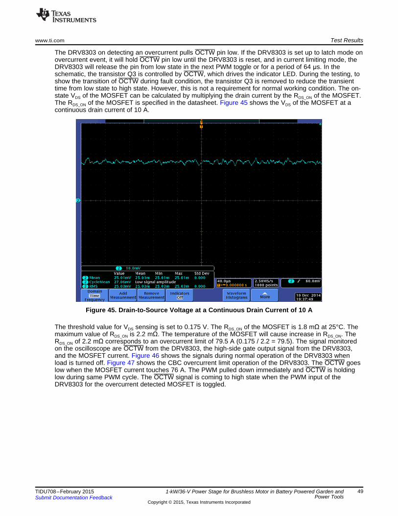
www.ti.com Test Results
The DRV8303 on detecting an overcurrent pulls OCTW pin low. If the DRV8303 is set up to latch mode onovercurrent event, it will hold OCTW pin low until the DRV8303 is reset, and in current limiting mode, theDRV8303 will release the pin from low state in the next PWM toggle or for a period of 64 μs. In theschematic, the transistor Q3 is controlled by OCTW, which drives the indicator LED. During the testing, toshow the transition of OCTW during fault condition, the transistor Q3 is removed to reduce the transienttime from low state to high state. However, this is not a requirement for normal working condition. The on-state VDS of the MOSFET can be calculated by multiplying the drain current by the RDS_ON of the MOSFET.The RDS_ON of the MOSFET is specified in the datasheet. Figure 45 shows the VDS of the MOSFET at acontinuous drain current of 10 A.
Figure 45. Drain-to-Source Voltage at a Continuous Drain Current of 10 A
The threshold value for VDS sensing is set to 0.175 V. The RDS_ON of the MOSFET is 1.8 mΩ at 25°C. Themaximum value of RDS_ON is 2.2 mΩ. The temperature of the MOSFET will cause increase in RDS_ON. TheRDS_ON of 2.2 mΩ corresponds to an overcurrent limit of 79.5 A (0.175 / 2.2 = 79.5). The signal monitoredon the oscilloscope are OCTW from the DRV8303, the high-side gate output signal from the DRV8303,and the MOSFET current. Figure 46 shows the signals during normal operation of the DRV8303 whenload is turned off. Figure 47 shows the CBC overcurrent limit operation of the DRV8303. The OCTW goeslow when the MOSFET current touches 76 A. The PWM pulled down immediately and OCTW is holdinglow during same PWM cycle. The OCTW signal is coming to high state when the PWM input of theDRV8303 for the overcurrent detected MOSFET is toggled.
49TIDU708–February 2015 1-kW/36-V Power Stage for Brushless Motor in Battery Powered Garden andPower ToolsSubmit Documentation Feedback
Copyright © 2015, Texas Instruments Incorporated
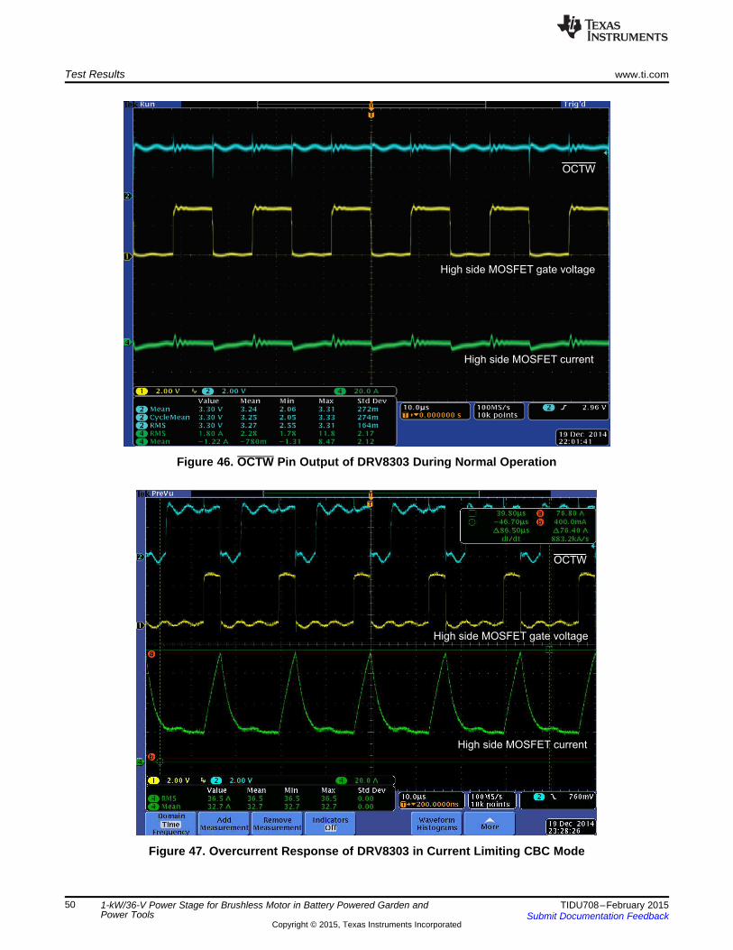
High side MOSFET current
High side MOSFET gate voltage
OCTW
High side MOSFET current
High side MOSFET gate voltage
OCTW
Test Results www.ti.com
Figure 46. OCTW Pin Output of DRV8303 During Normal Operation
Figure 47. Overcurrent Response of DRV8303 in Current Limiting CBC Mode
50 1-kW/36-V Power Stage for Brushless Motor in Battery Powered Garden and TIDU708–February 2015Power Tools Submit Documentation Feedback
Copyright © 2015, Texas Instruments Incorporated
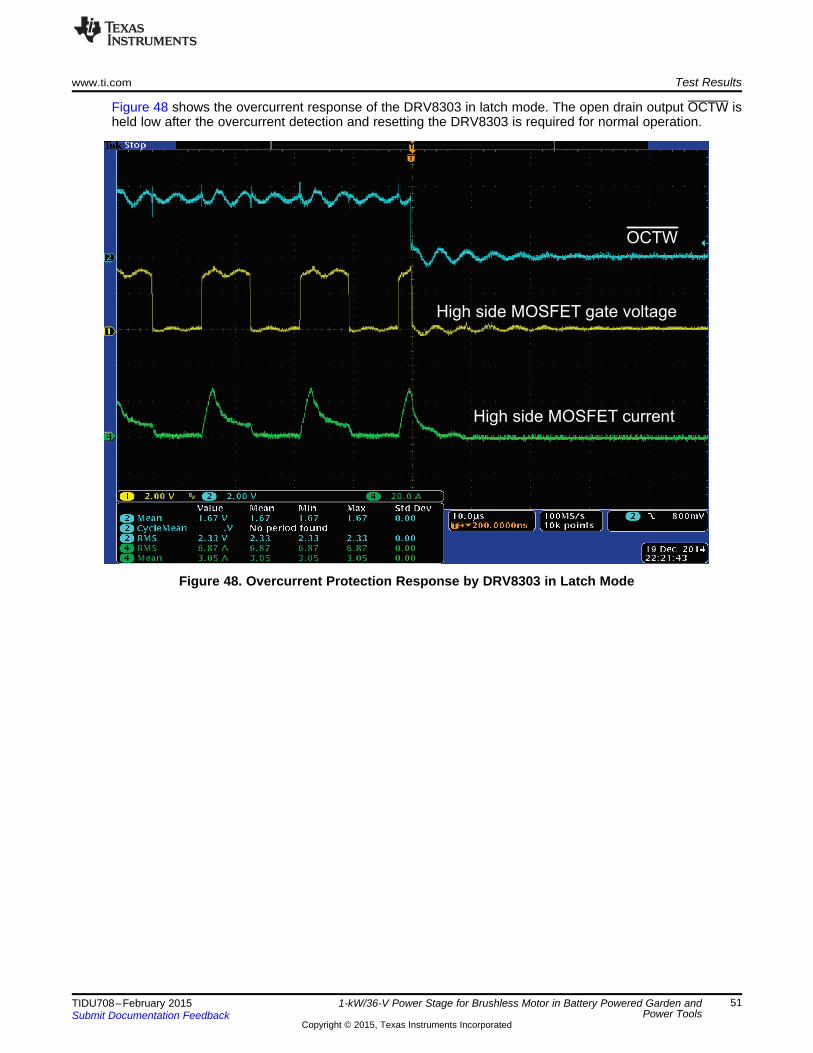
High side MOSFET current
High side MOSFET gate voltage
OCTW
www.ti.com Test Results
Figure 48 shows the overcurrent response of the DRV8303 in latch mode. The open drain output OCTW isheld low after the overcurrent detection and resetting the DRV8303 is required for normal operation.
Figure 48. Overcurrent Protection Response by DRV8303 in Latch Mode
51TIDU708–February 2015 1-kW/36-V Power Stage for Brushless Motor in Battery Powered Garden andPower ToolsSubmit Documentation Feedback
Copyright © 2015, Texas Instruments Incorporated

Using the Power Stage for Trapezoidal Control of BLDC Motors www.ti.com
9 Using the Power Stage for Trapezoidal Control of BLDC MotorsThe BLDC motor is conventionally defined as a permanent magnet motors with a trapezoidal BEMFwaveform shape and a PMSM is having a sinusoidal BEMF. Both motor types are synchronous machines.The only difference between them is the shape of the induced voltage.
In BLDC motors, trapezoidal control is used where only two phases are ON at a time and the third phaseis open. The phase windings are energized by square wave currents. In PMSM, sinusoidal control is usedwhere all the three phase winding of the motor is ON at a time and the windings are energized bysinusoidal currents. BLDC machines could be driven with sinusoidal currents and PMSM with square wavecurrents, but for better performance, PMSM should be excited by sinusoidal currents and BLDC machinesby square wave currents.
The trapezoidal control is simple and has less switching losses compared to sinusoidal control. Thecontrol structure (hardware and software) of a sinusoidal motor requires several current sensors andsinusoidal phase currents, which are hard to achieve with analog techniques. Trapezoidal control has thedisadvantage of commutation torque ripple.
To get the best performance out of the permanent magnet motor, identify the type of motor to apply themost appropriate type of control. In this reference design, sinusoidal control (InstaSPIN-FOC) is used tovalidate the performance of the power stage as the motor used for testing had a sinusoidal BEMF.However, the same power stage can be used to drive a BLDC motor with trapezoidal control using aC2000 controller. The power stage can also support a 30-ARMS phase winding current in trapezoidalcontrol.
52 1-kW/36-V Power Stage for Brushless Motor in Battery Powered Garden and TIDU708–February 2015Power Tools Submit Documentation Feedback
Copyright © 2015, Texas Instruments Incorporated
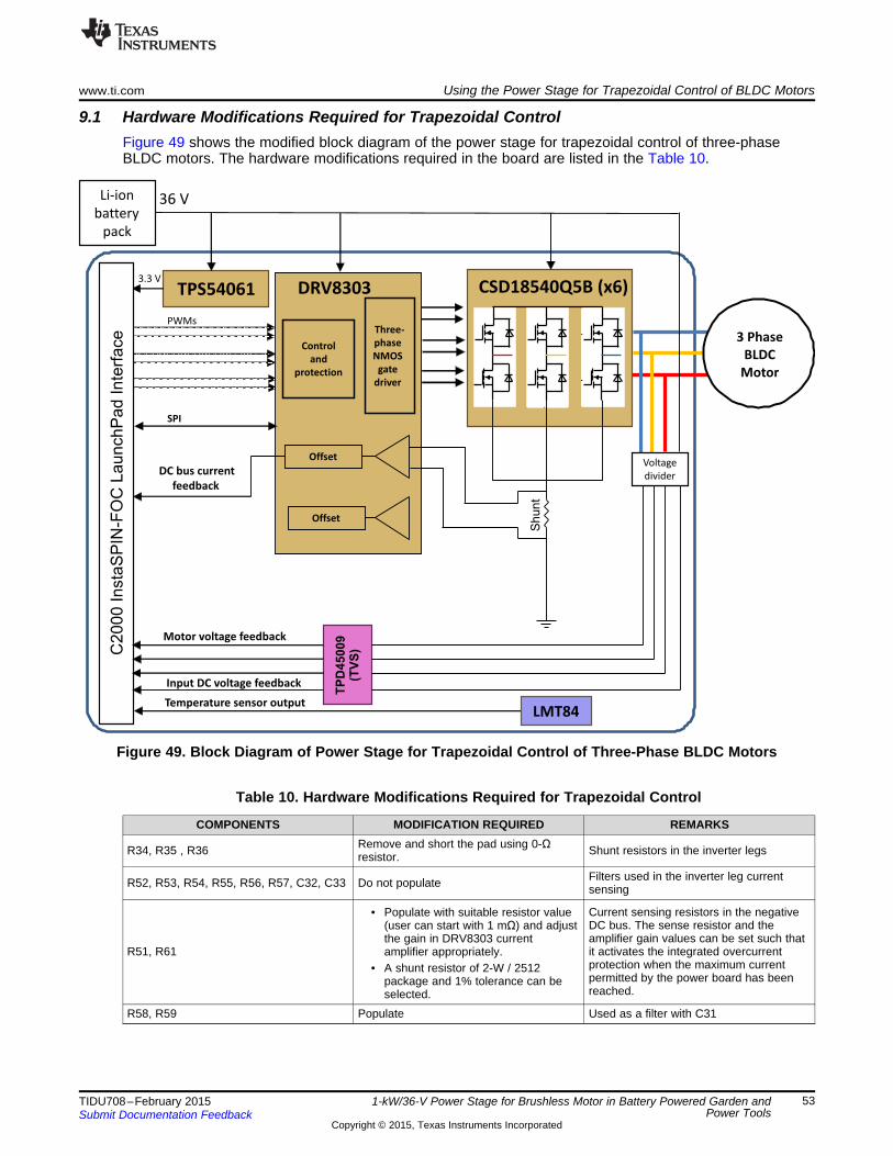
3 Phase
BLDC
Motor
Offset
Offset
3.3 V
PWMs
DRV8303
36 VLi-ion
battery
pack
SPI
Three-
phase
NMOS
gate
driver
Control
and
protection
Temperature sensor output
TPS54061
Voltage
divider
LMT84
Motor voltage feedback
DC bus current
feedback
CSD18540Q5B (x6)
Input DC voltage feedback
C2000 Insta
SP
IN-F
OC
LaunchP
ad Inte
rface
Shunt
TP
D45009
(TV
S)
www.ti.com Using the Power Stage for Trapezoidal Control of BLDC Motors
9.1 Hardware Modifications Required for Trapezoidal ControlFigure 49 shows the modified block diagram of the power stage for trapezoidal control of three-phaseBLDC motors. The hardware modifications required in the board are listed in the Table 10.
Figure 49. Block Diagram of Power Stage for Trapezoidal Control of Three-Phase BLDC Motors
Table 10. Hardware Modifications Required for Trapezoidal Control
COMPONENTS MODIFICATION REQUIRED REMARKSRemove and short the pad using 0-ΩR34, R35 , R36 Shunt resistors in the inverter legsresistor.
Filters used in the inverter leg currentR52, R53, R54, R55, R56, R57, C32, C33 Do not populate sensing
Current sensing resistors in the negative• Populate with suitable resistor valueDC bus. The sense resistor and the(user can start with 1 mΩ) and adjustamplifier gain values can be set such thatthe gain in DRV8303 current
R51, R61 it activates the integrated overcurrentamplifier appropriately.protection when the maximum current• A shunt resistor of 2-W / 2512permitted by the power board has beenpackage and 1% tolerance can bereached.selected.
R58, R59 Populate Used as a filter with C31
53TIDU708–February 2015 1-kW/36-V Power Stage for Brushless Motor in Battery Powered Garden andPower ToolsSubmit Documentation Feedback
Copyright © 2015, Texas Instruments Incorporated
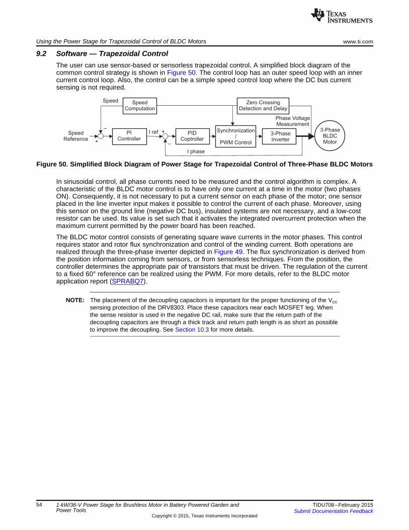
Speed SpeedComputation
Zero CrossingDetection and Delay
Phase VoltageMeasurement
3-PhaseInverter
Synchronization/
PWM Control
PIDCoptroller
PIController
SpeedReference +
–I ref
I phase
3-PhaseBLDCMotor
+
–
Using the Power Stage for Trapezoidal Control of BLDC Motors www.ti.com
9.2 Software — Trapezoidal ControlThe user can use sensor-based or sensorless trapezoidal control. A simplified block diagram of thecommon control strategy is shown in Figure 50. The control loop has an outer speed loop with an innercurrent control loop. Also, the control can be a simple speed control loop where the DC bus currentsensing is not required.
Figure 50. Simplified Block Diagram of Power Stage for Trapezoidal Control of Three-Phase BLDC Motors
In sinusoidal control, all phase currents need to be measured and the control algorithm is complex. Acharacteristic of the BLDC motor control is to have only one current at a time in the motor (two phasesON). Consequently, it is not necessary to put a current sensor on each phase of the motor; one sensorplaced in the line inverter input makes it possible to control the current of each phase. Moreover, usingthis sensor on the ground line (negative DC bus), insulated systems are not necessary, and a low-costresistor can be used. Its value is set such that it activates the integrated overcurrent protection when themaximum current permitted by the power board has been reached.
The BLDC motor control consists of generating square wave currents in the motor phases. This controlrequires stator and rotor flux synchronization and control of the winding current. Both operations arerealized through the three-phase inverter depicted in Figure 49. The flux synchronization is derived fromthe position information coming from sensors, or from sensorless techniques. From the position, thecontroller determines the appropriate pair of transistors that must be driven. The regulation of the currentto a fixed 60° reference can be realized using the PWM. For more details, refer to the BLDC motorapplication report (SPRABQ7).
NOTE: The placement of the decoupling capacitors is important for the proper functioning of the VDS
sensing protection of the DRV8303. Place these capacitors near each MOSFET leg. Whenthe sense resistor is used in the negative DC rail, make sure that the return path of thedecoupling capacitors are through a thick track and return path length is as short as possibleto improve the decoupling. See Section 10.3 for more details.
54 1-kW/36-V Power Stage for Brushless Motor in Battery Powered Garden and TIDU708–February 2015Power Tools Submit Documentation Feedback
Copyright © 2015, Texas Instruments Incorporated
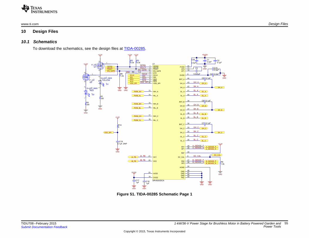
GND
OCTW
SCSVDD_SPI
EN_GATE
SDOSDO
SCS
GND
EN_GATE
FAULT
OCTW
GND
+3.3V+3.3V
+3.3V
VDD_SPI
1.0kR6
1.0R5
OCTW1
FAULT2
DTC3
SCS4
SDI5
SDO6
SCLK7
DC_CAL8
GVDD9
CP110
CP211
EN_GATE12
INH_A13
INL_A14
INH_B15
INL_B16
INH_C17
INL_C18
DVDD19
REF20
SO121
SO222
AVDD23
AGND24
PVDD25
SP226
SN227
SP128
SN129
SL_C30
GL_C31
SH_C32
GH_C33
BST_C34
SL_B35
GL_B36
SH_B37
GH_B38
BST_B39
SL_A40
GL_A41
SH_A42
GH_A43
BST_A44
VDD_SPI45
GND46
GND47
GND48
PAD49
U1
DRV8303DCA
SCLKSCLK
SDISDI
PWM_BH
PWM_BL
PWM_CH
PWM_CL
PWM_AH
PWM_AL
IA_FB
IB_FBIB_FB
IA_FB
1µFC16
GND
DVDD
1µFC17
GND
GND GND
B_ISENSE_N
B_ISENSE_P
DC_CALDC_CAL
GND
1.0kR9
+3.3V
A_ISENSE_P
A_ISENSE_N
SL_CSL_C
GL_CGL_C
GH_CGH_C
SH_CSH_C
0.1µFC7
GH_B
GL_B
SL_B
SH_B
GH_B
GL_B
SL_B
SH_B
0.1µFC6
GH_A
GL_A
SL_A
SH_A
GH_A
GL_A
SL_A
SH_A
0.1µFC5 GND
2.2µFC40.022µF
C3
+PVDD
GND
0.1µFC2
2.2µFC1
C1
A2
RED
D2
D-LED_0805
G1
S2
D3
P_CHQ2
GND
330R4
C1
A2
YELLOW
D1
D-LED_0805
GND
330R1
G1
S2
D3
P_CHQ1
+3.3V
+3.3V
GND
VDD_SPI
0R14
0.1µF, DNP
C19
FAULT
2.2µF
C39
2.2µFC15
3.3kR2
3.3kR3
A_ISENSE_PA_ISENSE_N
B_ISENSE_PB_ISENSE_N
www.ti.com Design Files
10 Design Files
10.1 SchematicsTo download the schematics, see the design files at TIDA-00285.
Figure 51. TIDA-00285 Schematic Page 1
55TIDU708–February 2015 1-kW/36-V Power Stage for Brushless Motor in Battery Powered Garden andPower ToolsSubmit Documentation Feedback
Copyright © 2015, Texas Instruments Incorporated
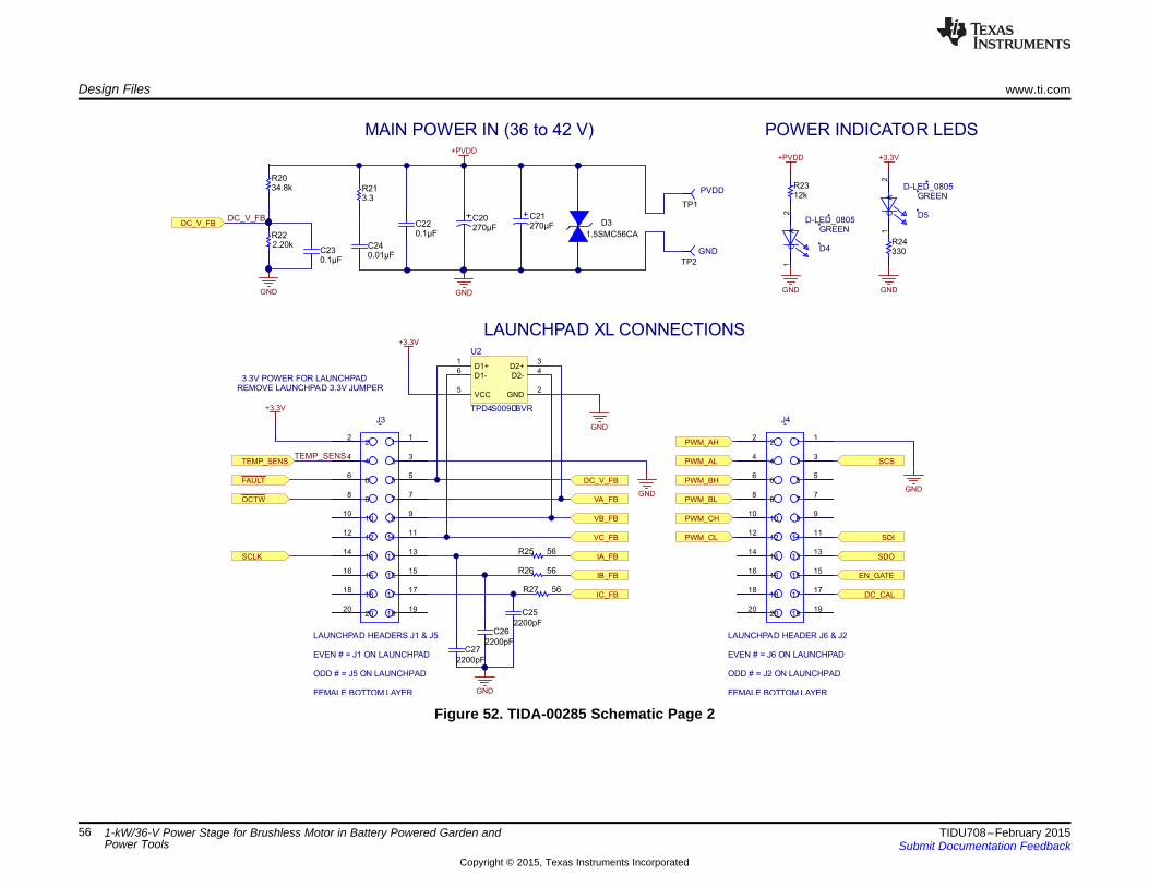
POWER INDICATOR LEDS
C1
A2
GREEN
D4
D-LED_0805
C1
A2
GREEN
D5
D-LED_0805
+PVDD +3.3V
GND GND
330R24
12kR23
3.3V POWER FOR LAUNCHPAD
LAUNCHPAD XL CONNECTIONS
LAUNCHPAD HEADERS J1 & J5
EVEN # = J1 ON LAUNCHPAD
ODD # = J5 ON LAUNCHPAD
FEMALE BOTTOM LAYER
11
22
33
44
55
66
77
88
99
1010
1111
1212
1313
1414
1515
1616
1717
1818
1919
2020
J3
+3.3V
FAULT
SCLK
GND
IA_FB
IB_FB
VA_FB
VB_FB
VC_FB
LAUNCHPAD HEADER J6 & J2
EVEN # = J6 ON LAUNCHPAD
ODD # = J2 ON LAUNCHPAD
FEMALE BOTTOM LAYER
11
22
33
44
55
66
77
88
99
1010
1111
1212
1313
1414
1515
1616
1717
1818
1919
2020
J4
PWM_AH
PWM_AL
PWM_BH
PWM_BL
PWM_CH
PWM_CL
SCS
GND
SDO
SDI
IC_FB
GND
56R25
56R26
56R27
2200pF
C272200pF
C262200pF
C25
OCTW
DC_V_FB
EN_GATE
DC_CAL
REMOVE LAUNCHPAD 3.3V JUMPER
TEMP_SENSTEMP_SENS
D1+1
GND2
D2+3
D2-4
VCC5
D1-6
U2
TPD4S009DBVR
GND
+3.3V
MAIN POWER IN (36 to 42 V)
DC_V_FB
+PVDD
GNDGND
34.8kR20
0.1µFC23
3.3R21
0.01µFC24
0.1µFC22
DC_V_FB
2.20kR22
TP1
TP2
270µFC20
D3
1.5SMC56CA
PVDD
GND
270µFC21
Design Files www.ti.com
Figure 52. TIDA-00285 Schematic Page 2
56 1-kW/36-V Power Stage for Brushless Motor in Battery Powered Garden and TIDU708–February 2015Power Tools Submit Documentation Feedback
Copyright © 2015, Texas Instruments Incorporated
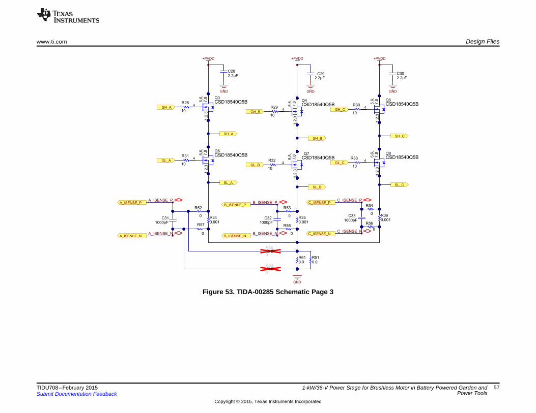
+PVDD +PVDD +PVDD
GH_A
GL_A
GH_B
GL_B
GH_C
GL_C
SH_A
SH_BSH_C
SL_A
SL_BSL_C
A_ISENSE_N
A_ISENSE_PB_ISENSE_P
B_ISENSE_N
GND GND GND
C_ISENSE_P
C_ISENSE_N
2.2µFC28
2.2µFC29
2.2µFC30
1000pFC31
1000pFC32
1000pFC33
10
R28
10
R31
10
R29
10
R32
10
R30
10
R33
0.001R36
0.001R34
0.001R350
R52
0
R57
0
R54
0
R56
0
R53
0
R55
4
7,8
1,2
,3
5,6
,
Q3CSD18540Q5B
4
7,8
1,2
,3
5,6
,
Q8CSD18540Q5B
4
7,8
1,2
,3
5,6
, Q4CSD18540Q5B
4
7,8
1,2
,3
5,6
,
Q6CSD18540Q5B
4
7,8
1,2
,3
5,6
, Q7CSD18540Q5B
4
7,8
1,2
,3
5,6
,
Q5CSD18540Q5B
GND
0.0R61
0.0R51
0
R58DNP
0
R59DNP
C_ISENSE_N
C_ISENSE_P
B_ISENSE_N
B_ISENSE_PA_ISENSE_P
A_ISENSE_N
www.ti.com Design Files
Figure 53. TIDA-00285 Schematic Page 3
57TIDU708–February 2015 1-kW/36-V Power Stage for Brushless Motor in Battery Powered Garden andPower ToolsSubmit Documentation Feedback
Copyright © 2015, Texas Instruments Incorporated
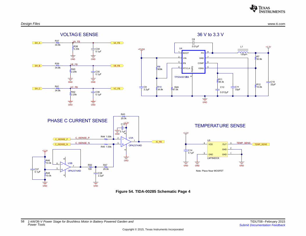
GND
+3.3V
GND
IC_FB
PHASE C CURRENT SENSE
C_ISENSE_P
C_ISENSE_N
10.0kR48
10.0kR46
+3.3V
GND
2.2µFC38
0.1µFC37
1.00kR44
1.00kR45
0.1µF
C13
GND
100
R50
1
3
2
48
U3A
OPA2374AID
7
5
6
48
U3B
OPA2374AID
SH_A VA_FB
SH_B VB_FB
SH_C VC_FB
GND GND
GND GND
GND GND
VC_FB
VB_FB
VA_FB
VOLTAG E SENSE
34.8k
R37
34.8k
R39
34.8k
R41
0.1µFC34
0.1µFC35
0.1µFC36
2.20kR38
2.20kR40
2.20kR42
BOOT1
VIN2
EN3
RT/CLK4
VSNS5
COMP6
GND7
PH8
PW
PD
9
U4
TPS54061DRB
2.2µFC9
22µFC10
97.6kR49
38.3kR11
0.012µF
C1233pFC11
30.9kR7
10.0kR12
120µH
L1+PVDD
+3.3V
GND
36 V to 3.3 V
GND1
GND2
OUT3
VDD4
GND5
U5
LMT84DCK
0.1µFC14
TEMP_SENSTEMP_SENS
GNDGNDGND
Note: Place Near MOSFET
+3.3V
TEMPERATURE SENSE
20.0k
R43
20.0k
R47
0.01µF
C8
C_ISENSE_P
C_ISENSE_N
34.8kR10
909kR8
Design Files www.ti.com
Figure 54. TIDA-00285 Schematic Page 4
space
58 1-kW/36-V Power Stage for Brushless Motor in Battery Powered Garden and TIDU708–February 2015Power Tools Submit Documentation Feedback
Copyright © 2015, Texas Instruments Incorporated
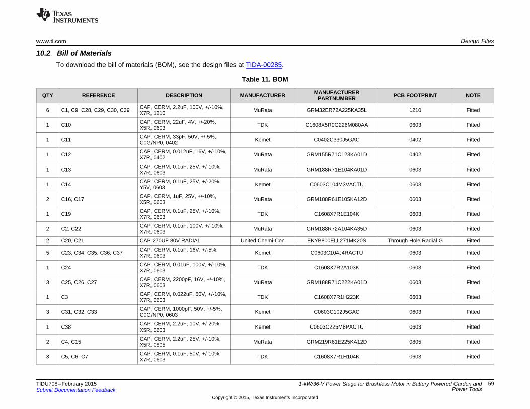
www.ti.com Design Files
10.2 Bill of MaterialsTo download the bill of materials (BOM), see the design files at TIDA-00285.
Table 11. BOM
MANUFACTURERQTY REFERENCE DESCRIPTION MANUFACTURER PCB FOOTPRINT NOTEPARTNUMBERCAP, CERM, 2.2uF, 100V, +/-10%,6 C1, C9, C28, C29, C30, C39 MuRata GRM32ER72A225KA35L 1210 FittedX7R, 1210CAP, CERM, 22uF, 4V, +/-20%,1 C10 TDK C1608X5R0G226M080AA 0603 FittedX5R, 0603CAP, CERM, 33pF, 50V, +/-5%,1 C11 Kemet C0402C330J5GAC 0402 FittedC0G/NP0, 0402CAP, CERM, 0.012uF, 16V, +/-10%,1 C12 MuRata GRM155R71C123KA01D 0402 FittedX7R, 0402CAP, CERM, 0.1uF, 25V, +/-10%,1 C13 MuRata GRM188R71E104KA01D 0603 FittedX7R, 0603CAP, CERM, 0.1uF, 25V, +/-20%,1 C14 Kemet C0603C104M3VACTU 0603 FittedY5V, 0603CAP, CERM, 1uF, 25V, +/-10%,2 C16, C17 MuRata GRM188R61E105KA12D 0603 FittedX5R, 0603CAP, CERM, 0.1uF, 25V, +/-10%,1 C19 TDK C1608X7R1E104K 0603 FittedX7R, 0603CAP, CERM, 0.1uF, 100V, +/-10%,2 C2, C22 MuRata GRM188R72A104KA35D 0603 FittedX7R, 0603
2 C20, C21 CAP 270UF 80V RADIAL United Chemi-Con EKYB800ELL271MK20S Through Hole Radial G FittedCAP, CERM, 0.1uF, 16V, +/-5%,5 C23, C34, C35, C36, C37 Kemet C0603C104J4RACTU 0603 FittedX7R, 0603CAP, CERM, 0.01uF, 100V, +/-10%,1 C24 TDK C1608X7R2A103K 0603 FittedX7R, 0603CAP, CERM, 2200pF, 16V, +/-10%,3 C25, C26, C27 MuRata GRM188R71C222KA01D 0603 FittedX7R, 0603CAP, CERM, 0.022uF, 50V, +/-10%,1 C3 TDK C1608X7R1H223K 0603 FittedX7R, 0603CAP, CERM, 1000pF, 50V, +/-5%,3 C31, C32, C33 Kemet C0603C102J5GAC 0603 FittedC0G/NP0, 0603CAP, CERM, 2.2uF, 10V, +/-20%,1 C38 Kemet C0603C225M8PACTU 0603 FittedX5R, 0603CAP, CERM, 2.2uF, 25V, +/-10%,2 C4, C15 MuRata GRM219R61E225KA12D 0805 FittedX5R, 0805CAP, CERM, 0.1uF, 50V, +/-10%,3 C5, C6, C7 TDK C1608X7R1H104K 0603 FittedX7R, 0603
59TIDU708–February 2015 1-kW/36-V Power Stage for Brushless Motor in Battery Powered Garden andPower ToolsSubmit Documentation Feedback
Copyright © 2015, Texas Instruments Incorporated
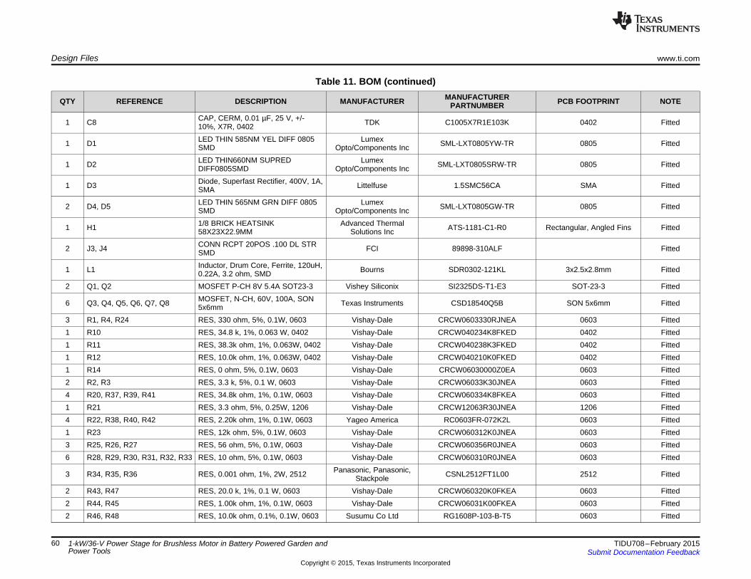
Design Files www.ti.com
Table 11. BOM (continued)MANUFACTURERQTY REFERENCE DESCRIPTION MANUFACTURER PCB FOOTPRINT NOTEPARTNUMBER
CAP, CERM, 0.01 µF, 25 V, +/-1 C8 TDK C1005X7R1E103K 0402 Fitted10%, X7R, 0402LED THIN 585NM YEL DIFF 0805 Lumex1 D1 SML-LXT0805YW-TR 0805 FittedSMD Opto/Components IncLED THIN660NM SUPRED Lumex1 D2 SML-LXT0805SRW-TR 0805 FittedDIFF0805SMD Opto/Components IncDiode, Superfast Rectifier, 400V, 1A,1 D3 Littelfuse 1.5SMC56CA SMA FittedSMALED THIN 565NM GRN DIFF 0805 Lumex2 D4, D5 SML-LXT0805GW-TR 0805 FittedSMD Opto/Components Inc1/8 BRICK HEATSINK Advanced Thermal1 H1 ATS-1181-C1-R0 Rectangular, Angled Fins Fitted58X23X22.9MM Solutions IncCONN RCPT 20POS .100 DL STR2 J3, J4 FCI 89898-310ALF FittedSMDInductor, Drum Core, Ferrite, 120uH,1 L1 Bourns SDR0302-121KL 3x2.5x2.8mm Fitted0.22A, 3.2 ohm, SMD
2 Q1, Q2 MOSFET P-CH 8V 5.4A SOT23-3 Vishey Siliconix SI2325DS-T1-E3 SOT-23-3 FittedMOSFET, N-CH, 60V, 100A, SON6 Q3, Q4, Q5, Q6, Q7, Q8 Texas Instruments CSD18540Q5B SON 5x6mm Fitted5x6mm
3 R1, R4, R24 RES, 330 ohm, 5%, 0.1W, 0603 Vishay-Dale CRCW0603330RJNEA 0603 Fitted1 R10 RES, 34.8 k, 1%, 0.063 W, 0402 Vishay-Dale CRCW040234K8FKED 0402 Fitted1 R11 RES, 38.3k ohm, 1%, 0.063W, 0402 Vishay-Dale CRCW040238K3FKED 0402 Fitted1 R12 RES, 10.0k ohm, 1%, 0.063W, 0402 Vishay-Dale CRCW040210K0FKED 0402 Fitted1 R14 RES, 0 ohm, 5%, 0.1W, 0603 Vishay-Dale CRCW06030000Z0EA 0603 Fitted2 R2, R3 RES, 3.3 k, 5%, 0.1 W, 0603 Vishay-Dale CRCW06033K30JNEA 0603 Fitted4 R20, R37, R39, R41 RES, 34.8k ohm, 1%, 0.1W, 0603 Vishay-Dale CRCW060334K8FKEA 0603 Fitted1 R21 RES, 3.3 ohm, 5%, 0.25W, 1206 Vishay-Dale CRCW12063R30JNEA 1206 Fitted4 R22, R38, R40, R42 RES, 2.20k ohm, 1%, 0.1W, 0603 Yageo America RC0603FR-072K2L 0603 Fitted1 R23 RES, 12k ohm, 5%, 0.1W, 0603 Vishay-Dale CRCW060312K0JNEA 0603 Fitted3 R25, R26, R27 RES, 56 ohm, 5%, 0.1W, 0603 Vishay-Dale CRCW060356R0JNEA 0603 Fitted6 R28, R29, R30, R31, R32, R33 RES, 10 ohm, 5%, 0.1W, 0603 Vishay-Dale CRCW060310R0JNEA 0603 Fitted
Panasonic, Panasonic,3 R34, R35, R36 RES, 0.001 ohm, 1%, 2W, 2512 CSNL2512FT1L00 2512 FittedStackpole2 R43, R47 RES, 20.0 k, 1%, 0.1 W, 0603 Vishay-Dale CRCW060320K0FKEA 0603 Fitted2 R44, R45 RES, 1.00k ohm, 1%, 0.1W, 0603 Vishay-Dale CRCW06031K00FKEA 0603 Fitted2 R46, R48 RES, 10.0k ohm, 0.1%, 0.1W, 0603 Susumu Co Ltd RG1608P-103-B-T5 0603 Fitted
60 1-kW/36-V Power Stage for Brushless Motor in Battery Powered Garden and TIDU708–February 2015Power Tools Submit Documentation Feedback
Copyright © 2015, Texas Instruments Incorporated
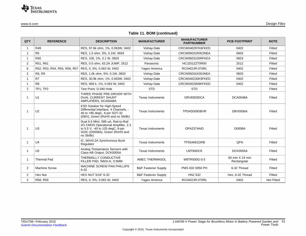
www.ti.com Design Files
Table 11. BOM (continued)MANUFACTURERQTY REFERENCE DESCRIPTION MANUFACTURER PCB FOOTPRINT NOTEPARTNUMBER
1 R49 RES, 97.6k ohm, 1%, 0.063W, 0402 Vishay-Dale CRCW040297K6FKED 0402 Fitted1 R5 RES, 1.0 ohm, 5%, 0.1W, 0603 Vishay-Dale CRCW06031R00JNEA 0603 Fitted1 R50 RES, 100, 1%, 0.1 W, 0603 Vishay-Dale CRCW0603100RFKEA 0603 Fitted2 R51, R61 RES, 0.0 ohm, 63.2A JUMP, 2512 Panasonic HCJ2512ZT0R00 2512 Fitted6 R52, R53, R54, R55, R56, R57 RES, 0, 5%, 0.063 W, 0402 Yageo America RC0402JR-070RL 0402 Fitted2 R6, R9 RES, 1.0k ohm, 5%, 0.1W, 0603 Vishay-Dale CRCW06031K00JNEA 0603 Fitted1 R7 RES, 30.9k ohm, 1%, 0.063W, 0402 Vishay-Dale CRCW040230K9FKED 0402 Fitted1 R8 RES, 909 k, 1%, 0.063 W, 0402 Vishay-Dale CRCW0402909KFKED 0402 Fitted2 TP1, TP2 Test Point, O.040 Hole STD STD Fitted
THREE PHASE PRE-DRIVER WITH1 U1 DUAL CURRENT SHUNT Texas Instruments DRV8303DCA DCA0048A Fitted
AMPLIFIERS, DCA0048AESD Solution for High-SpeedDifferential Interface, 4 Channels, -1 U2 Texas Instruments TPD4S009DBVR DBV0006A Fitted40 to +85 degC, 6-pin SOT-32(DBV), Green (RoHS and no Sb/Br)Dual 6.5 MHz, 585 uA, Rail-to-RailI/O CMOS Operational Amplifier, 2.3
1 U3 to 5.5 V, -40 to 125 degC, 8-pin Texas Instruments OPA2374AID D0008A FittedSOIC (D0008A), Green (RoHS andno Sb/Br)IC, 60V/0.2A Synchronous Buck1 U4 Texas Instruments TPS54061DRB QFN FittedRegulatorAnalog Temperature Sensors with1 U5 Texas Instruments LMT84DCK DCK0005A FittedClass-AB Output, DCK0005ATHERMALLY CONDUCTIVE 60 mm X 24 mm1 Thermal Pad AMEC THERMASOL W8TR500G-0.5 FittedFILLER PAD, 5W/m.K, 0.5MM RectangularMACHINE SCREW PAN PHILLIPS2 Machine Screw B&F Fastener Supply PMS 632 0050 PH 6-32 Thread Fitted6-32
2 Hex Nut HEX NUT 5/16" 6-32 B&F Fastener Supply HNZ 632 Hex, 6-32 Thread Fitted2 R58, R59 RES, 0, 5%, 0.063 W, 0402 Yageo America RC0402JR-070RL 0402 Not Fitted
61TIDU708–February 2015 1-kW/36-V Power Stage for Brushless Motor in Battery Powered Garden andPower ToolsSubmit Documentation Feedback
Copyright © 2015, Texas Instruments Incorporated
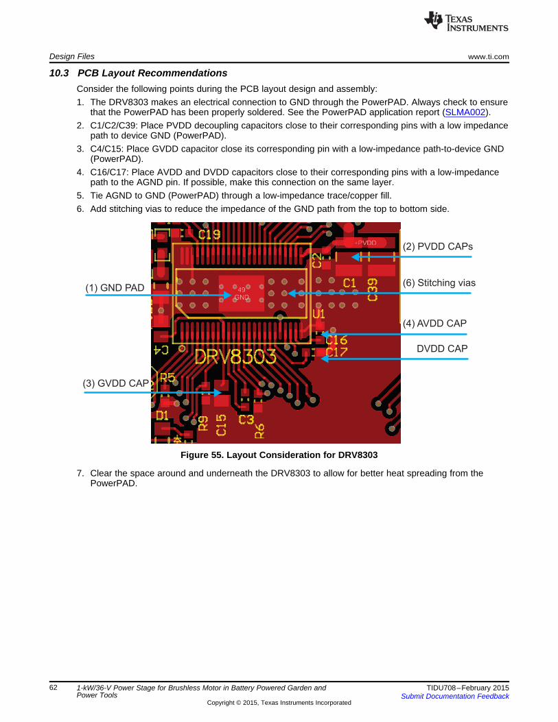
(1) GND PAD
(3) GVDD CAP
(2) PVDD CAPs
(6) Stitching vias
(4) AVDD CAP
(4) DVDD CAP
Design Files www.ti.com
10.3 PCB Layout RecommendationsConsider the following points during the PCB layout design and assembly:1. The DRV8303 makes an electrical connection to GND through the PowerPAD. Always check to ensure
that the PowerPAD has been properly soldered. See the PowerPAD application report (SLMA002).2. C1/C2/C39: Place PVDD decoupling capacitors close to their corresponding pins with a low impedance
path to device GND (PowerPAD).3. C4/C15: Place GVDD capacitor close its corresponding pin with a low-impedance path-to-device GND
(PowerPAD).4. C16/C17: Place AVDD and DVDD capacitors close to their corresponding pins with a low-impedance
path to the AGND pin. If possible, make this connection on the same layer.5. Tie AGND to GND (PowerPAD) through a low-impedance trace/copper fill.6. Add stitching vias to reduce the impedance of the GND path from the top to bottom side.
Figure 55. Layout Consideration for DRV8303
7. Clear the space around and underneath the DRV8303 to allow for better heat spreading from thePowerPAD.
62 1-kW/36-V Power Stage for Brushless Motor in Battery Powered Garden and TIDU708–February 2015Power Tools Submit Documentation Feedback
Copyright © 2015, Texas Instruments Incorporated
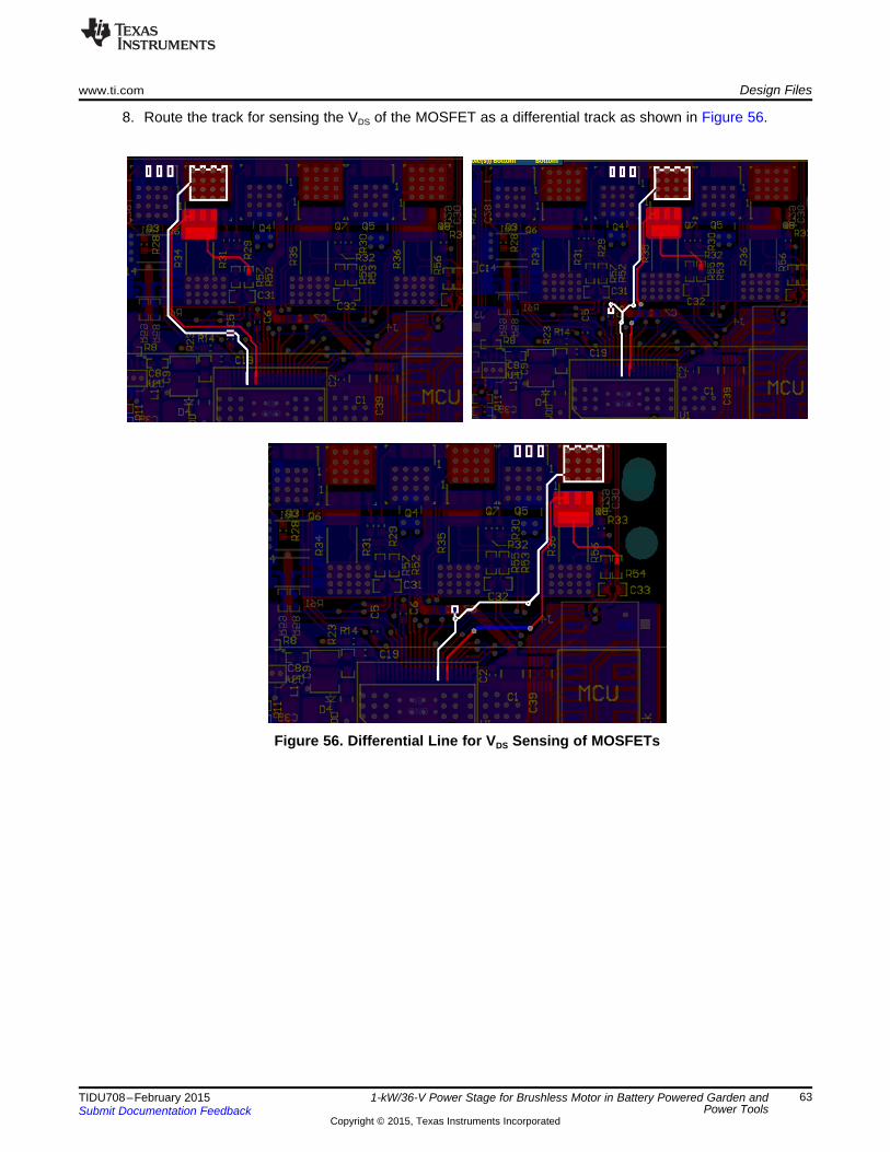
www.ti.com Design Files
8. Route the track for sensing the VDS of the MOSFET as a differential track as shown in Figure 56.
Figure 56. Differential Line for VDS Sensing of MOSFETs
63TIDU708–February 2015 1-kW/36-V Power Stage for Brushless Motor in Battery Powered Garden andPower ToolsSubmit Documentation Feedback
Copyright © 2015, Texas Instruments Incorporated

GND track in middle layer
PVDD track in middle layer
GND star point
3.3-V layer
Design Files www.ti.com
9. In the reference design, the PCB is made in four layer with 2-Oz (70 micron) copper thickness in everylayer. The power tracks are made wide to carry a high current. Figure 57 shows the current carryingtrack from the power input point. The tracks in different layers are connected by arrays of stitching vias.
Figure 57. Layout Considerations for Power Handling and GND Tracks
10. A GND star point is defined in the PCB from where the GND path for the DRV8303 and other signalcircuits in the board is tapped.
11. For better thermal dissipation from the MOSFET to the PCB, increase the copper area around theMOSFET pad as much as possible. Use arrays of vias under the drain pad of the MOSFET, which willhelp in better heat dissipation through the bottom surface copper area. Add a small heat sink or copperbars to the bottom surface of PCB to aid heat dissipation.
64 1-kW/36-V Power Stage for Brushless Motor in Battery Powered Garden and TIDU708–February 2015Power Tools Submit Documentation Feedback
Copyright © 2015, Texas Instruments Incorporated
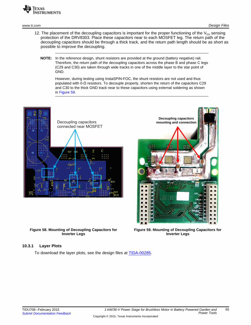
Decoupling capacitors mounting and connectionDecoupling capacitors
connected near MOSFET
www.ti.com Design Files
12. The placement of the decoupling capacitors is important for the proper functioning of the VDS sensingprotection of the DRV8303. Place these capacitors near to each MOSFET leg. The return path of thedecoupling capacitors should be through a thick track, and the return path length should be as short aspossible to improve the decoupling.
NOTE: In the reference design, shunt resistors are provided at the ground (battery negative) rail.Therefore, the return path of the decoupling capacitors across the phase B and phase C legs(C29 and C30) are taken through wide tracks in one of the middle layer to the star point ofGND.
However, during testing using InstaSPIN-FOC, the shunt resistors are not used and thuspopulated with 0-Ω resistors. To decouple properly, shorten the return of the capacitors C29and C30 to the thick GND track near to these capacitors using external soldering as shownin Figure 59.
Figure 58. Mounting of Decoupling Capacitors for Figure 59. Mounting of Decoupling Capacitors forInverter Legs Inverter Legs
10.3.1 Layer PlotsTo download the layer plots, see the design files at TIDA-00285.
65TIDU708–February 2015 1-kW/36-V Power Stage for Brushless Motor in Battery Powered Garden andPower ToolsSubmit Documentation Feedback
Copyright © 2015, Texas Instruments Incorporated
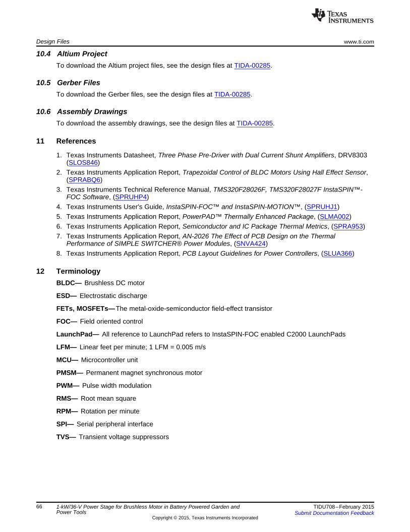
Design Files www.ti.com
10.4 Altium ProjectTo download the Altium project files, see the design files at TIDA-00285.
10.5 Gerber FilesTo download the Gerber files, see the design files at TIDA-00285.
10.6 Assembly DrawingsTo download the assembly drawings, see the design files at TIDA-00285.
11 References
1. Texas Instruments Datasheet, Three Phase Pre-Driver with Dual Current Shunt Amplifiers, DRV8303(SLOS846)
2. Texas Instruments Application Report, Trapezoidal Control of BLDC Motors Using Hall Effect Sensor,(SPRABQ6)
3. Texas Instruments Technical Reference Manual, TMS320F28026F, TMS320F28027F InstaSPIN™-FOC Software, (SPRUHP4)
4. Texas Instruments User's Guide, InstaSPIN-FOC™ and InstaSPIN-MOTION™, (SPRUHJ1)5. Texas Instruments Application Report, PowerPAD™ Thermally Enhanced Package, (SLMA002)6. Texas Instruments Application Report, Semiconductor and IC Package Thermal Metrics, (SPRA953)7. Texas Instruments Application Report, AN-2026 The Effect of PCB Design on the Thermal
Performance of SIMPLE SWITCHER® Power Modules, (SNVA424)8. Texas Instruments Application Report, PCB Layout Guidelines for Power Controllers, (SLUA366)
12 TerminologyBLDC— Brushless DC motor
ESD— Electrostatic discharge
FETs, MOSFETs—The metal-oxide-semiconductor field-effect transistor
FOC— Field oriented control
LaunchPad— All reference to LaunchPad refers to InstaSPIN-FOC enabled C2000 LaunchPads
LFM— Linear feet per minute; 1 LFM = 0.005 m/s
MCU— Microcontroller unit
PMSM— Permanent magnet synchronous motor
PWM— Pulse width modulation
RMS— Root mean square
RPM— Rotation per minute
SPI— Serial peripheral interface
TVS— Transient voltage suppressors
66 1-kW/36-V Power Stage for Brushless Motor in Battery Powered Garden and TIDU708–February 2015Power Tools Submit Documentation Feedback
Copyright © 2015, Texas Instruments Incorporated

www.ti.com About the Author
13 About the AuthorNELSON ALEXANDER is a systems engineer at Texas Instruments where he is responsible fordeveloping subsystem design solutions for the Industrial Motor Drive segment. Nelson has been with TIsince 2011 and has been involved in designing products related to smart grid and embedded systemsbased on microcontrollers. Nelson earned his bachelor of technology in electrical engineering at MSRIT,Bangalore.
MANU BALAKRISHNAN is a systems engineer at Texas Instruments where he is responsible fordeveloping subsystem design solutions for the Industrial Motor Drive segment. Manu brings to this role hisexperience in power electronics, analog, and mixed signal designs. He has system-level product designexperience in permanent magnet motor drives. Manu earned his bachelor of technology in electrical andelectronics engineering from the University of Kerala and his master of technology in power electronicsfrom National Institute of Technology Calicut, India.
N. NAVANEETH KUMAR is a systems architect at Texas Instruments where he is responsible fordeveloping subsystem solutions for motor controls within Industrial Systems. N. Navaneeth brings to thisrole his extensive experience in power electronics, EMC, analog, and mixed signal designs. He hassystem-level product design experience in drives, solar inverters, UPS, and protection relays. N.Navaneeth earned his bachelor of electronics and communication engineering from Bharathiar University,India and his master of science in electronic product development from Bolton University, UK.
67TIDU708–February 2015 1-kW/36-V Power Stage for Brushless Motor in Battery Powered Garden andPower ToolsSubmit Documentation Feedback
Copyright © 2015, Texas Instruments Incorporated

IMPORTANT NOTICE FOR TI REFERENCE DESIGNS
Texas Instruments Incorporated ("TI") reference designs are solely intended to assist designers (“Buyers”) who are developing systems thatincorporate TI semiconductor products (also referred to herein as “components”). Buyer understands and agrees that Buyer remainsresponsible for using its independent analysis, evaluation and judgment in designing Buyer’s systems and products.TI reference designs have been created using standard laboratory conditions and engineering practices. TI has not conducted anytesting other than that specifically described in the published documentation for a particular reference design. TI may makecorrections, enhancements, improvements and other changes to its reference designs.Buyers are authorized to use TI reference designs with the TI component(s) identified in each particular reference design and to modify thereference design in the development of their end products. HOWEVER, NO OTHER LICENSE, EXPRESS OR IMPLIED, BY ESTOPPELOR OTHERWISE TO ANY OTHER TI INTELLECTUAL PROPERTY RIGHT, AND NO LICENSE TO ANY THIRD PARTY TECHNOLOGYOR INTELLECTUAL PROPERTY RIGHT, IS GRANTED HEREIN, including but not limited to any patent right, copyright, mask work right,or other intellectual property right relating to any combination, machine, or process in which TI components or services are used.Information published by TI regarding third-party products or services does not constitute a license to use such products or services, or awarranty or endorsement thereof. Use of such information may require a license from a third party under the patents or other intellectualproperty of the third party, or a license from TI under the patents or other intellectual property of TI.TI REFERENCE DESIGNS ARE PROVIDED "AS IS". TI MAKES NO WARRANTIES OR REPRESENTATIONS WITH REGARD TO THEREFERENCE DESIGNS OR USE OF THE REFERENCE DESIGNS, EXPRESS, IMPLIED OR STATUTORY, INCLUDING ACCURACY ORCOMPLETENESS. TI DISCLAIMS ANY WARRANTY OF TITLE AND ANY IMPLIED WARRANTIES OF MERCHANTABILITY, FITNESSFOR A PARTICULAR PURPOSE, QUIET ENJOYMENT, QUIET POSSESSION, AND NON-INFRINGEMENT OF ANY THIRD PARTYINTELLECTUAL PROPERTY RIGHTS WITH REGARD TO TI REFERENCE DESIGNS OR USE THEREOF. TI SHALL NOT BE LIABLEFOR AND SHALL NOT DEFEND OR INDEMNIFY BUYERS AGAINST ANY THIRD PARTY INFRINGEMENT CLAIM THAT RELATES TOOR IS BASED ON A COMBINATION OF COMPONENTS PROVIDED IN A TI REFERENCE DESIGN. IN NO EVENT SHALL TI BELIABLE FOR ANY ACTUAL, SPECIAL, INCIDENTAL, CONSEQUENTIAL OR INDIRECT DAMAGES, HOWEVER CAUSED, ON ANYTHEORY OF LIABILITY AND WHETHER OR NOT TI HAS BEEN ADVISED OF THE POSSIBILITY OF SUCH DAMAGES, ARISING INANY WAY OUT OF TI REFERENCE DESIGNS OR BUYER’S USE OF TI REFERENCE DESIGNS.TI reserves the right to make corrections, enhancements, improvements and other changes to its semiconductor products and services perJESD46, latest issue, and to discontinue any product or service per JESD48, latest issue. Buyers should obtain the latest relevantinformation before placing orders and should verify that such information is current and complete. All semiconductor products are soldsubject to TI’s terms and conditions of sale supplied at the time of order acknowledgment.TI warrants performance of its components to the specifications applicable at the time of sale, in accordance with the warranty in TI’s termsand conditions of sale of semiconductor products. Testing and other quality control techniques for TI components are used to the extent TIdeems necessary to support this warranty. Except where mandated by applicable law, testing of all parameters of each component is notnecessarily performed.TI assumes no liability for applications assistance or the design of Buyers’ products. Buyers are responsible for their products andapplications using TI components. To minimize the risks associated with Buyers’ products and applications, Buyers should provideadequate design and operating safeguards.Reproduction of significant portions of TI information in TI data books, data sheets or reference designs is permissible only if reproduction iswithout alteration and is accompanied by all associated warranties, conditions, limitations, and notices. TI is not responsible or liable forsuch altered documentation. Information of third parties may be subject to additional restrictions.Buyer acknowledges and agrees that it is solely responsible for compliance with all legal, regulatory and safety-related requirementsconcerning its products, and any use of TI components in its applications, notwithstanding any applications-related information or supportthat may be provided by TI. Buyer represents and agrees that it has all the necessary expertise to create and implement safeguards thatanticipate dangerous failures, monitor failures and their consequences, lessen the likelihood of dangerous failures and take appropriateremedial actions. Buyer will fully indemnify TI and its representatives against any damages arising out of the use of any TI components inBuyer’s safety-critical applications.In some cases, TI components may be promoted specifically to facilitate safety-related applications. With such components, TI’s goal is tohelp enable customers to design and create their own end-product solutions that meet applicable functional safety standards andrequirements. Nonetheless, such components are subject to these terms.No TI components are authorized for use in FDA Class III (or similar life-critical medical equipment) unless authorized officers of the partieshave executed an agreement specifically governing such use.Only those TI components that TI has specifically designated as military grade or “enhanced plastic” are designed and intended for use inmilitary/aerospace applications or environments. Buyer acknowledges and agrees that any military or aerospace use of TI components thathave not been so designated is solely at Buyer's risk, and Buyer is solely responsible for compliance with all legal and regulatoryrequirements in connection with such use.TI has specifically designated certain components as meeting ISO/TS16949 requirements, mainly for automotive use. In any case of use ofnon-designated products, TI will not be responsible for any failure to meet ISO/TS16949.IMPORTANT NOTICE
Mailing Address: Texas Instruments, Post Office Box 655303, Dallas, Texas 75265Copyright © 2015, Texas Instruments Incorporated