1 introduction - ieesa · · 2001-04-04introduction 1 1 – 3 figure 1.2 adsp-2106x sharc block...
TRANSCRIPT

1Introduction
1 – 3
Figure 1.2 ADSP-2106x SHARC Block Diagram
This user’s manual contains architectural information and aninstruction set description required for the design and programming ofADSP-2106x-based systems. In addition to this manual, hardwaredesigners should refer to the ADSP-21060/62 Data Sheet and theADSP-21061 Data Sheet for timing, electrical, and packagespecifications.
AAAAAAAAAAAAAAAAAAAAAAAAAAAA
PM Address Bus (PMA) 24
DM Address Bus (DMA) 32
PM Data Bus (PMD)
DM Data Bus (DMD)
AAAAAA AAAAAA
AAAAAAAAAAAAAAAAAAAAAAAAAAAAAA
PROCESSOR PORT I/O PORT
SERIAL PORTS (2)
LINK PORTS (6)
INSTRUCTIONCACHE
32 x 48-Bit
DAG 28 x 4 x 24
DAG 18 x 4 x 32
TIMER
DMA CONTROLLER
Addr Bus Mux
32
48
AAAAAAAAAAAAAAAAAAAAAAAA
IOPREGISTERS
Control,Status, &
Data Buffers
6
6
36
4AAAAAAAAAAAAAAAAAAAAAAAAAAAAAAA
AAAAAAAAAAAAAAAAAAAAAAA
AA
ADDR DATA ADDR DATA
AA
7
A
A
JTAG
Bus Connect
(PX)
MULTIPLIER BARREL SHIFTER
ALU
AAAAAAAA
AAAAAAA
DATAREGISTER
FILE
16 x 40-Bit
AAAAAACore Processor
AAAAAAAAAADual-Ported SRAM
Two Independent,Dual-Ported Blocks
BL
OC
K 0
BL
OC
K 1
AAAAAAAAAAExternal Port
HOST INTERFACE
Test &Emulation
PROGRAMSEQUENCER
MULTIPROCESSORINTERFACE
48
IOD48
IOA17
AAAAAAAAA
IOD
EP
D
DM
D
PM
D
EP
A
IOA
AAAAAI/O Processor
AAAAAAA32/40
PMA
EPA
DMA
PMD
EPD
DMD
Data Bus Mux
AAAAAAAAAAAAA
*
* not available on the ADSP-21061
1 Introduction
1 – 4
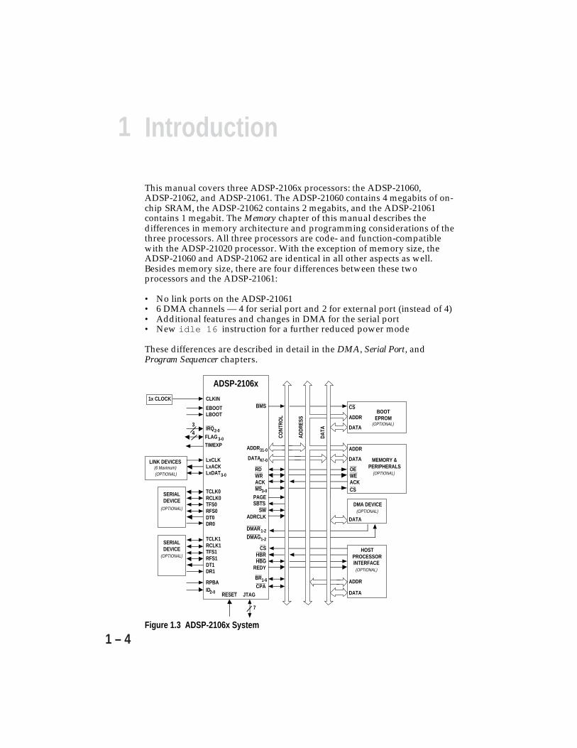
This manual covers three ADSP-2106x processors: the ADSP-21060, ADSP-21062, and ADSP-21061. The ADSP-21060 contains 4 megabits of on-chip SRAM, the ADSP-21062 contains 2 megabits, and the ADSP-21061contains 1 megabit. The Memory chapter of this manual describes thedifferences in memory architecture and programming considerations of thethree processors. All three processors are code- and function-compatiblewith the ADSP-21020 processor. With the exception of memory size, theADSP-21060 and ADSP-21062 are identical in all other aspects as well.Besides memory size, there are four differences between these twoprocessors and the ADSP-21061:
• No link ports on the ADSP-21061• 6 DMA channels — 4 for serial port and 2 for external port (instead of 4)• Additional features and changes in DMA for the serial port• New idle 16 instruction for a further reduced power mode
These differences are described in detail in the DMA, Serial Port, andProgram Sequencer chapters.
Figure 1.3 ADSP-2106x System
ADDR
DATA
BOOT EPROM
CLKIN
RESET
IRQ2-0
EBOOTLBOOT
FLAG 3-0
DMAR1-2DMAG1-2
LxCLKLxACKLxDAT3-0
TIMEXP
RPBAID2-0
BMS
ADSP-2106x
ADDR
DATA
DATA
ADDR
DATA
ADDR31-0
DATA47-0
CS
MEMORY & PERIPHERALS
DMA DEVICE
(OPTIONAL)
LINK DEVICES(6 Maximum)(OPTIONAL)
(OPTIONAL)
SERIALDEVICE
(OPTIONAL)
(OPTIONAL)
(OPTIONAL)
JTAG
ADDR
ESS
DATA
CONT
ROL
7
4
3
SERIALDEVICE
(OPTIONAL)
HOSTPROCESSORINTERFACE
BR1-6
1x CLOCK
CPA
OEWEACKCS
RDWRACKMS3-0
PAGESBTS
SWADRCLK
CSHBRHBG
REDY
TCLK1RCLK1TFS1RFS1DT1DR1
TCLK0RCLK0TFS0RFS0DT0DR0
44444Writing & AssemblingWriting & AssemblingWriting & AssemblingWriting & AssemblingWriting & AssemblingSource FilesSource FilesSource FilesSource FilesSource Files
4 – 54 – 54 – 54 – 54 – 5
3. tell the assembler to store floating-point data with 40-bit precision
4. tell the assembler to round a floating-point value to zero if it does notfit in the 40-bit format.
The initial directives are followed by one or more segments. A segmentbegins with a .SEGMENT directive and ends with a .ENDSEGdirective. Four segments are shown in Figure 4.2. The first segmentcontains data memory data. In this segment, variables and buffers aredeclared and can be initialized. The next segment contains I/O portsmapped to program memory. Each port has a unique name by which itcan be identified for reading and writing. The last two segmentscontain code—primarily instructions but also possibly more directives,such as for conditional assembly.
Individual lines in a source file must be no more than 200 characters inlength. Program labels are placed at the start of a line and followed bya colon:
startup: AY0=2; {beginning of program}
4.2 .24 .2 .24 .2 .24 .2 .24 .2 .2 Symbols & KeywordsSymbols & KeywordsSymbols & KeywordsSymbols & KeywordsSymbols & KeywordsA symbol is a character string used in one of two ways. Symbols whichyou define in assembly language code are used to represent somethingsuch as an address or data value. Other symbols are reservedkeywords recognized by the assembler.
A user-defined symbol in an assembly source file can be a datavariable, data buffer, program label, macro or constant.
Symbols consist of one character from the set:
• Uppercase letters “ A ” through “ Z ”• Lowercase letters “ a ” through “ z ”• The underscore character “ _ ”
followed by any sequence of characters from the set:
• Uppercase letters “ A ” through “ Z ”• Lowercase letters “ a ” through “ z ”• The underscore character “ _ ”• Digits “ 0 ” through “ 9 ”

44444 Writing & AssemblingWriting & AssemblingWriting & AssemblingWriting & AssemblingWriting & AssemblingSource FilesSource FilesSource FilesSource FilesSource Files
4 – 64 – 64 – 64 – 64 – 6
In other words, your symbols may not start with a digit. A symbolmay be any length, except for segment names, which must be no morethan eight characters long. Here are some examples of typical symbolsand what they might name:
xoperand data variableinput_array data buffersubroutine1 program labelAD_INPUT memory-mapped port
Symbols may have any combination of uppercase and lowercaseletters. Symbol names are always case-sensitive; for example,AD_INPUT must always be referred to in uppercase letters, and thesymbol ad_input is treated as a different symbol.
A symbol must be unique only in its file. You can use the same symbolin another file and the linker will not confuse the two when it links thefiles together. If you do want a symbol used in several files torepresent one entity (address, variable, etc.), you must declare it to beglobal; see “Global Data Structures,” later in this chapter.
Table 4.1 lists the reserved assembler keywords. You may not use akeyword as a symbol in your code. Both the uppercase and lowercaseversions of keywords are reserved. The architecture description filealso uses keywords; they are listed in the Chapter 3, WritingTheArchitecture Description. Consult both of these tables beforechoosing symbol names.
4.2 .34 .2 .34 .2 .34 .2 .34 .2 .3 Assembler ExpressionsAssembler ExpressionsAssembler ExpressionsAssembler ExpressionsAssembler ExpressionsThe ADSP-21000 Family Assembler can evaluate expressions in sourcecode. An expression may be used wherever a numeric value isexpected.
Two kinds of expressions are allowed:
• an arithmetic or logical operation on two or more constants
examples: 2.9e-5 + 1.29 (128 – 48) / 3 0x55 & 0x0F

44444Writing & AssemblingWriting & AssemblingWriting & AssemblingWriting & AssemblingWriting & AssemblingSource FilesSource FilesSource FilesSource FilesSource Files
4 – 74 – 74 – 74 – 74 – 7
.BANK
.ENDSYS
.PROCESSOR
.SEGMENT
.SYSTEMABSACACTADSP21020ADSP_21020ANDASHIFTASTATAVB0B1B10B11B12B13B14B15B2B3B4B5B6B7B8B9BCLRBEGINBITBITREVBOTHBSETBTGLBTSTBYCACACHECALLCDFAULTCHCICLCLIPCLRCODECOMPCOPYSIGN
COSCURLCNTRDAB1DAB2DADDRDAI1DAI2DBDECDMDM0DM1DM2DM3DMA1EDMA1SDMA2EDMA2SDMADRDMAPARITYCKDMBANK1DMBANK2DMBANK3DMDATADMWAITDODOVLDRAMECEEITHERELSEEMOVERLAYEMUCLKENDENDSEGEQEXEXPEXP2EXTERNEXTERNALF0F1F10F11F12F13F14F15F2F3
F4F5F6F7F8F9FADDRFDEPFEXTFIXFLAG0_INFLAG1_INFLAG2_INFLAG3_INFLOATFMERGFOREVERFRFTAFTBFTCGEGLOBALGTHEAPI0I1I10I11I12I13I14I15I2I3I4I5I6I7I8I9IDLEIFIMASKIMASKPINCINTERNALIRPTLJUMPL0L1
L10L11L12L13L14L15L2L3L4L5L6L7L8L9LALADDRLCELCNTRLELEFTOLEFTZLOADLOG2LOGBLOOPLSHIFTLTM0M1M10M11M12M13M14M15M2M3M4M5M6M7M8M9MANTMAXMINMODMODE1MODE2MODIFYMR0B
MR0FMR1BMR1FMR2BMR2FMRBMRFMSMVNENEWPAGENOFONOFZNOPNORMALNOTNUORP20P24P32P40PACKPARITYCKPASSPCPCSTKPCSTKPPGFAULTPGMODEPGSIZEPGWAITPMPM0PM1PMADRPMBANK1PMDAEPMDASPMDATAPMWAITPOPPORTPOVL0POVL1PRECISIONPSA1EPSA1SPSA2EPSA2SPSA3E
PSA3SPSA4EPSA4SPUSHPXPX1PX2R0R1R10R11R12R13R14R15R2R3R4R5R6R7R8R9RAMREADRECIPSRNDROMROTROUND_MINUSROUND_NEARESTROUND_PLUSROUND_ZERORSRSQRTSRTIRTSSATSCALBSESEGMENTSETSFSHFSHPSISINSQRSRSRAMSSF
SSFRSSISSIRSTSTACKSTEPSTKYSTSSUFSUFRSUISUIRSVSZTCOUNTTFTGLTPERIODTRUETSTUFUIUNPACKUNTILURUSFUSFRUSIUSIRUSTAT1USTAT2UUFUUFRUUIUUIRVARWITHWTMODEWTSTATESXOR
Table 4.1 Assembler-Reserved KeywordsTable 4.1 Assembler-Reserved KeywordsTable 4.1 Assembler-Reserved KeywordsTable 4.1 Assembler-Reserved KeywordsTable 4.1 Assembler-Reserved Keywords
44444 Writing & AssemblingWriting & AssemblingWriting & AssemblingWriting & AssemblingWriting & AssemblingSource FilesSource FilesSource FilesSource FilesSource Files
4 – 84 – 84 – 84 – 84 – 8
Expressions may use the following operators, which are a subset ofthe operators recognized by the C programming language:
( ) left, right parenthesis~ – ones complement, unary minus* / % multiply, divide, modulus+ – addition, subtraction<< >> bitwise shifts& bitwise AND| bitwise OR^ bitwise XOR
These are listed in order of precedence.
• a symbol plus or minus an integer value
examples: data – 8 data_buffer + 15 startup + 2
The symbols above are either data variables, data buffers orprogram labels. They represent data or address values.
If any operand in an expression is a floating-point value, the value ofthe expression is stored in floating-point format.
4.2 .44 .2 .44 .2 .44 .2 .44 .2 .4 Buffer Length OperatorBuffer Length OperatorBuffer Length OperatorBuffer Length OperatorBuffer Length OperatorA special “length of” ( @ ) operator is recognized by the assembler. Thisoperator is used with symbols which name data buffers:
@buffer_name is evaluated as the length (number of words) of thebuffer
The buffer_name must be declared in the same file@buffer_name is used. Simple expressions may be created byadding or subtracting a constant from the operator term:
@buffer_name ± constant
Example: @array – 10
44444Writing & AssemblingWriting & AssemblingWriting & AssemblingWriting & AssemblingWriting & AssemblingSource FilesSource FilesSource FilesSource FilesSource Files
4 – 94 – 94 – 94 – 94 – 9
The @ operator can be used to load L (length) registers when settingup circular buffers; for example:
Data segment:.VAR real_data[n]; {n=number of input samples}
Code segment:B5=real_data; {buffer base address} {I5 loads automatically}L5=@real_data; {buffer length}M6=1; {post-modify I5 by 1}LCNTR=@real_data, DO loop UNTIL LCE;
{loop counter=bufferlength}
F0=DM(I5,M6); {get next sample}…
loop: …
This code fragment determines the base address and length of thecircular buffer real_data . The buffer length value contained in L5determines when addressing wraps around to the top of the buffer.Further information on circular buffers can be found in the ADSP-21020 User’s Manual and ADSP-2106x SHARC User’s Manual.
4.2 .54 .2 .54 .2 .54 .2 .54 .2 .5 C o m m e n t sC o m m e n t sC o m m e n t sC o m m e n t sC o m m e n t sIn working with the asm21k assembler, you will note several codingconventions common to C programming. These include the /* and*/ comment delimiters and the #include and #definedirectives. These conventions are allowed in asm21k and benefitboth the programmer and maintainer of your application by makingthe code more readable. On the other hand, the ; and ! commentdelimiters are not allowed here or in the C compiler. The followingtable summarizes the safe use of comment delimiters:
File Type Comment DelimiterAssembler Soure /* comment */C Compiler Source /* comment */Architecture (*.ach ) Files !commentInitialization (*.ini ) Files ;commentI/O Port Description (*.prt ) Files !comment

44444 Writing & AssemblingWriting & AssemblingWriting & AssemblingWriting & AssemblingWriting & AssemblingSource FilesSource FilesSource FilesSource FilesSource Files
4 – 104 – 104 – 104 – 104 – 10
4 . 34 . 34 . 34 . 34 . 3PREPROCESSOR DIRECTIVESPREPROCESSOR DIRECTIVESPREPROCESSOR DIRECTIVESPREPROCESSOR DIRECTIVESPREPROCESSOR DIRECTIVESThe ADSP-210x0 assembler includes a preprocessor which allows youto use the C-style directives listed in Table 4.2 in your assemblylanguage code. The preprocessor handles these directives as well asany related code (e.g., expansion of macros created with the #definedirective). The preprocessor is automatically run before the assemblerunless you use the assembler’s –sp (skip preprocessor) switch.Preprocessor directives must be lowercase, unlike the other assemblerdirectives which can be either uppercase or lowercase.
Note: Preprocessor directives must start at left margin. Do not useleading spaces before the # character.
Directive Function#define define a macro or constant#undef undo macro definition# if, #endif conditional assembly#else, #elif multiple conditional blocks# ifdef, #if defined condition based on macro definition# ifndef condition based on macro not defined# include include source code from another file
Table 4.2 C-Style Directives Supported By PreprocessorTable 4.2 C-Style Directives Supported By PreprocessorTable 4.2 C-Style Directives Supported By PreprocessorTable 4.2 C-Style Directives Supported By PreprocessorTable 4.2 C-Style Directives Supported By Preprocessor
4 .3 .14 .3 .14 .3 .14 .3 .14 .3 .1 Macros & Constants (#define, #undef)Macros & Constants (#define, #undef)Macros & Constants (#define, #undef)Macros & Constants (#define, #undef)Macros & Constants (#define, #undef)The preprocessor #define directive lets you define constants andcreate assembly language macros. This directive has the followingsyntax:
#define name [( param1 , param2 , ...)] expression
The preprocessor replaces name (by text substitution) with thecorresponding expression wherever it encounters name in the sourcecode. If the expression is simply a value, such as 3 or 0xF800F0, nameis a symbolic constant. The expression can also be text; in this case,name is a macro. The optional parameter list is used to passarguments to the macro.
The #undef directive removes a constant or macro previouslydeclared with a #define directive. It undoes the specified constant ormacro definition.
44444Writing & AssemblingWriting & AssemblingWriting & AssemblingWriting & AssemblingWriting & AssemblingSource FilesSource FilesSource FilesSource FilesSource Files
4 – 134 – 134 – 134 – 134 – 13
Note: The reserved keywords PM and DM are passed to the macro asarguments.
4.3 .24 .3 .24 .3 .24 .3 .24 .3 .2 Including Other Source Files (#include)Including Other Source Files (#include)Including Other Source Files (#include)Including Other Source Files (#include)Including Other Source Files (#include)The #include directive is used to include another source file in thefile being assembled. The preprocessor opens and reads in the contentsof the indicated file when it encounters the #include directive. Theassembler then assembles the included code along with the rest of thesource code.
The #include directive has two forms:
#include “ filename ”
or
#include < filename >
If the filename is enclosed in quotation marks ( “ ), the assembler willsearch the current directory of your operating system first, then anydirectory searched by default for the file. If you enclose the filename inangle brackets (<, >), the assembler will not search the currentdirectory, only the default search path.
If the file is in neither the current directory nor any default directory,you must specify the path to the correct directory with the filename.For example, if the file to be included is named newcode and islocated in a PC subdirectory C:\21k\filters\ , then the#include directive must be given in this way:
#include “C:\21k\filters\newcode”
This allows the assembler to find the file.
Included files may in turn have #include directives within them—nesting of include files is limited to 40 files.
The #include directive allows modular programming. For example,in many cases it is useful to develop a library of macros which areshared between different programs. Rather than rewriting the macros
44444Writing & AssemblingWriting & AssemblingWriting & AssemblingWriting & AssemblingWriting & AssemblingSource FilesSource FilesSource FilesSource FilesSource Files
4 – 174 – 174 – 174 – 174 – 17
The assembler supports the directives listed in Table 4.3.
Directive Function.SEGMENT, .ENDSEG Mark start and end of segment.VAR Declare variable or buffer.PRECISION=32, Specify precision of floating-point constants.PRECISION=40.ROUND_ZERO, Specify mode for rounding floating-point
constants.ROUND_MINUS,.ROUND_PLUS,.ROUND_NEAREST.PORT Declare memory-mapped I/O port.GLOBAL Make a symbol global (visible to other files).EXTERN Make a symbol external (declared in
another file).NEWPAGE Put page break in listing file
Table 4.3 Assembler DirectivesTable 4.3 Assembler DirectivesTable 4.3 Assembler DirectivesTable 4.3 Assembler DirectivesTable 4.3 Assembler Directives
4 .4 .14 .4 .14 .4 .14 .4 .14 .4 .1 Segments (.SEGMENT)Segments (.SEGMENT)Segments (.SEGMENT)Segments (.SEGMENT)Segments (.SEGMENT)The .SEGMENT and .ENDSEG directives mark the beginning and endof a segment, a section of contiguous locations in program memory ordata memory. The statements between the two directives specify thecontents of the segment—what series of instructions or what set ofdata. For example:
.SEGMENT/PM fft_sub;…code…
.ENDSEG;
The .SEGMENT directive has the syntax:
.SEGMENT/type name ;
The name must be eight characters or less and must match a segmentdeclared in the architecture description file. The type can be PM orDM and must match the architecture description file as well. Thearchitecture description file uses a .SEGMENT directive that names thesegment and specifies its length, location, etc.
Note: The architecture file .SEGMENT directive has a different syntax
44444 Writing & AssemblingWriting & AssemblingWriting & AssemblingWriting & AssemblingWriting & AssemblingSource FilesSource FilesSource FilesSource FilesSource Files
4 – 184 – 184 – 184 – 184 – 18
than and should not be confused with the assembler’s .SEGMENTdirective.
4.4 .24 .4 .24 .4 .24 .4 .24 .4 .2 Data Variables & Buffers (.VAR)Data Variables & Buffers (.VAR)Data Variables & Buffers (.VAR)Data Variables & Buffers (.VAR)Data Variables & Buffers (.VAR)The .VAR directive declares and optionally initializes data buffers andvariables. A data buffer is an array of memory locations. A variable isdeclared as a single-location buffer. A .VAR directive must occurinside a segment, and the memory for the variable or buffer isallocated within that segment. Although a variable can be declaredanywhere in the file, it is a good programming practice to declare allvariables and buffers before referencing them in code.
The .VAR directive has the form:
.VAR buffer_name [length] = init1, init2, ... ;
or
.VAR buffer_name [length] = “filename” ;
In both forms the length, enclosed in square brackets, is optional. If nolength is specified, a one-word variable is created.
The first form includes an optional list of initial values. In the secondform, the optional initial values are read from the specified file. Forexample, if inits.dat were the initialization file for a 100-location buffernamed samples, the .VAR directive would look like:
.VAR samples[100]= “inits.dat”;
Initializing from files is useful for loading buffers with data, such asfilter coefficients or FFT twiddle factors, generated by other programs.
Whether initial values are listed explicitly or read from a file, thenumber of initial values should match the number of variables orbuffer locations declared. Appendix A describes the required format ofinitialization data files. The assembler determines how the values arestored in memory when it reads the data files.
A single .VAR directive may declare any number of buffers, separatedby commas, on one line (up to 200 characters). For example:
Instruction Set ReferenceA
A – 2
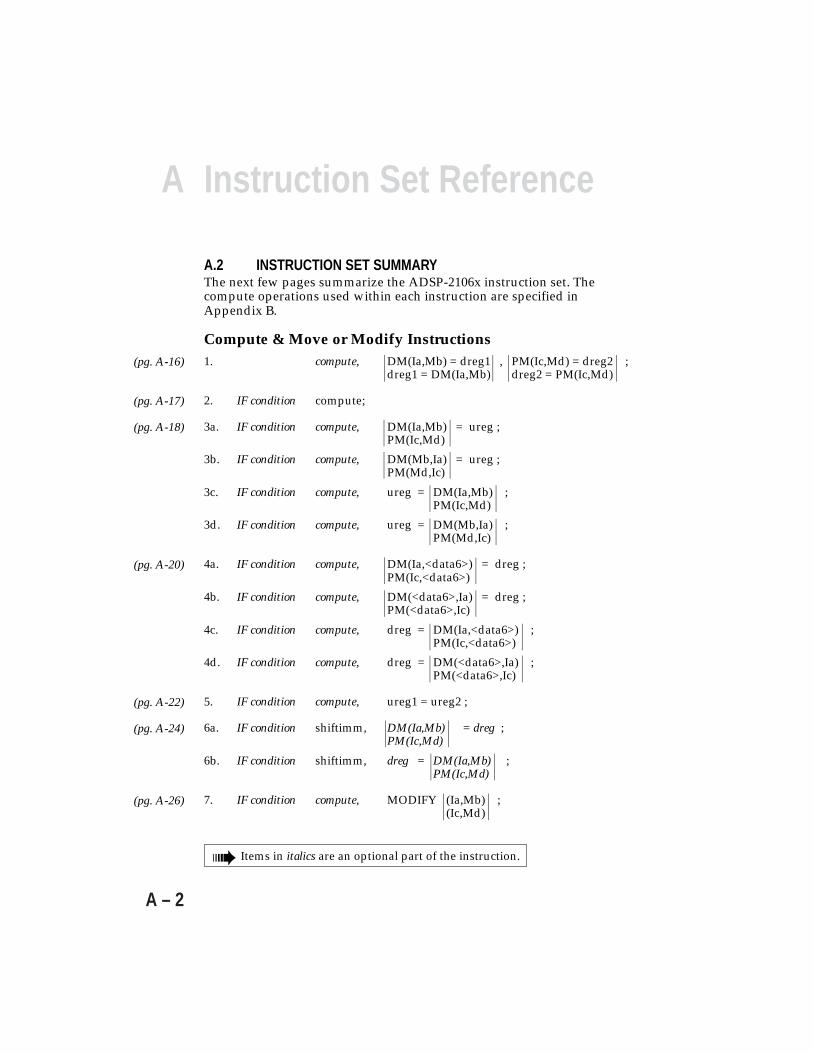
A.2 INSTRUCTION SET SUMMARYThe next few pages summarize the ADSP-2106x instruction set. Thecompute operations used within each instruction are specified inAppendix B.
(pg. A-16)
(pg. A-17)
(pg. A-18)
(pg. A-20)
(pg. A-22)
(pg. A-24)
(pg. A-26)
Compute & Move or Modify Instructions1. compute, DM(Ia,Mb) = dreg1 , PM(Ic,Md) = dreg2 ;
dreg1 = DM(Ia,Mb) dreg2 = PM(Ic,Md)
2. IF condition compute;
3a. IF condition compute, DM(Ia,Mb) = ureg ;PM(Ic,Md)
3b. IF condition compute, DM(Mb,Ia) = ureg ;PM(Md,Ic)
3c. IF condition compute, ureg = DM(Ia,Mb) ;PM(Ic,Md)
3d. IF condition compute, ureg = DM(Mb,Ia) ;PM(Md,Ic)
4a. IF condition compute, DM(Ia,<data6>) = dreg ;PM(Ic,<data6>)
4b. IF condition compute, DM(<data6>,Ia) = dreg ;PM(<data6>,Ic)
4c. IF condition compute, dreg = DM(Ia,<data6>) ;PM(Ic,<data6>)
4d. IF condition compute, dreg = DM(<data6>,Ia) ;PM(<data6>,Ic)
5. IF condition compute, ureg1 = ureg2 ;
6a. IF condition shiftimm, DM(Ia,Mb) = dreg ;PM(Ic,Md)
6b. IF condition shiftimm, dreg = DM(Ia,Mb) ;PM(Ic,Md)
7. IF condition compute, MODIFY (Ia,Mb) ;(Ic,Md)
➠ Items in italics are an optional part of the instruction.
AInstruction Set Reference
A – 3
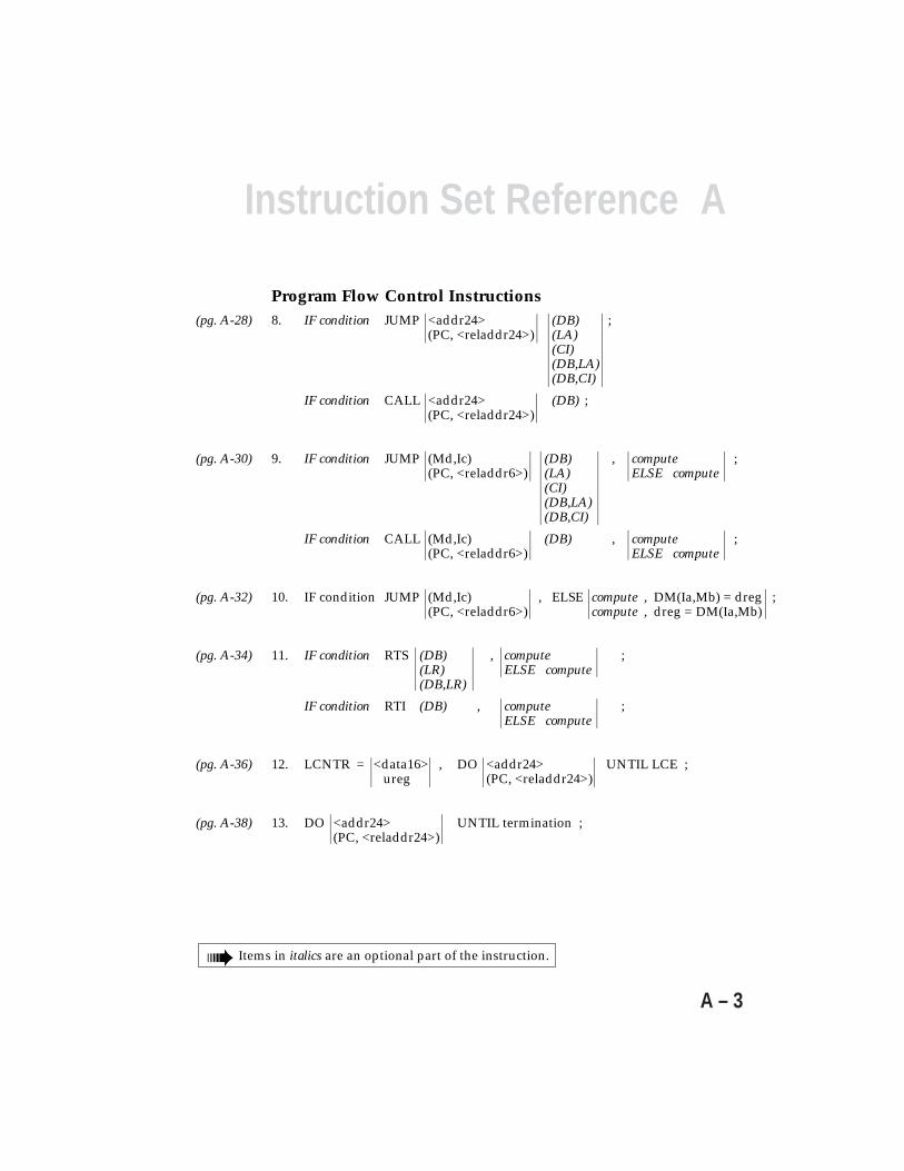
Program Flow Control Instructions8. IF condition JUMP <addr24> (DB) ;
(PC, <reladdr24>) (LA)(CI)(DB,LA)(DB,CI)
IF condition CALL <addr24> (DB) ;(PC, <reladdr24>)
9. IF condition JUMP (Md,Ic) (DB) , compute ;(PC, <reladdr6>) (LA) ELSE compute
(CI)(DB,LA)(DB,CI)
IF condition CALL (Md,Ic) (DB) , compute ;(PC, <reladdr6>) ELSE compute
10. IF condition JUMP (Md,Ic) , ELSE compute , DM(Ia,Mb) = dreg ;(PC, <reladdr6>) compute , dreg = DM(Ia,Mb)
11. IF condition RTS (DB) , compute ;(LR) ELSE compute(DB,LR)
IF condition RTI (DB) , compute ;ELSE compute
12. LCNTR = <data16> , DO <addr24> UNTIL LCE ; ureg (PC, <reladdr24>)
13. DO <addr24> UNTIL termination ;(PC, <reladdr24>)
(pg. A-28)
(pg. A-30)
(pg. A-32)
(pg. A-34)
(pg. A-36)
(pg. A-38)
➠ Items in italics are an optional part of the instruction.

Instruction Set ReferenceA
A – 4
(pg. A-46)
(pg. A-48)
(pg. A-50)
(pg. A-51)
(pg. A-52)
(pg. A-53)
(pg. A-54)
Immediate Move Instructions14a. DM(<addr32>) = ureg ;
PM(<addr24>)
14b. ureg = DM(<addr32>) ;PM(<addr24>)
15a. DM(<data32>, Ia) = ureg ;PM(<data24>, Ic)
15b. ureg = DM(<data32>, Ia) ;PM(<data24>, Ic)
16. DM(Ia,Mb) = <data32> ;PM(Ic,Md)
17. ureg = <data32> ;
(pg. A-40)
(pg. A-41)
(pg. A-42)
(pg. A-43)
Miscellaneous Instructions18. BIT SET sreg <data32> ;
CLRTGLTSTXOR
19a. MODIFY (Ia, <data32>) ;(Ic, <data24>)
19b. BITREV (Ia, <data32>) ;(Ic, <data24>)
20. PUSH LOOP , PUSH STS , PUSH PCSTK , FLUSH CACHE ;POP POP POP
21. NOP;
22. IDLE ;
23. IDLE16 ;
24. CJUMP function (DB) ;(PC, <reladdr24>)
RFRAME ;
Items in italics are an optional part of the instruction.➠
AInstruction Set Reference
A – 5
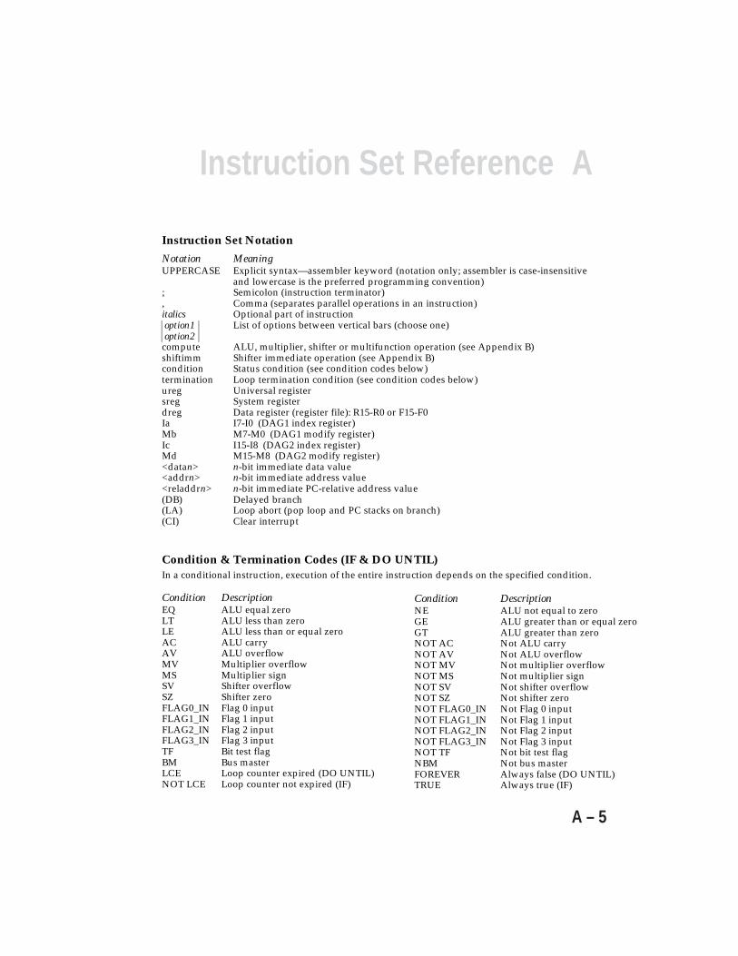
Instruction Set Notation
Notation MeaningUPPERCASE Explicit syntax—assembler keyword (notation only; assembler is case-insensitive
and lowercase is the preferred programming convention); Semicolon (instruction terminator), Comma (separates parallel operations in an instruction)italics Optional part of instruction option1 List of options between vertical bars (choose one) option2compute ALU, multiplier, shifter or multifunction operation (see Appendix B)shiftimm Shifter immediate operation (see Appendix B)condition Status condition (see condition codes below)termination Loop termination condition (see condition codes below)ureg Universal registersreg System registerdreg Data register (register file): R15-R0 or F15-F0Ia I7-I0 (DAG1 index register)Mb M7-M0 (DAG1 modify register)Ic I15-I8 (DAG2 index register)Md M15-M8 (DAG2 modify register)<datan> n-bit immediate data value<addrn> n-bit immediate address value<reladdrn> n-bit immediate PC-relative address value(DB) Delayed branch(LA) Loop abort (pop loop and PC stacks on branch)(CI) Clear interrupt
Condition & Termination Codes (IF & DO UNTIL)In a conditional instruction, execution of the entire instruction depends on the specified condition.
Condition DescriptionEQ ALU equal zeroLT ALU less than zeroLE ALU less than or equal zeroAC ALU carryAV ALU overflowMV Multiplier overflowMS Multiplier signSV Shifter overflowSZ Shifter zeroFLAG0_IN Flag 0 inputFLAG1_IN Flag 1 inputFLAG2_IN Flag 2 inputFLAG3_IN Flag 3 inputTF Bit test flagBM Bus masterLCE Loop counter expired (DO UNTIL)NOT LCE Loop counter not expired (IF)
Condition DescriptionNE ALU not equal to zeroGE ALU greater than or equal zeroGT ALU greater than zeroNOT AC Not ALU carryNOT AV Not ALU overflowNOT MV Not multiplier overflowNOT MS Not multiplier signNOT SV Not shifter overflowNOT SZ Not shifter zeroNOT FLAG0_IN Not Flag 0 inputNOT FLAG1_IN Not Flag 1 inputNOT FLAG2_IN Not Flag 2 inputNOT FLAG3_IN Not Flag 3 inputNOT TF Not bit test flagNBM Not bus masterFOREVER Always false (DO UNTIL)TRUE Always true (IF)
Instruction Set ReferenceA
A – 6
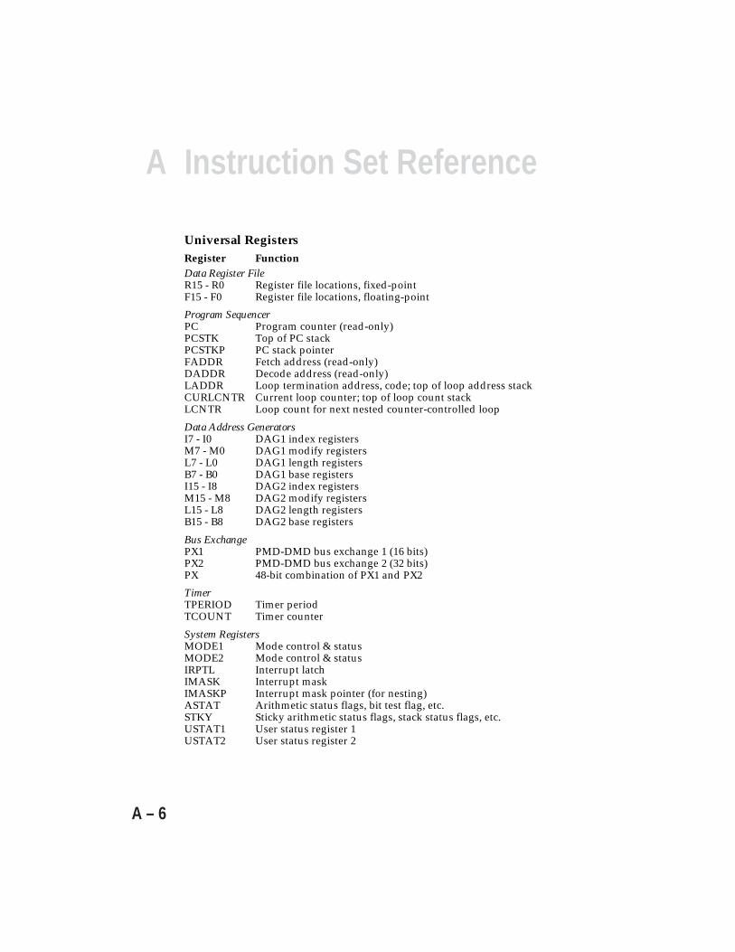
Universal RegistersRegister FunctionData Register FileR15 - R0 Register file locations, fixed-pointF15 - F0 Register file locations, floating-point
Program SequencerPC Program counter (read-only)PCSTK Top of PC stackPCSTKP PC stack pointerFADDR Fetch address (read-only)DADDR Decode address (read-only)LADDR Loop termination address, code; top of loop address stackCURLCNTR Current loop counter; top of loop count stackLCNTR Loop count for next nested counter-controlled loop
Data Address GeneratorsI7 - I0 DAG1 index registersM7 - M0 DAG1 modify registersL7 - L0 DAG1 length registersB7 - B0 DAG1 base registersI15 - I8 DAG2 index registersM15 - M8 DAG2 modify registersL15 - L8 DAG2 length registersB15 - B8 DAG2 base registers
Bus ExchangePX1 PMD-DMD bus exchange 1 (16 bits)PX2 PMD-DMD bus exchange 2 (32 bits)PX 48-bit combination of PX1 and PX2
TimerTPERIOD Timer periodTCOUNT Timer counter
System RegistersMODE1 Mode control & statusMODE2 Mode control & statusIRPTL Interrupt latchIMASK Interrupt maskIMASKP Interrupt mask pointer (for nesting)ASTAT Arithmetic status flags, bit test flag, etc.STKY Sticky arithmetic status flags, stack status flags, etc.USTAT1 User status register 1USTAT2 User status register 2

AInstruction Set Reference
A – 7
Memory Addressing in Instructions
Direct:
AbsoluteInstruction Types 8, 12, 13, 14Examples: dm(0x000015F0) = astat;
if ne jump label2; {'label2' is an address label}
PC-relativeInstruction Types 8, 9, 10, 12, 13Examples: call(pc,10), r0=r6+r3;
do(pc,length) until sz; {'length' is a variable}
Register Indirect (using DAG registers):
Post-modify with M register, update I registerInstruction Types 1, 3, 6, 16Examples: f5=pm(i9,m12);
dm(i0,m3)=r3, r1=pm(i15,m10);
Pre-modify with M register, no updateInstruction Types 3, 9, 10Examples: r1=pm(m10,i15);
jump(m13,i11);
Post-modify with immediate value, update I registerInstruction Type 4Examples: f15=dm(i0,6);
if av r1=pm(i15,0x11);
Pre-modify with immediate value, no updateInstruction Types 4, 15Examples: if av r1=pm(0x11,i15);
dm(127,i5)=laddr;

BCompute OperationReference
B.1 OVERVIEWCompute operations execute in the multiplier, the ALU and the shifter.The 23-bit compute field is like a mini-instruction within the ADSP-21000instruction and can be specified for a variety of compute operations. Thisappendix describes each compute operation in detail, including itsassembly language syntax and opcode field.
A compute operation is one of the following:
• Single-function operations involve a single computation unit.
• Multifunction operations specify parallel operation of the multiplier andthe ALU or two operations in the ALU.
• The MR register transfer is a special type of compute operation used toaccess the fixed-point accumulator in the multiplier. (See p. B-52).
The operations in each category are described in the following sections.For each operation, the assembly language syntax, the function, and theopcode format and contents are specified. Refer to the beginning ofAppendix A for an explanation of the notation and abbreviations used.
B.2 SINGLE-FUNCTION OPERATIONSThe compute field of a single-function operation looks like:
22 21 20 19 18 17 16 15 14 13 12 11 10 9 8 7 6 5 4 3 2 1 0
0 CU OPCODE RN RX RY
An operation determined by OPCODE is executed in the computation unitspecified by CU. The x- and the y-operands are received from dataregisters RX and RY. The result operand is returned to data register RN.
B – 1

B Compute Operations
B – 2
The CU (computation unit) field is defined as follows:
CU=00 ALU operationsCU=01 Multiplier operationsCU=10 Shifter operations
In some shifter operations, data register RN is used both as a destinationfor a result operand and as source for a third input operand.
The available operations and their 8-bit OPCODE values are listed in thefollowing sections, organized by computation unit: ALU, multiplier andshifter. In each section, the syntax and opcodes for the operations are firstsummarized and then the operations are described in detail.
B.2.1 ALU OperationsThe ALU operations are described in this section. Tables B.1 and B.2summarize the syntax and opcodes for the fixed-point and floating-pointALU operations, respectively. The rest of this section contains detaileddescriptions of each operation.
Syntax OpcodeRn = Rx + Ry 0000 0001Rn = Rx – Ry 0000 0010Rn = Rx + Ry + CI 0000 0101Rn = Rx – Ry + CI – 1 0000 0110Rn = (Rx + Ry)/2 0000 1001COMP(Rx, Ry) 0000 1010Rn = Rx + CI 0010 0101Rn = Rx + CI – 1 0010 0110Rn = Rx + 1 0010 1001Rn = Rx – 1 0010 1010Rn = –Rx 0010 0010Rn = ABS Rx 0011 0000Rn = PASS Rx 0010 0001Rn = Rx AND Ry 0100 0000Rn = Rx OR Ry 0100 0001Rn = Rx XOR Ry 0100 0010Rn = NOT Rx 0100 0011Rn = MIN(Rx, Ry) 0110 0001Rn = MAX(Rx, Ry) 0110 0010Rn = CLIP Rx BY Ry 0110 0011
Table B.1 Fixed-Point ALU Operations
BCompute Operations
B – 3
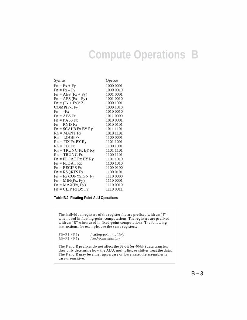
Syntax OpcodeFn = Fx + Fy 1000 0001Fn = Fx – Fy 1000 0010Fn = ABS (Fx + Fy) 1001 0001Fn = ABS (Fx – Fy) 1001 0010Fn = (Fx + Fy)/2 1000 1001COMP(Fx, Fy) 1000 1010Fn = –Fx 1010 0010Fn = ABS Fx 1011 0000Fn = PASS Fx 1010 0001Fn = RND Fx 1010 0101Fn = SCALB Fx BY Ry 1011 1101Rn = MANT Fx 1010 1101Rn = LOGB Fx 1100 0001Rn = FIX Fx BY Ry 1101 1001Rn = FIX Fx 1100 1001Rn = TRUNC Fx BY Ry 1101 1101Rn = TRUNC Fx 1100 1101Fn = FLOAT Rx BY Ry 1101 1010Fn = FLOAT Rx 1100 1010Fn = RECIPS Fx 1100 0100Fn = RSQRTS Fx 1100 0101Fn = Fx COPYSIGN Fy 1110 0000Fn = MIN(Fx, Fy) 1110 0001Fn = MAX(Fx, Fy) 1110 0010Fn = CLIP Fx BY Fy 1110 0011
Table B.2 Floating-Point ALU Operations
The individual registers of the register file are prefixed with an “F”when used in floating-point computations. The registers are prefixedwith an “R” when used in fixed-point computations. The followinginstructions, for example, use the same registers:
F0=F1 * F2; floating-point multiplyR0=R1 * R2; fixed-point multiply
The F and R prefixes do not affect the 32-bit (or 40-bit) data transfer;they only determine how the ALU, multiplier, or shifter treat the data.The F and R may be either uppercase or lowercase; the assembler iscase-insensitive.

BCompute Operations
B – 45
B.2.2 Multiplier OperationsThe multiplier operations are described in this section. Table B.3summarizes the syntax and opcodes for the fixed-point and floating-pointmultiplier operations. The rest of this section contains detaileddescriptions of each operation.
Fixed-point:Syntax OpcodeRn = Rx * Ry mod2† 01yx f00rMRF = Rx * Ry mod2† 01yx f10rMRB = Rx * Ry mod2† 01yx f11r
Rn = MRF + Rx * Ry mod2† 10yx f00rRn = MRB + Rx * Ry mod2† 10yx f01rMRF = MRF + Rx * Ry mod2† 10yx f10rMRB = MRB + Rx * Ry mod2† 10yx f11r
Rn = MRF – Rx * Ry mod2† 11yx f00rRn = MRB – Rx * Ry mod2† 11yx f01rMRF = MRF – Rx * Ry mod2† 11yx f10rMRB = MRB – Rx * Ry mod2† 11yx f11r
Rn = SAT MRF mod1†† 0000 f00xRn = SAT MRB mod1†† 0000 f01xMRF = SAT MRF mod1†† 0000 f10xMRB = SAT MRB mod1†† 0000 f11x
Rn = RND MRF mod1†† 0001 100xRn = RND MRB mod1†† 0001 101xMRF = RND MRF mod1†† 0001 110xMRB = RND MRB mod1†† 0001 111x
MRF = 0 0001 0100MRB = 0 0001 0110
MR = RnRn = MR
Floating-point:Syntax OpcodeFn = Fx * Fy 0011 0000
† See Table B.4†† See Table B.5
y y-input; 1=signed, 0=unsignedx x-input; 1=signed, 0=unsignedf format; 1=fractional, 0=integerr rounding; 1=yes, 0=no
Table B.3 Multiplier Operations

B Compute Operations
B – 46
Mod2 in Table B.3 is an optional modifier, enclosed in parentheses,consisting of three or four letters that indicate whether the x-input issigned (S) or unsigned (U), whether the y-input is signed or unsigned,whether the inputs are in integer (I) or fractional (F) format and whetherthe result when written to the register file is to be rounded-to-nearest (R).The options for mod2 and the corresponding opcode values are listed inTable B.4.
Mod2 Opcode(SSI) --11 0--0(SUI) --01 0--0(USI) --10 0--0(UUI) --00 0--0(SSF) --11 1--0(SUF) --01 1--0(USF) --10 1--0(UUF) --00 1--0(SSFR) --11 1--1(SUFR) --01 1--1(USFR) --10 1--1(UUFR) --00 1--1
Table B.4 Multiplier Mod2 Options
Similarly, mod1 in Table B.3 is an optional modifier, enclosed inparentheses, consisting of two letters that indicate whether the input issigned (S) or unsigned (U) and whether the input is in integer (I) orfractional (F) format. The options for mod1 and the corresponding opcodevalues are listed in Table B.5.
Mod1 Opcode(SI) (for SAT only) ---- 0--1(UI) (for SAT only) ---- 0--0(SF) ---- 1--1(UF) ---- 1--0
Table B.5 Multiplier Mod1 Options
B Compute Operations
B – 54
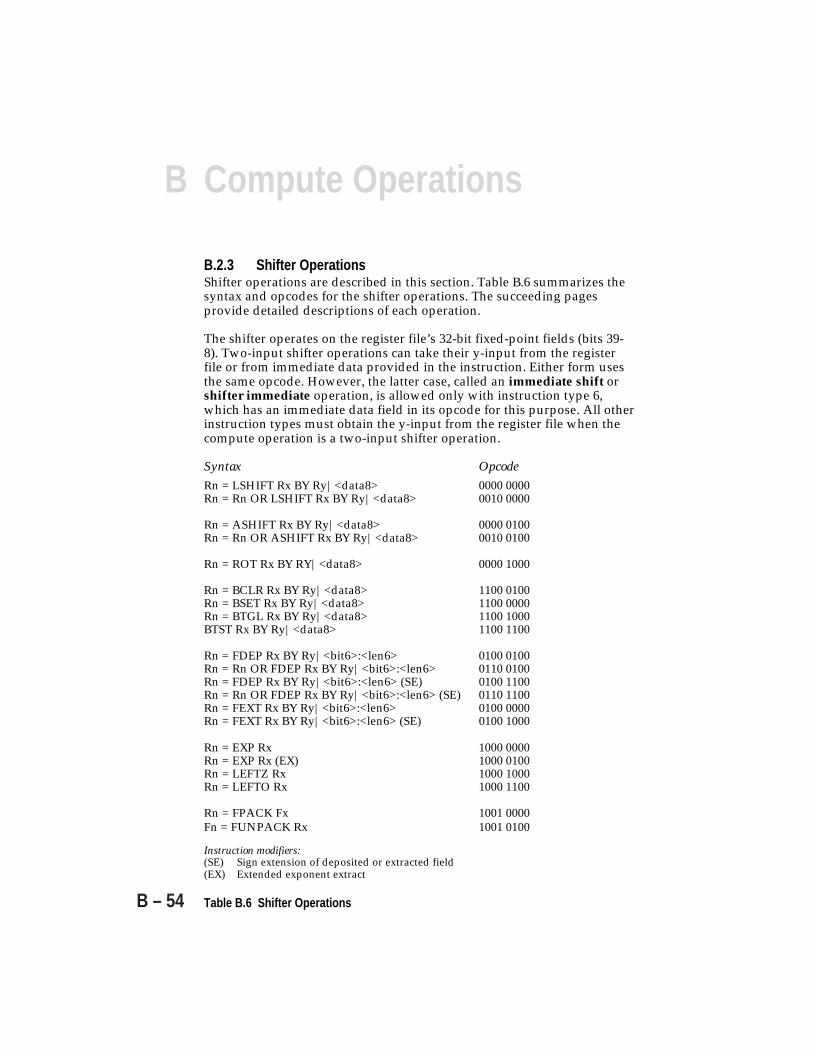
B.2.3 Shifter OperationsShifter operations are described in this section. Table B.6 summarizes thesyntax and opcodes for the shifter operations. The succeeding pagesprovide detailed descriptions of each operation.
The shifter operates on the register file’s 32-bit fixed-point fields (bits 39-8). Two-input shifter operations can take their y-input from the registerfile or from immediate data provided in the instruction. Either form usesthe same opcode. However, the latter case, called an immediate shift orshifter immediate operation, is allowed only with instruction type 6,which has an immediate data field in its opcode for this purpose. All otherinstruction types must obtain the y-input from the register file when thecompute operation is a two-input shifter operation.
Syntax OpcodeRn = LSHIFT Rx BY Ry|<data8> 0000 0000Rn = Rn OR LSHIFT Rx BY Ry|<data8> 0010 0000
Rn = ASHIFT Rx BY Ry|<data8> 0000 0100Rn = Rn OR ASHIFT Rx BY Ry|<data8> 0010 0100
Rn = ROT Rx BY RY|<data8> 0000 1000
Rn = BCLR Rx BY Ry|<data8> 1100 0100Rn = BSET Rx BY Ry|<data8> 1100 0000Rn = BTGL Rx BY Ry|<data8> 1100 1000BTST Rx BY Ry|<data8> 1100 1100
Rn = FDEP Rx BY Ry|<bit6>:<len6> 0100 0100Rn = Rn OR FDEP Rx BY Ry|<bit6>:<len6> 0110 0100Rn = FDEP Rx BY Ry|<bit6>:<len6> (SE) 0100 1100Rn = Rn OR FDEP Rx BY Ry|<bit6>:<len6> (SE) 0110 1100Rn = FEXT Rx BY Ry|<bit6>:<len6> 0100 0000Rn = FEXT Rx BY Ry|<bit6>:<len6> (SE) 0100 1000
Rn = EXP Rx 1000 0000Rn = EXP Rx (EX) 1000 0100Rn = LEFTZ Rx 1000 1000Rn = LEFTO Rx 1000 1100
Rn = FPACK Fx 1001 0000Fn = FUNPACK Rx 1001 0100
Instruction modifiers:(SE) Sign extension of deposited or extracted field(EX) Extended exponent extract
Table B.6 Shifter Operations
B Compute Operations
B – 76
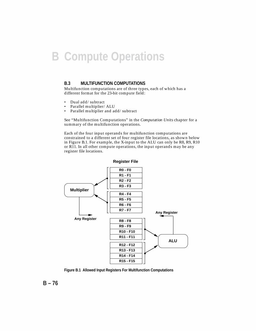
B.3 MULTIFUNCTION COMPUTATIONSMultifunction computations are of three types, each of which has adifferent format for the 23-bit compute field:
• Dual add/subtract• Parallel multiplier/ALU• Parallel multiplier and add/subtract
See “Multifunction Computations” in the Computation Units chapter for asummary of the multifunction operations.
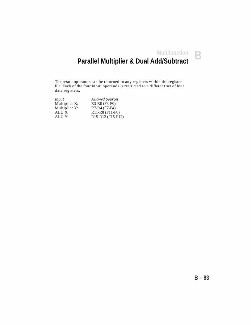
Each of the four input operands for multifunction computations areconstrained to a different set of four register file locations, as shown belowin Figure B.1. For example, the X-input to the ALU can only be R8, R9, R10or R11. In all other compute operations, the input operands may be anyregister file locations.
R0 - F0R1 - F1R2 - F2
R3 - F3
R4 - F4R5 - F5
R6 - F6R7 - F7
R8 - F8R9 - F9
R10 - F10R11 - F11
R12 - F12R13 - F13
R14 - F14R15 - F15
Multiplier
ALU
Any Register
Any Register
Register File
Figure B.1 Allowed Input Registers For Multifunction Computations
B Compute Operations
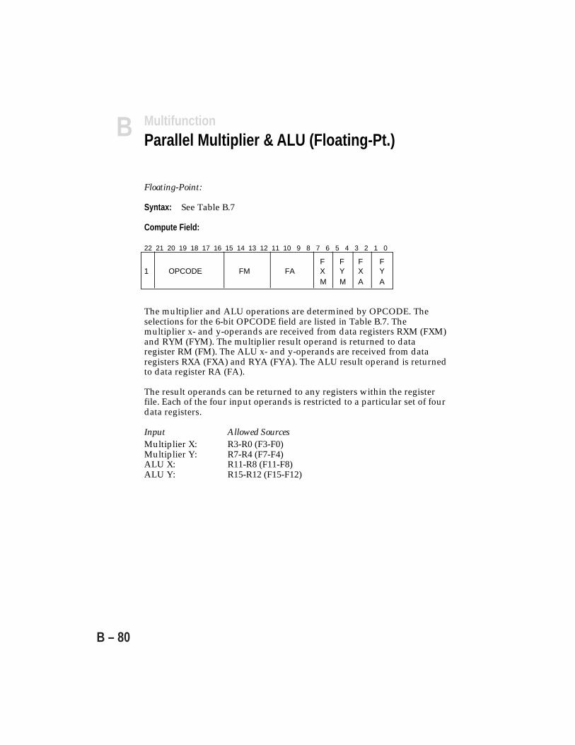
B – 80
Floating-Point:
Syntax: See Table B.7
Compute Field:
22 21 20 19 18 17 16 15 14 13 12 11 10 9 8 7 6 5 4 3 2 1 0
F F F F1 OPCODE FM FA X Y X Y
M M A A
The multiplier and ALU operations are determined by OPCODE. Theselections for the 6-bit OPCODE field are listed in Table B.7. Themultiplier x- and y-operands are received from data registers RXM (FXM)and RYM (FYM). The multiplier result operand is returned to dataregister RM (FM). The ALU x- and y-operands are received from dataregisters RXA (FXA) and RYA (FYA). The ALU result operand is returnedto data register RA (FA).
The result operands can be returned to any registers within the registerfile. Each of the four input operands is restricted to a particular set of fourdata registers.
Input Allowed SourcesMultiplier X: R3-R0 (F3-F0)Multiplier Y: R7-R4 (F7-F4)ALU X: R11-R8 (F11-F8)ALU Y: R15-R12 (F15-F12)
MultifunctionParallel Multiplier & ALU (Floating-Pt.)
BCompute Operations
B – 81
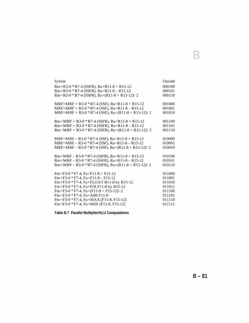
Syntax OpcodeRm=R3-0 * R7-4 (SSFR), Ra=R11-8 + R15-12 000100Rm=R3-0 * R7-4 (SSFR), Ra=R11-8 – R15-12 000101Rm=R3-0 * R7-4 (SSFR), Ra=(R11-8 + R15-12)/2 000110
MRF=MRF + R3-0 * R7-4 (SSF), Ra=R11-8 + R15-12 001000MRF=MRF + R3-0 * R7-4 (SSF), Ra=R11-8 – R15-12 001001MRF=MRF + R3-0 * R7-4 (SSF), Ra=(R11-8 + R15-12)/2 001010
Rm=MRF + R3-0 * R7-4 (SSFR), Ra=R11-8 + R15-12 001100Rm=MRF + R3-0 * R7-4 (SSFR), Ra=R11-8 – R15-12 001101Rm=MRF + R3-0 * R7-4 (SSFR), Ra=(R11-8 + R15-12)/2 001110
MRF=MRF – R3-0 * R7-4 (SSF), Ra=R11-8 + R15-12 010000MRF=MRF – R3-0 * R7-4 (SSF), Ra=R11-8 – R15-12 010001MRF=MRF – R3-0 * R7-4 (SSF), Ra=(R11-8 + R15-12)/2 010010
Rm=MRF – R3-0 * R7-4 (SSFR), Ra=R11-8 + R15-12 010100Rm=MRF – R3-0 * R7-4 (SSFR), Ra=R11-8 – R15-12 010101Rm=MRF – R3-0 * R7-4 (SSFR), Ra=(R11-8 + R15-12)/2 010110
Fm=F3-0 * F7-4, Fa=F11-8 + F15-12 011000Fm=F3-0 * F7-4, Fa=F11-8 – F15-12 011001Fm=F3-0 * F7-4, Fa=FLOAT R11-8 by R15-12 011010Fm=F3-0 * F7-4, Fa=FIX F11-8 by R15-12 011011Fm=F3-0 * F7-4, Fa=(F11-8 + F15-12)/2 011100Fm=F3-0 * F7-4, Fa=ABS F11-8 011101Fm=F3-0 * F7-4, Fa=MAX (F11-8, F15-12) 011110Fm=F3-0 * F7-4, Fa=MIN (F11-8, F15-12) 011111
Table B.7 Parallel Multiplier/ALU Computations

B Compute Operations
B – 82
The parallel multiplier and dual add/subtract operation performs amultiply or multiply/accumulate and computes the sum and thedifference of the ALU inputs. For detailed information on the multiplieroperations, see the individual descriptions under Single-FunctionOperations. For information on the dual add/subtract operation, see theDual Add/Subtract section.
Fixed-Point:
Syntax:
Rm=R3-0 * R7-4 (SSFR), Ra=R11-8 + R15-12, Rs=R11-8 – R15-12
Compute Field:
22 21 20 19 18 17 16 15 14 13 12 11 10 9 8 7 6 5 4 3 2 1 0
R R R R1 1 0 RS RM RA X Y X Y
M M A A
Floating-Point:
Syntax:
Fm=F3-0 * F7-4, Fa=F11-8 + F15-12, Fs=F11-8 – F15-12
Compute Field:
22 21 20 19 18 17 16 15 14 13 12 11 10 9 8 7 6 5 4 3 2 1 0
F F F F1 1 1 FS FM FA X Y X Y
M M A A
The multiplier x- and y-operands are received from data registers RXM(FXM) and RYM (FYM). The multiplier result operand is returned to dataregister RM (FM). The ALU x- and y-operands are received from dataregisters RXA (FXA) and RYA (FYA). The ALU result operands arereturned to data register RA (FA) and RS (FS).
MultifunctionParallel Multiplier & Dual Add/Subtract
BCompute Operations
B – 83
The result operands can be returned to any registers within the registerfile. Each of the four input operands is restricted to a different set of fourdata registers.
Input Allowed SourcesMultiplier X: R3-R0 (F3-F0)Multiplier Y: R7-R4 (F7-F4)ALU X: R11-R8 (F11-F8)ALU Y: R15-R12 (F15-F12)
MultifunctionParallel Multiplier & Dual Add/Subtract
F
F – 1
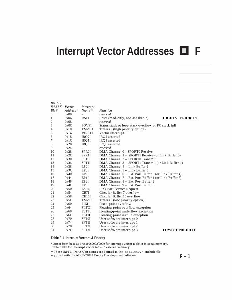
Interrupt Vector Addresses
IRPTL/IMASK Vector InterruptBit # Address* Name** Function0 0x00 – reserved1 0x04 RSTI Reset (read-only, non-maskable) HIGHEST PRIORITY2 0x08 – reserved3 0x0C SOVFI Status stack or loop stack overflow or PC stack full4 0x10 TMZHI Timer=0 (high priority option)5 0x14 VIRPTI Vector Interrupt6 0x18 IRQ2I IRQ2 asserted7 0x1C IRQ1I IRQ1 asserted8 0x20 IRQ0I IRQ0 asserted9 0x24 – reserved10 0x28 SPR0I DMA Channel 0 – SPORT0 Receive11 0x2C SPR1I DMA Channel 1 – SPORT1 Receive (or Link Buffer 0)12 0x30 SPT0I DMA Channel 2 – SPORT0 Transmit13 0x34 SPT1I DMA Channel 3 – SPORT1 Transmit (or Link Buffer 1)14 0x38 LP2I DMA Channel 4 – Link Buffer 215 0x3C LP3I DMA Channel 5 – Link Buffer 316 0x40 EP0I DMA Channel 6 – Ext. Port Buffer 0 (or Link Buffer 4)17 0x44 EP1I DMA Channel 7 – Ext. Port Buffer 1 (or Link Buffer 5)18 0x48 EP2I DMA Channel 8 – Ext. Port Buffer 219 0x4C EP3I DMA Channel 9 – Ext. Port Buffer 320 0x50 LSRQ Link Port Service Request21 0x54 CB7I Circular Buffer 7 overflow22 0x58 CB15I Circular Buffer 15 overflow23 0x5C TMZLI Timer=0 (low priority option)24 0x60 FIXI Fixed-point overflow25 0x64 FLTOI Floating-point overflow exception26 0x68 FLTUI Floating-point underflow exception27 0x6C FLTII Floating-point invalid exception28 0x70 SFT0I User software interrupt 029 0x74 SFT1I User software interrupt 130 0x78 SFT2I User software interrupt 231 0x7C SFT3I User software interrupt 3 LOWEST PRIORITY
Table F.1 Interrupt Vectors & Priority
* Offset from base address: 0x0002 0000 for interrupt vector table in internal memory,0x0040 0000 for interrupt vector table in external memory** These IRPTL/IMASK bit names are defined in the def21060.h include filesupplied with the ADSP-21000 Family Development Software.