1. general description - mouser electronics. general description ... xxxx...
TRANSCRIPT
1. General description
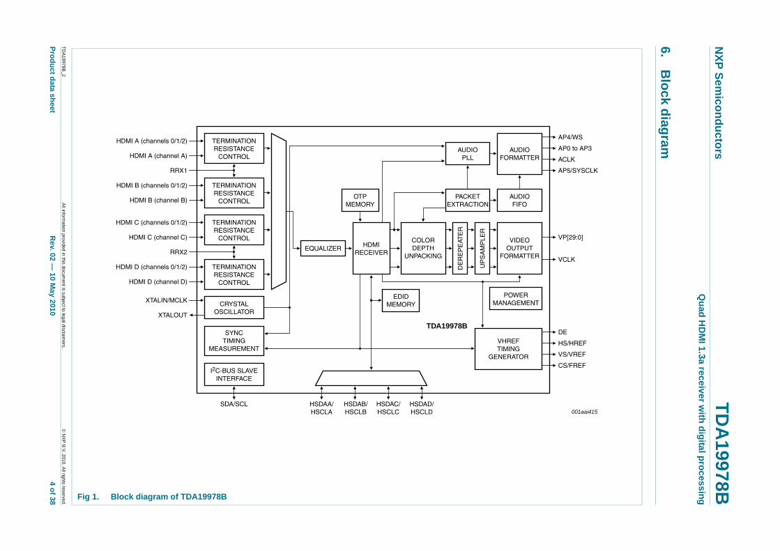
The TDA19978B is a four input HDMI 1.3a compliant receiver with embedded EDID memory. The built-in auto-adaptive equalizer improves signal quality and allows the use of cable lengths up to 25 m which are laboratory tested with a 0.5 mm (24 AWG) cable at 2.05 gigasamples per second. In addition, the TDA19978B is delivered with software drivers to ease configuration and use.
The TDA19978B supports:
• TV resolutions:– 480i (1440 × 480i at 60 Hz), 576i (1440 × 576i at 50 Hz) to HDTV (up to
1920 × 1080p at 50/60 Hz)– WUXGA (1920 × 1200p at 60 Hz) reduced blanking format
• PC resolutions:– VGA (640 × 480p at 60 Hz) to UXGA (1600 × 1200p at 60 Hz)
• Deep Color mode in 10-bit and 12-bit (up to 205 MHz TMDS clock)• Gamut boundary description• IEC 60958/IEC 61937, OBA (One Bit Audio), DST (Direct Stream Transfer) and HBR
(High Bit Rate) stream
The TDA19978B includes:
• An enhanced PC and TV format recognition system• Generation of a 128/256/512 × fs system clock allowing the use of simple audio DACs
without an integrated PLL (such as the UDA1334BTS)• An embedded oscillator (an external crystal can also be used)• Improved audio clock generation using an external reference clock• OBA (as used in SACD), DST and HBR stream support
The TDA19978B converts HDMI streams without HDCP into RGB or YCbCr digital signals. The YCbCr digital output signal can be 4:4:4 or 4:2:2 semi-planar format based on the ITU-R BT.601 standard or 4:2:2 based on the ITU-R BT.656 format. The device can adjust the output timing of the video port by altering the values of tsu(Q) and th(Q). In addition, all settings are controllable using the I2C-bus.
TDA19978BQuad HDMI 1.3a receiver interface with equalizer (HDTV up to 1080p, up to UXGA for PC formats)Rev. 02 — 10 May 2010 Product data sheet
NXP Semiconductors TDA19978BQuad HDMI 1.3a receiver with digital processing
2. Features and benefits
Complies with the HDMI 1.3a, DVI 1.0 and CEA-861-DFour (quad) independent HDMI inputs, up to the HDMI frequency of 205 MHzEmbedded auto-adaptive equalizer on all HDMI linksEDID memory: 253 shared bytes and three bytes dedicated to each HDMI inputSupports color depth processing (8-bit, 10-bit or 12-bit per color)Color gamut metadata packet with interrupt on each update, readable via the I2C-busUp to four S/PDIF or I2S-bus outputs (eight channels) at a sampling rate up to 192 kHz with IEC 60958/IEC 61937 streamHBR audio stream up to 768 kHz with four demultiplexed S/PDIF or I2S-bus outputsHBR streams (e.g. DTS-HD master audio and Dolby TrueHD up to eight channels due to HBR packet for stream with a frame rate up to 768 kHz) supportDSD and DST audio stream up to six DSD channels output for SACD with DST audio packet supportChannel status decoder supports multi-channel receptionImproved audio clock generation using an external reference clockSystem/master clock output (128/256/512 × fs) enables the use of the UDA1334BTSThe HDMI interface supports:
All HDTV formats up to 1920 × 1080p at 50/60 Hz and WUXGA (1920 × 1200p at 60 Hz) with support for reduced blankingPC formats up to UXGA (1600 × 1200p at 60 Hz)
Embedded oscillator (an external crystal can be used)Frame and field detection for interlaced video signalSync timing measurements for format recognitionImproved system for measurements of blanking and video active area allowing an accurate recognition of PC and TV formatsRepeater capabilityProgrammable color space input signal conversion from RGB-to-YCbCr or YCbCr-to-RGBOutput formats: RGB 4:4:4, YCbCr 4:4:4, YCbCr 4:2:2 semi-planar based on the ITU-R BT.601 standard and YCbCr 4:2:2 ITU-R BT.6568-bit, 10-bit or 12-bit output formats selectable using the I2C-bus (8-bit and 10-bit only in 4:4:4 format)I2C-bus adjustable timing of video port (tsu(Q) and th(Q))Downsampling-by-two with selectable filters on Cb and Cr channels in 4:2:2 modeInternal video and audio pattern generatorControllable using the I2C-bus; 5 V tolerant and bit rate up to 400 kbit/sDDC-bus inputs 5 V tolerant and bit rate up to 400 kbit/sLV-TTL outputsPower-down modeCMOS process1.8 V and 3.3 V power suppliesLead-free (Pb) HLQFP144 package
TDA19978B_2 All information provided in this document is subject to legal disclaimers. © NXP B.V. 2010. All rights reserved.
Product data sheet Rev. 02 — 10 May 2010 2 of 38
NXP Semiconductors TDA19978BQuad HDMI 1.3a receiver with digital processing
3. Applications
4. Quick reference data
[1] x = A, B, C or D.
[2] At 30 % activity on video port output.
5. Ordering information
HDTV High-end TVYCbCr or RGB high-speed video digitizer Home theater amplifierProjector, plasma and LCD TV DVD recorderRear projection TV AVR and HDMI splitter
Table 1. Quick reference dataSymbol Parameter Conditions Min Typ Max UnitDigital inputs: pins RXxC+, RXxC−[1]
fclk(max) maximum clock frequency 205 - - MHz
Clock timing output: pins VCLK, ACLK and SYSCLKfclk(max) maximum clock frequency pin VCLK 165 - - MHz
pin ACLK 25 - - MHz
pin SYSCLK 50 - - MHz
SuppliesVDDH(3V3) HDMI supply voltage (3.3 V) 3.135 3.3 3.465 V
VDDH(1V8) HDMI supply voltage (1.8 V) 1.71 1.8 1.89 V
VDDI(3V3) input supply voltage (3.3 V) 3.135 3.3 3.465 V
VDDC(1V8) core supply voltage (1.8 V) 1.71 1.8 1.89 V
VDDO(3V3) output supply voltage (3.3 V) 3.135 3.3 3.465 V
P power dissipation Active mode [2]
720p at 60 Hz - 0.75 - W
1080p at 60 Hz - 1.13 - W
1080p at 60 Hz; Deep Color mode - 1.63 - W
Pcons power consumption Power-down mode
pin PD = HIGH - 1 - mW
I2C-bus; EDID - 4 - mW
I2C-bus; EDID; activity detection - 150 - mW
Table 2. Ordering informationType number Package
Name Description VersionTDA19978BHV HLQFP144 plastic thermal enhanced low profile quad flat package;
144 leads; body 20 × 20 × 1.4 mm; exposed die padSOT612-3
TDA19978B_2 All information provided in this document is subject to legal disclaimers. © NXP B.V. 2010. All rights reserved.
Product data sheet Rev. 02 — 10 May 2010 3 of 38
xxxx xxxxxxxxxxxxxxxxxxxxxxxxxxxxxx x xxxxxxxxxxxxxx xxxxxxxxxx xxx xxxxxx xxxxxxxxxxxxxxxxxxxxxxx xxxxxxxxxxxxxxxxxxxxxx xxxxx xxxxxx xx xxxxxxxxxxxxxxxxxxxxxxxxxxxxx xxxxxxxxxxxxxxxxxxxxxx xxxxxxxxxxx xxxxxxx xxxxxxxxxxxxxxxxxxx xxxxxxxxxxxxxxxx xxxxxxxxxxxxxx xxxxxx xx xxxxxxxxxxxxxxxxxxxxxxxxxxxxxxxx xxxxxxxxxxxxxxxxxxxxxxxx xxxxxxx xxxxxxxxxxxxxxxxxxxxxxxxxxxxxxxxxxxxxxxxxxxxxx xxxxxxxxxxx xxxxx x x
TDA19978B
_2
Product data sh
NXP Sem
iconducto
6. B
lock diagra
AP4/WS
eet
rsTD
A19978B
Quad H
DM
I 1.3a receiver with digital processing
m
001aai415
AP0 to AP3
ACLK
AP5/SYSCLK
DE
HS/HREF
VS/VREF
CS/FREF
IDEOTPUTATTER
EREMENT
FGTOR
DIOIFO
DIOATTER
VP[29:0]
VCLK
All information provided in this docum
ent is subject to legal disclaimers.
© N
XP B.V. 2010. All rights reserved.
Rev. 02 —
10 May 2010
4 of 38 Fig 1. Block diagram of TDA19978B
HDMI A (channels 0/1/2)
HDMI A (channel A)
XTALIN/MCLK
XTALOUT
RRX1
SDA/SCL HSDAA/HSCLA
HSDAB/HSCLB
HSDAC/HSCLC
TDA19978BSYNC
TIMINGMEASUREMENT
I2C-BUS SLAVEINTERFACE
CRYSTALOSCILLATOR
TERMINATIONRESISTANCE
CONTROL
HDMI B (channels 0/1/2)
HDMI B (channel B)
TERMINATIONRESISTANCE
CONTROL
EDIDMEMORY
OTPMEMORY
HDMIRECEIVER
COLORDEPTH
UNPACKING
VOU
FORM
POWMANAG
VHRETIMIN
GENERA
AUF
PACKETEXTRACTION
AUDIOPLL
AUFORM
EQUALIZER
DE
RE
PE
ATE
R
UP
SA
MP
LER
HSDAD/HSCLD
HDMI C (channels 0/1/2)
HDMI C (channel C)
RRX2
TERMINATIONRESISTANCE
CONTROL
HDMI D (channels 0/1/2)
HDMI D (channel D)
TERMINATIONRESISTANCE
CONTROL
NXP Semiconductors TDA19978BQuad HDMI 1.3a receiver with digital processing
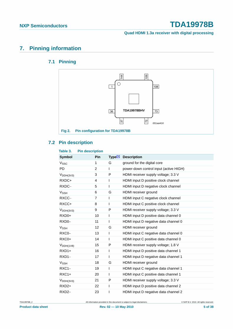
7. Pinning information
7.1 Pinning
7.2 Pin description
Fig 2. Pin configuration for TDA19978B
TDA19978BHV
001aai416
108
37 72
144
109
73
1
36
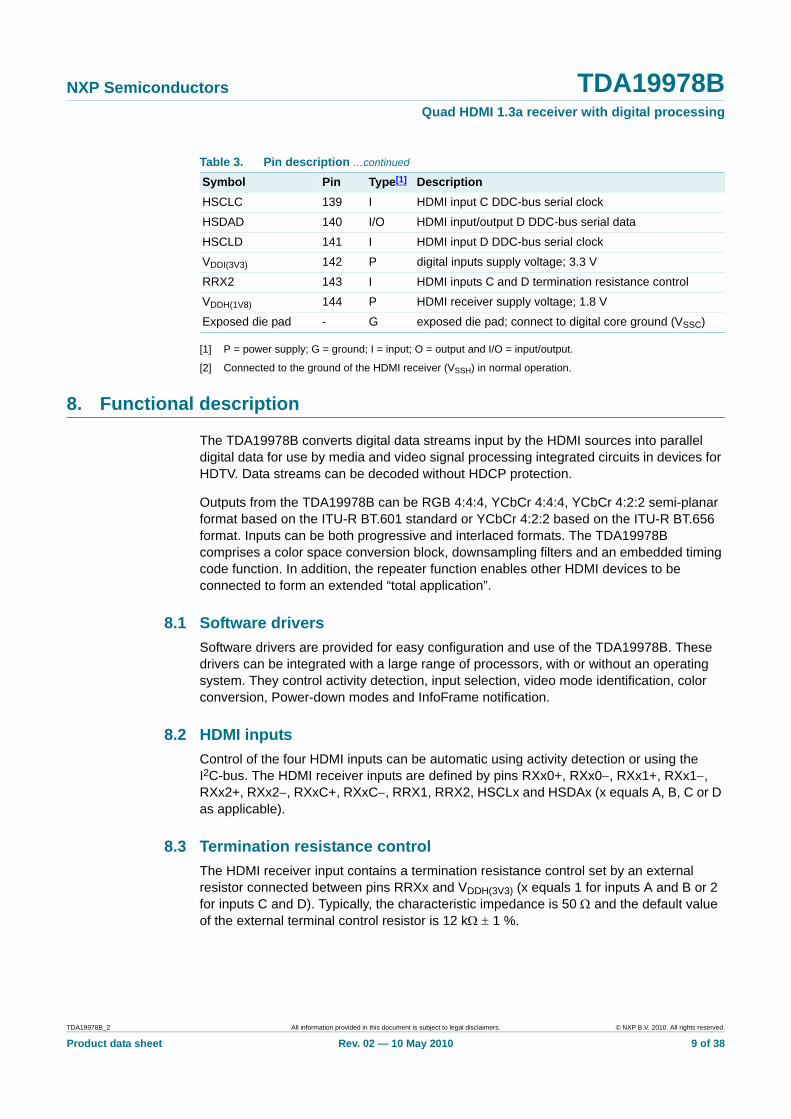
Table 3. Pin descriptionSymbol Pin Type[1] DescriptionVSSC 1 G ground for the digital core
PD 2 I power-down control input (active HIGH)
VDDH(3V3) 3 P HDMI receiver supply voltage; 3.3 V
RXDC+ 4 I HDMI input D positive clock channel
RXDC− 5 I HDMI input D negative clock channel
VSSH 6 G HDMI receiver ground
RXCC− 7 I HDMI input C negative clock channel
RXCC+ 8 I HDMI input C positive clock channel
VDDH(3V3) 9 P HDMI receiver supply voltage; 3.3 V
RXD0+ 10 I HDMI input D positive data channel 0
RXD0− 11 I HDMI input D negative data channel 0
VSSH 12 G HDMI receiver ground
RXC0− 13 I HDMI input C negative data channel 0
RXC0+ 14 I HDMI input C positive data channel 0
VDDH(1V8) 15 P HDMI receiver supply voltage; 1.8 V
RXD1+ 16 I HDMI input D positive data channel 1
RXD1− 17 I HDMI input D negative data channel 1
VSSH 18 G HDMI receiver ground
RXC1− 19 I HDMI input C negative data channel 1
RXC1+ 20 I HDMI input C positive data channel 1
VDDH(3V3) 21 P HDMI receiver supply voltage; 3.3 V
RXD2+ 22 I HDMI input D positive data channel 2
RXD2− 23 I HDMI input D negative data channel 2
TDA19978B_2 All information provided in this document is subject to legal disclaimers. © NXP B.V. 2010. All rights reserved.
Product data sheet Rev. 02 — 10 May 2010 5 of 38
NXP Semiconductors TDA19978BQuad HDMI 1.3a receiver with digital processing
VSSH 24 G HDMI receiver ground
RXC2− 25 I HDMI input C negative data channel 2
RXC2+ 26 I HDMI input C positive data channel 2
VPP 27 P OTP memory programming voltage[2]
VDDC(1V8) 28 P digital core supply voltage; 1.8 V
VDDO(3V3) 29 P video port output supply voltage; 3.3 V
VCLK 30 O video clock output
VSSO 31 G video port output ground
CS/FREF 32 O composite synchronization outputcomposite field output signal
VS/VREF 33 O vertical synchronization outputvertical reference output
HS/HREF 34 O horizontal synchronization outputhorizontal reference output
DE 35 O data enable output
VP[0] 36 O video port output bit 0
VSSC 37 G digital core ground
VP[1] 38 O video port output bit 1
VP[2] 39 O video port output bit 2
VP[3] 40 O video port output bit 3
VDDO(3V3) 41 P video port output supply voltage; 3.3 V
VDDC(1V8) 42 P digital core supply voltage; 1.8 V
VSSO 43 G video port output ground
VP[4] 44 O video port output bit 4
VP[5] 45 O video port output bit 5
VP[6] 46 O video port output bit 6
VP[7] 47 O video port output bit 7
VP[8] 48 O video port output bit 8
VP[9] 49 O video port output bit 9
VP[10] 50 O video port output bit 10
VP[11] 51 O video port output bit 11
VDDO(3V3) 52 P video port output supply voltage; 3.3 V
VP[12] 53 O video port output bit 12
VSSO 54 G video port output ground
VP[13] 55 O video port output bit 13
VP[14] 56 O video port output bit 14
VP[15] 57 O video port output bit 15
VP[16] 58 O video port output bit 16
VP[17] 59 O video port output bit 17
VP[18] 60 O video port output bit 18
VP[19] 61 O video port output bit 19
Table 3. Pin description …continued
Symbol Pin Type[1] Description
TDA19978B_2 All information provided in this document is subject to legal disclaimers. © NXP B.V. 2010. All rights reserved.
Product data sheet Rev. 02 — 10 May 2010 6 of 38
NXP Semiconductors TDA19978BQuad HDMI 1.3a receiver with digital processing
VP[20] 62 O video port output bit 20
VDDO(3V3) 63 P video port output supply voltage; 3.3 V
VDDC(1V8) 64 P digital core supply voltage; 1.8 V
VSSO 65 G video port output ground
VP[21] 66 O video port output bit 21
VP[22] 67 O video port output bit 22
VP[23] 68 O video port output bit 23
VP[24] 69 O video port output bit 24
VP[25] 70 O video port output bit 25
VP[26] 71 O video port output bit 26
VP[27] 72 O video port output bit 27
VSSC 73 G digital core ground
VDDO(3V3) 74 P video port output supply voltage; 3.3 V
VP[28] 75 O video port output bit 28
VP[29] 76 O video port output bit 29
VSSO 77 G video port output ground
ACLK 78 O audio clock output
AP0 79 O audio port 0 output
AP1 80 O audio port 1 output
AP2 81 O audio port 2 output
AP3 82 O audio port 3 output
AP4/WS 83 O audio port 4 outputword select output
VDDO(3V3) 84 P video port output supply voltage; 3.3 V
AP5/SYSCLK 85 O audio port 5 outputsystem clock audio output
VSSO 86 G video port output ground
VDDH(3V3) 87 P HDMI audio PLL supply voltage; 3.3 V
VDDH(3V3) 88 P HDMI audio PLL supply voltage; 3.3 V
VSSH 89 G HDMI audio PLL ground
VDDH(1V8) 90 P HDMI audio PLL supply voltage; 1.8 V
VSSH 91 G HDMI audio PLL ground
VDDC(1V8) 92 P digital core supply voltage; 1.8 V
XTALOUT 93 O crystal oscillator output
XTALIN/MCLK 94 I crystal oscillator inputtest pattern clock input
VDDI(3V3) 95 P digital inputs supply voltage; 3.3 V
VAI 96 O video activity indication output (open-drain); warns the external microprocessor that a special event has occurred; must be connected to a pull-up resistor; 5 V tolerant (active LOW)
SDA 97 I/O I2C-bus serial data input/output
Table 3. Pin description …continued
Symbol Pin Type[1] Description
TDA19978B_2 All information provided in this document is subject to legal disclaimers. © NXP B.V. 2010. All rights reserved.
Product data sheet Rev. 02 — 10 May 2010 7 of 38
NXP Semiconductors TDA19978BQuad HDMI 1.3a receiver with digital processing
SCL 98 I I2C-bus serial clock input
HSDAA 99 I/O HDMI input/output A DDC-bus serial data
HSCLA 100 I HDMI input A DDC-bus serial clock
HSDAB 101 I/O HDMI input/output B DDC-bus serial data
HSCLB 102 I HDMI input B DDC-bus serial clock
TEST0 103 I reserved for test; connect to digital inputs ground (VSSC)
VDDH(3V3) 104 P HDMI deep PLL supply voltage; 3.3 V
VSSH 105 G HDMI deep PLL ground
RRX1 106 I HDMI inputs A and B termination resistance control
VDDC(1V8) 107 P digital core supply voltage; 1.8 V
VDDH(1V8) 108 P HDMI receiver supply voltage; 1.8 V
VSSC 109 G digital core ground
A0 110 I I2C-bus address control input
VDDH(3V3) 111 P HDMI receiver supply voltage; 3.3 V
RXBC+ 112 I HDMI input B positive clock channel
RXBC− 113 I HDMI input B negative clock channel
VSSH 114 G HDMI receiver ground
RXAC− 115 I HDMI input A negative clock channel
RXAC+ 116 I HDMI input A positive clock channel
VDDH(3V3) 117 P HDMI receiver supply voltage; 3.3 V
RXB0+ 118 I HDMI input B positive data channel 0
RXB0− 119 I HDMI input B negative data channel 0
VSSH 120 G HDMI receiver ground
RXA0− 121 I HDMI input A negative data channel 0
RXA0+ 122 I HDMI input A positive data channel 0
VDDH(1V8) 123 P HDMI receiver supply voltage; 1.8 V
RXB1+ 124 I HDMI input B positive data channel 1
RXB1− 125 I HDMI input B negative data channel 1
VSSH 126 G HDMI receiver ground
RXA1− 127 I HDMI input A negative data channel 1
RXA1+ 128 I HDMI input A positive data channel 1
VDDH(3V3) 129 P HDMI receiver supply voltage; 3.3 V
RXB2+ 130 I HDMI input B positive data channel 2
RXB2− 131 I HDMI input B negative data channel 2
VSSH 132 G HDMI receiver ground
RXA2− 133 I HDMI input A negative data channel 2
RXA2+ 134 I HDMI input A positive data channel 2
VSSH 135 G HDMI receiver ground
VDDC(1V8) 136 P digital core supply voltage; 1.8 V
VDDC(1V8) 137 P digital core supply voltage; 1.8 V
HSDAC 138 I/O HDMI input/output C DDC-bus serial data
Table 3. Pin description …continued
Symbol Pin Type[1] Description
TDA19978B_2 All information provided in this document is subject to legal disclaimers. © NXP B.V. 2010. All rights reserved.
Product data sheet Rev. 02 — 10 May 2010 8 of 38
NXP Semiconductors TDA19978BQuad HDMI 1.3a receiver with digital processing
[1] P = power supply; G = ground; I = input; O = output and I/O = input/output.
[2] Connected to the ground of the HDMI receiver (VSSH) in normal operation.
8. Functional description
The TDA19978B converts digital data streams input by the HDMI sources into parallel digital data for use by media and video signal processing integrated circuits in devices for HDTV. Data streams can be decoded without HDCP protection.
Outputs from the TDA19978B can be RGB 4:4:4, YCbCr 4:4:4, YCbCr 4:2:2 semi-planar format based on the ITU-R BT.601 standard or YCbCr 4:2:2 based on the ITU-R BT.656 format. Inputs can be both progressive and interlaced formats. The TDA19978B comprises a color space conversion block, downsampling filters and an embedded timing code function. In addition, the repeater function enables other HDMI devices to be connected to form an extended “total application”.
8.1 Software driversSoftware drivers are provided for easy configuration and use of the TDA19978B. These drivers can be integrated with a large range of processors, with or without an operating system. They control activity detection, input selection, video mode identification, color conversion, Power-down modes and InfoFrame notification.
8.2 HDMI inputsControl of the four HDMI inputs can be automatic using activity detection or using the I2C-bus. The HDMI receiver inputs are defined by pins RXx0+, RXx0−, RXx1+, RXx1−, RXx2+, RXx2−, RXxC+, RXxC−, RRX1, RRX2, HSCLx and HSDAx (x equals A, B, C or D as applicable).
8.3 Termination resistance controlThe HDMI receiver input contains a termination resistance control set by an external resistor connected between pins RRXx and VDDH(3V3) (x equals 1 for inputs A and B or 2 for inputs C and D). Typically, the characteristic impedance is 50 Ω and the default value of the external terminal control resistor is 12 kΩ ± 1 %.
HSCLC 139 I HDMI input C DDC-bus serial clock
HSDAD 140 I/O HDMI input/output D DDC-bus serial data
HSCLD 141 I HDMI input D DDC-bus serial clock
VDDI(3V3) 142 P digital inputs supply voltage; 3.3 V
RRX2 143 I HDMI inputs C and D termination resistance control
VDDH(1V8) 144 P HDMI receiver supply voltage; 1.8 V
Exposed die pad - G exposed die pad; connect to digital core ground (VSSC)
Table 3. Pin description …continued
Symbol Pin Type[1] Description
TDA19978B_2 All information provided in this document is subject to legal disclaimers. © NXP B.V. 2010. All rights reserved.
Product data sheet Rev. 02 — 10 May 2010 9 of 38

NXP Semiconductors TDA19978BQuad HDMI 1.3a receiver with digital processing
8.4 EqualizerThe auto-adaptive equalizer automatically measures and selects the settings which provide the best signal quality for each cable. This improves signal quality and enables the use of cable lengths up to 25 m (laboratory tested, contact NXP semiconductors for detailed information). The equalizer is fully automatic and consequently does not need any external control.
8.5 Activity detectionThe TDA19978B uses activity detection to automatically select the active HDMI input. An internal, fully programmable, frequency filter controls activity detection. It sees only the activity on the HDMI inputs with a frequency range between the minimal frequency (22.5 MHz) and the maximal frequency (205 MHz).
This activity detection can generate an interrupt enabling users to manage each HDMI input.
8.6 Color depth unpackingIn Deep Color mode, the TDA19978B receives several fragments of a pixel group at the HDMI link frequency. The color depth unpacking block translates the received pixel group into pixels at the pixel frequency. This operation is fully automatic and does not need any external control.
8.7 DerepeaterThe HDMI source uses pixel repetition to increase the transmitted pixel clock frequency for transmitting video formats at native pixel rates below 25 Mpixel/s or to increase the number of audio sample packets in each line. The derepeater function discards repeated pixels and divides the clock to reproduce the native video format.
8.8 UpsampleThe HDMI source can use YCbCr 4:2:2 pixel encoding which enables the number of bits allocated per component to be increased up to 12. The upsample function transforms this 12-bit YCbCr 4:2:2 data stream into a 12-bit YCbCr 4:4:4 data stream by repeating or linearly interpolating the chrominance pixels Cb and Cr.
Upsampling mode is selected using the I2C-bus.
8.9 Packet extractionInformation sent during the Data Island periods is extracted from the HDMI data stream. Audio clock regeneration, general control and InfoFrames can be read using the I2C-bus while audio samples are sent to the audio FIFO.
The TDA19978B can receive HDMI 1.3a packets, general control and color gamut metadata packets.
In audio applications, the TDA19978B manages HBR packets for high bit rate compressed audio streams (IEC 61937), OBA samples and DST packets for one bit audio and SACD with DSD and DST audio streams.
TDA19978B_2 All information provided in this document is subject to legal disclaimers. © NXP B.V. 2010. All rights reserved.
Product data sheet Rev. 02 — 10 May 2010 10 of 38
NXP Semiconductors TDA19978BQuad HDMI 1.3a receiver with digital processing
The TDA19978B includes a two-channel status decoder supporting multi-channel reception for audio sample packets. This enables the user to obtain channel status information from the IEC 60958/IEC 61937 stream such as:
• The audio stream type (non-linear as IEC 61937 or L-PCM as IEC 60958)• Copyright protection• Sampling frequency
Refer to IEC 60958/IEC 61937 specifications for more details.
An update of each InfoFrame or the channel status content is indicated by a register bit and the HIGH-to-LOW transition on output pin VAI. This makes CPU polling unnecessary.
8.10 Audio PLLThe TDA19978B generates a 128/256/512 × fs system clock enabling the use of simple audio DACs without an integrated PLL, such as the UDA1334BTS. The programming of the audio PLL can be either automatic, using the audio clock regeneration parameters found in the Data Islands or set manually using the I2C-bus.
All standard audio sampling frequencies 32 kHz, 44.1 kHz, 88.2 kHz, 176.4 kHz, 48 kHz, 96 kHz and 192 kHz are accepted by the device.
8.11 Audio formatterAudio samples can be output in either S/PDIF, I2S-bus formats or DSD (SACD). In I2S-bus or S/PDIF modes, up to eight audio channels can be controlled using the audio port pins (AP0 to AP5). In DSD mode (SACD), up to six audio channels can be controlled using these pins. The audio port mapping depends on the channel allocation (see Table 4, Table 5 and Table 6 for detailed information).
TDA19978B_2 All information provided in this document is subject to legal disclaimers. © NXP B.V. 2010. All rights reserved.
Product data sheet Rev. 02 — 10 May 2010 11 of 38
NXP Semiconductors TDA19978BQuad HDMI 1.3a receiver with digital processing
[1] Can be activated with the I2C-bus (optional).
[1] Can be activated with the I2C-bus (optional).
[1] Can be activated with the I2C-bus (optional).
Table 4. Audio port configuration (Layout 0)All audio ports are LV-TTL compatible.
Audio port Pin Layout 0I2S-bus S/PDIF OBA
AP5 85 SYSCLK[1] SYSCLK[1]
AP4 83 WS (word select) WS[1]
AP3 82
AP2 81
AP1 80 DSD channel 1
AP0 79 SD S/PDIF DSD channel 0
ACLK 78 SCK (I2S-bus clock)64 × fs32 × fs
master clock for S/PDIF[1]
64 × fs
DSD clock64 × fs
Table 5. Audio port configuration (Layout 1)All audio ports are LV-TTL compatible.
Audio port Pin Layout 1I2S-bus S/PDIF OBA
AP5 85 SYSCLK[1] SYSCLK[1] DSD channel 5
AP4 83 WS (word select) WS[1] DSD channel 4
AP3 82 SD3 S/PDIF3 DSD channel 3
AP2 81 SD2 S/PDIF2 DSD channel 2
AP1 80 SD1 S/PDIF1 DSD channel 1
AP0 79 SD0 S/PDIF0 DSD channel 0
ACLK 78 SCK (I2S-bus clock)64 × fs32 × fs
master clock for S/PDIF[1]
64 × fs
DSD clock64 × fs
Table 6. Audio port configuration for HBR and DST packetsAll audio ports are LV-TTL compatible.
Audio port Pin HBR demultiplexed DSTI2S-bus S/PDIF
AP5 85 SYSCLK[1] SYSCLK[1]
AP4 83 WS (word select) WS[1] frame_start
AP3 82 SDx + 3 S/PDIFx + 3
AP2 81 SDx + 2 S/PDIFx + 2
AP1 80 SDx + 1 S/PDIFx + 1
AP0 79 SDx S/PDIFx DSD channel 0
ACLK 78 SCK (I2S-bus clock)64 × fs (ACR)32 × fs (ACR)
master clock for S/PDIF[1]
64 × fs
DSD clock64 × fs128 × fs
TDA19978B_2 All information provided in this document is subject to legal disclaimers. © NXP B.V. 2010. All rights reserved.
Product data sheet Rev. 02 — 10 May 2010 12 of 38
NXP Semiconductors TDA19978BQuad HDMI 1.3a receiver with digital processing
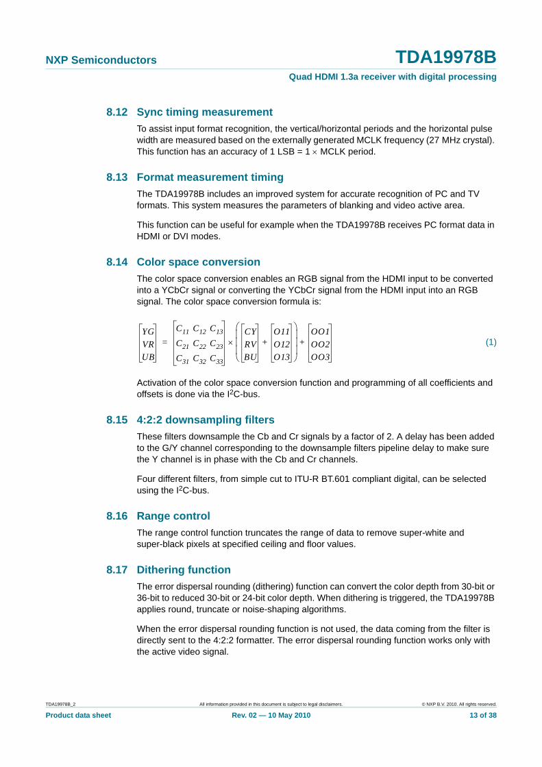
8.12 Sync timing measurementTo assist input format recognition, the vertical/horizontal periods and the horizontal pulse width are measured based on the externally generated MCLK frequency (27 MHz crystal). This function has an accuracy of 1 LSB = 1 × MCLK period.
8.13 Format measurement timingThe TDA19978B includes an improved system for accurate recognition of PC and TV formats. This system measures the parameters of blanking and video active area.
This function can be useful for example when the TDA19978B receives PC format data in HDMI or DVI modes.
8.14 Color space conversionThe color space conversion enables an RGB signal from the HDMI input to be converted into a YCbCr signal or converting the YCbCr signal from the HDMI input into an RGB signal. The color space conversion formula is:
(1)
Activation of the color space conversion function and programming of all coefficients and offsets is done via the I2C-bus.
8.15 4:2:2 downsampling filtersThese filters downsample the Cb and Cr signals by a factor of 2. A delay has been added to the G/Y channel corresponding to the downsample filters pipeline delay to make sure the Y channel is in phase with the Cb and Cr channels.
Four different filters, from simple cut to ITU-R BT.601 compliant digital, can be selected using the I2C-bus.
8.16 Range controlThe range control function truncates the range of data to remove super-white and super-black pixels at specified ceiling and floor values.
8.17 Dithering functionThe error dispersal rounding (dithering) function can convert the color depth from 30-bit or 36-bit to reduced 30-bit or 24-bit color depth. When dithering is triggered, the TDA19978B applies round, truncate or noise-shaping algorithms.
When the error dispersal rounding function is not used, the data coming from the filter is directly sent to the 4:2:2 formatter. The error dispersal rounding function works only with the active video signal.
YGVRUB
C11 C12 C13
C21 C22 C23
C31 C32 C33
CYRVBU
O11O12O13
+
⎝ ⎠⎜ ⎟⎜ ⎟⎜ ⎟⎛ ⎞
×OO1OO2OO3
+=
TDA19978B_2 All information provided in this document is subject to legal disclaimers. © NXP B.V. 2010. All rights reserved.
Product data sheet Rev. 02 — 10 May 2010 13 of 38
NXP Semiconductors TDA19978BQuad HDMI 1.3a receiver with digital processing
8.18 4:2:2 formatterThe 4:2:2 formatter contains the YCbCr 4:2:2 semi-planar and the YCbCr 4:2:2 ITU-R BT.656 formatting functions. The selection of these functions is made using the I2C-bus.
• In YCbCr 4:2:2 mode: the data frequency of the Y signal is equal to the pixel clock frequency. While the data frequency of the Cb and Cr signals is equal to half the pixel clock frequency
• In semi-planar mode: the output clock frequency should be the same as the pixel clock frequency
• In ITU-R BT.656 mode: the data frequency should be the same as the formatter clock frequency (e.g. pixel clock frequency × 2)
The Start Active Video (SAV) and End Active Video (EAV) timing reference codes can be included in the data stream based on the HREF, VREF and FREF positions from the VHREF timing generator.
Specific codes programmed using the I2C-bus can replace the data stream during the blanking period to mask gain and clamp calibration.
8.19 Video port selectionEach channel can be allocated to a specified video port using the I2C-bus (see Section 13 “Output video port formats (mapping examples)” on page 20) to optimize board layout at the interface with video processing ICs. For example:
• R, G or B in RGB 4:4:4 mode on pins VP[29:20]• Y, Cb or Cr in YUV 4:4:4 mode on pins VP[19:10]• Y or Cb-Cr in 4:2:2 semi-planar mode on pins VP[9:0]• Cb-Y-Cr-Y in 4:2:2 ITU-R BT.656 mode on pins VP[9:0]
Each video port can be set to high-impedance using the I2C-bus.
8.20 Output buffersThe output buffers are LV-TTL compatible. The outputs can be switched between active and high-impedance by the I2C-bus.
The outputs HREF, VREF and FREF can be set to high-impedance (Z) or forced LOW (L), independently of the timing reference codes.
8.21 VHREF timing generatorThe VHREF timing generator outputs all of the timing signals used by the device:
• VREF, HREF and FREF signals for SAV, EAV and active video area definition• VS and HS to change width and position compared with the HDMI inputs
8.22 I2C-bus serial interfaceThe I2C-bus serial interface enables the internal registers of the device to be programmed. The slave address of the device is selected by pin A0.
TDA19978B_2 All information provided in this document is subject to legal disclaimers. © NXP B.V. 2010. All rights reserved.
Product data sheet Rev. 02 — 10 May 2010 14 of 38
NXP Semiconductors TDA19978BQuad HDMI 1.3a receiver with digital processing
8.23 Power managementThe TDA19978B can use one of three Power-down modes:
• level 0: full Power-down mode• level 1: internal EDID memory with I2C-bus serial interface active• level 2: internal EDID memory with I2C-bus serial interface and activity detection
enabled
The user can activate each mode with pin PD or using I2C-bus registers:
• level 0: PD pin is HIGH• level 1: settings defined in the I2C-bus registers• level 2: settings defined in the I2C-bus registers
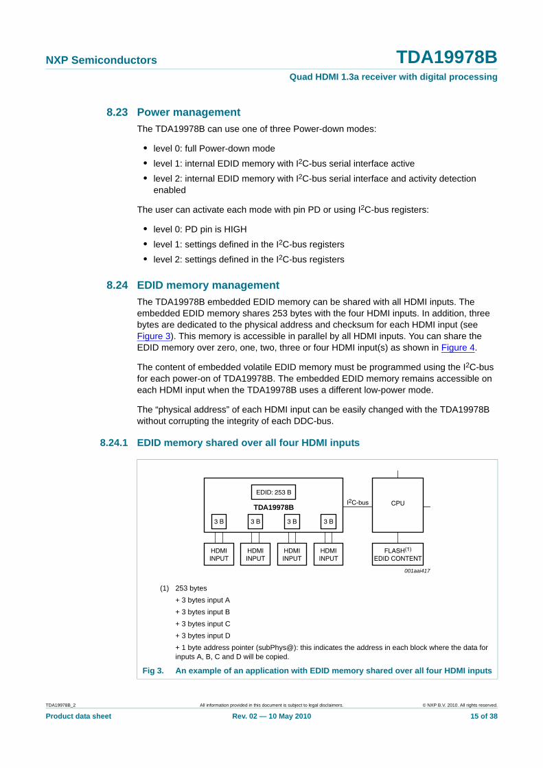
8.24 EDID memory managementThe TDA19978B embedded EDID memory can be shared with all HDMI inputs. The embedded EDID memory shares 253 bytes with the four HDMI inputs. In addition, three bytes are dedicated to the physical address and checksum for each HDMI input (see Figure 3). This memory is accessible in parallel by all HDMI inputs. You can share the EDID memory over zero, one, two, three or four HDMI input(s) as shown in Figure 4.
The content of embedded volatile EDID memory must be programmed using the I2C-bus for each power-on of TDA19978B. The embedded EDID memory remains accessible on each HDMI input when the TDA19978B uses a different low-power mode.
The “physical address” of each HDMI input can be easily changed with the TDA19978B without corrupting the integrity of each DDC-bus.
8.24.1 EDID memory shared over all four HDMI inputs
(1) 253 bytes+ 3 bytes input A+ 3 bytes input B+ 3 bytes input C+ 3 bytes input D+ 1 byte address pointer (subPhys@): this indicates the address in each block where the data for inputs A, B, C and D will be copied.
Fig 3. An example of an application with EDID memory shared over all four HDMI inputs
001aai417
EDID: 253 B
3 B
HDMIINPUT
I2C-bus CPU
FLASH(1)
EDID CONTENT
TDA19978B
3 B
HDMIINPUT
3 B
HDMIINPUT
3 B
HDMIINPUT
TDA19978B_2 All information provided in this document is subject to legal disclaimers. © NXP B.V. 2010. All rights reserved.
Product data sheet Rev. 02 — 10 May 2010 15 of 38
NXP Semiconductors TDA19978BQuad HDMI 1.3a receiver with digital processing
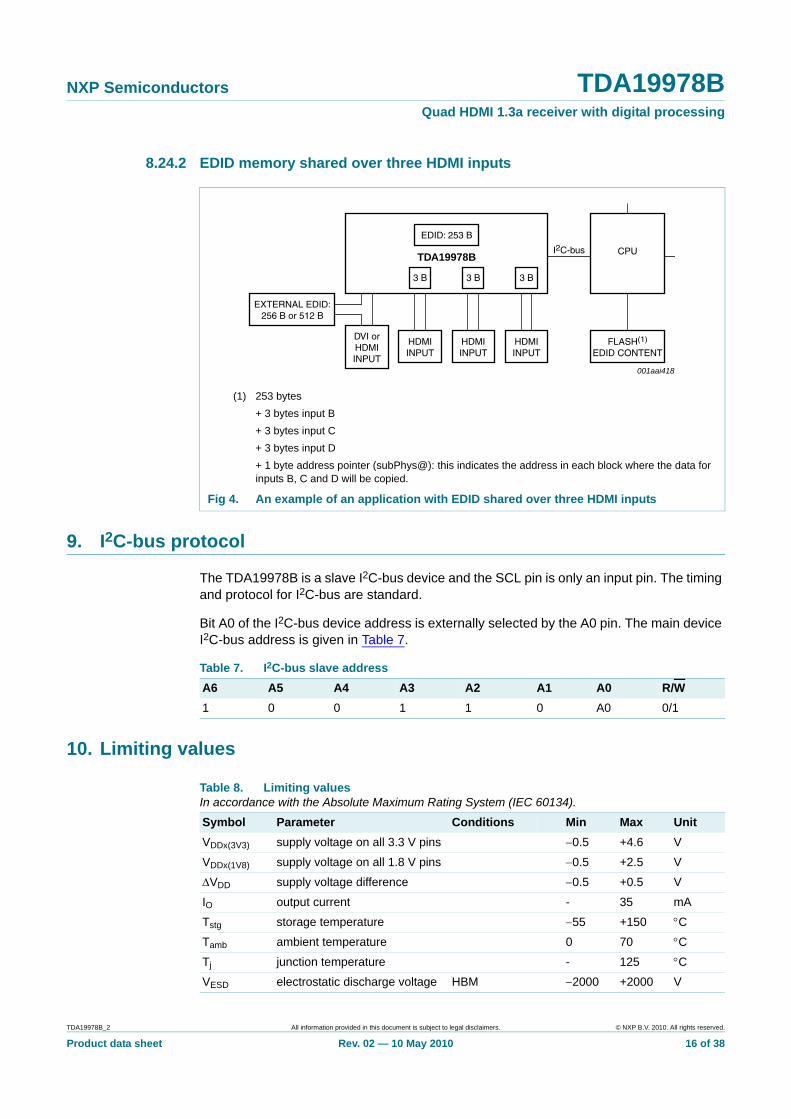
8.24.2 EDID memory shared over three HDMI inputs
9. I2C-bus protocol
The TDA19978B is a slave I2C-bus device and the SCL pin is only an input pin. The timing and protocol for I2C-bus are standard.
Bit A0 of the I2C-bus device address is externally selected by the A0 pin. The main device I2C-bus address is given in Table 7.
10. Limiting values
(1) 253 bytes+ 3 bytes input B+ 3 bytes input C+ 3 bytes input D+ 1 byte address pointer (subPhys@): this indicates the address in each block where the data for inputs B, C and D will be copied.
Fig 4. An example of an application with EDID shared over three HDMI inputs
001aai418
EDID: 253 B
EXTERNAL EDID:256 B or 512 B
DVI orHDMIINPUT
I2C-bus CPU
FLASH(1)
EDID CONTENT
TDA19978B
3 B
HDMIINPUT
3 B
HDMIINPUT
3 B
HDMIINPUT
Table 7. I2C-bus slave addressA6 A5 A4 A3 A2 A1 A0 R/W1 0 0 1 1 0 A0 0/1
Table 8. Limiting valuesIn accordance with the Absolute Maximum Rating System (IEC 60134).
Symbol Parameter Conditions Min Max UnitVDDx(3V3) supply voltage on all 3.3 V pins −0.5 +4.6 V
VDDx(1V8) supply voltage on all 1.8 V pins −0.5 +2.5 V
ΔVDD supply voltage difference −0.5 +0.5 V
IO output current - 35 mA
Tstg storage temperature −55 +150 °C
Tamb ambient temperature 0 70 °C
Tj junction temperature - 125 °C
VESD electrostatic discharge voltage HBM −2000 +2000 V
TDA19978B_2 All information provided in this document is subject to legal disclaimers. © NXP B.V. 2010. All rights reserved.
Product data sheet Rev. 02 — 10 May 2010 16 of 38
NXP Semiconductors TDA19978BQuad HDMI 1.3a receiver with digital processing
11. Thermal characteristics
12. Characteristics
Table 9. Thermal characteristicsSymbol Parameter Conditions Typ UnitRth(j-a) thermal resistance from junction to ambient in free air 22.8 K/W
Rth(j-c) thermal resistance from junction to case 11.1 K/W
Table 10. CharacteristicsTamb = 0 °C to 70 °C; typical values measured at Tamb = 25 °C; unless otherwise specified.
Symbol Parameter Conditions Min Typ Max UnitSuppliesVDDH(3V3) HDMI supply voltage (3.3 V) 3.135 3.3 3.465 V
VDDH(1V8) HDMI supply voltage (1.8 V) 1.71 1.8 1.89 V
VDDI(3V3) input supply voltage (3.3 V) 3.135 3.3 3.465 V
VDDC(1V8) core supply voltage (1.8 V) 1.71 1.8 1.89 V
VDDO(3V3) output supply voltage (3.3 V) 3.135 3.3 3.465 V
IDDH(3V3) HDMI supply current (3.3 V) 720p at 60 Hz [1] - 103 - mA
1080p at 60 Hz [1] - 106 - mA
1080p at 60 Hz; Deep Color mode [1] - 110 - mA
IDDH(1V8) HDMI supply current (1.8 V) 720p at 60 Hz [1] - 48 - mA
1080p at 60 Hz [1] - 68 - mA
1080p at 60 Hz; Deep Color mode [1] - 85 - mA
IDDI(3V3) input supply current (3.3 V) 720p at 60 Hz [1] - 1 - mA
1080p at 60 Hz [1] - 1 - mA
1080p at 60 Hz; Deep Color mode [1] - 1 - mA
IDDO(3V3) output supply current (3.3 V) 720p at 60 Hz [1] - 49 - mA
1080p at 60 Hz [1] - 78 - mA
1080p at 60 Hz; Deep Color mode [1] - 120 - mA
IDDC(1V8) core supply current (1.8 V) 720p at 60 Hz [1] - 148 - mA
1080p at 60 Hz [1] - 283 - mA
1080p at 60 Hz; Deep Color mode [1] - 453 - mA
ΔVDD(3V3-3V3) supply voltage difference between two 3.3 V supplies
start-up and established conditions −100 - +100 mV
ΔVDD(1V8-1V8) supply voltage difference between two 1.8 V supplies
start-up and established conditions −100 - +100 mV
P power dissipation Active mode [1]
720p at 60 Hz - 0.75 - W
1080p at 60 Hz - 1.13 - W
1080p at 60 Hz; Deep Color mode
- 1.63 - W
TDA19978B_2 All information provided in this document is subject to legal disclaimers. © NXP B.V. 2010. All rights reserved.
Product data sheet Rev. 02 — 10 May 2010 17 of 38

NXP Semiconductors TDA19978BQuad HDMI 1.3a receiver with digital processing
Pcons power consumption Power-down mode
pin PD = HIGH - 1 - mW
I2C-bus; EDID - 4 - mW
I2C-bus; EDID; activity detection - 150 - mW
Clock timing output: pins VCLK, ACLK and SYSCLKfclk(max) maximum clock frequency pin VCLK 165 - - MHz
pin ACLK 25 - - MHz
pin SYSCLK 50 - - MHz
δclk clock duty cycle pin VCLK - 50 - %
pin ACLK - 50 - %
pin SYSCLK - 50 - %
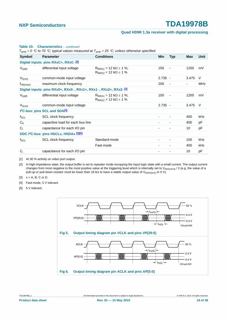
Timing output: pins VP[29:0]; fs = 165 MHz; CL = 10 pF; see Figure 5tsu(Q) data output set-up time 0.40 - 1.50 ns
th(Q) data output hold time 0.80 - 2.00 ns
td(pipe) pipeline delay time clock intervals from inputs to outputs; all modes
- 80 × Tclk -
Timing output: pins AP[5:0] with respect to pin ACLK; fclk = 12.288 MHz; CL = 10 pF; see Figure 6tsu(Q) data output set-up time 69 - - ns
th(Q) data output hold time 2 - - ns
LV-TTL digital outputs: pins VP[29:0], VCLK, AP[5:0], ACLK, DE, HS, VS, HREF, VREF, FREF; CL = 10 pFVOL LOW-level output voltage IOL = 2 mA - - 0.4 V
VOH HIGH-level output voltage IOH = −2 mA 2.4 - - V
ILOZ OFF-state output leakage current high-impedance state; VO = 0 V [2] - 0 - μA
VO = VDDO(3V3) × 1⁄3 10 - 100 μA
VO = VDDO(3V3) × 2⁄3 −100 - −10 μA
VO = VDDO(3V3) - 0 - μA
Table 10. Characteristics …continuedTamb = 0 °C to 70 °C; typical values measured at Tamb = 25 °C; unless otherwise specified.
Symbol Parameter Conditions Min Typ Max Unit
TDA19978B_2 All information provided in this document is subject to legal disclaimers. © NXP B.V. 2010. All rights reserved.
Product data sheet Rev. 02 — 10 May 2010 18 of 38
NXP Semiconductors TDA19978BQuad HDMI 1.3a receiver with digital processing
[1] At 30 % activity on video port output.
[2] In high-impedance state, the output buffer is set to repeater mode recopying the input logic state with a small current. The output current changes from most negative to the most positive value at the triggering level which is internally set to VDDO(3V3) / 2 (e.g. the value of a pull-up or pull-down resistor must be lower than 18 kΩ to have a stable output value of VDDO(3V3) or 0 V).
[3] x = A, B, C or D.
[4] Fast-mode, 5 V tolerant.
[5] 5 V tolerant.
Digital inputs: pins RXxC+, RXxC−[3]
VI(dif) differential input voltage RRRX1 = 12 kΩ ± 1 %; RRRX2 = 12 kΩ ± 1 %
150 - 1200 mV
VI(cm) common-mode input voltage 2.735 - 3.475 V
fclk(max) maximum clock frequency 205 - - MHz
Digital inputs: pins RXx0+, RXx0−, RXx1+, RXx1−, RXx2+, RXx2−[3]
VI(dif) differential input voltage RRRX1 = 12 kΩ ± 1 %; RRRX2 = 12 kΩ ± 1 %
150 - 1200 mV
VI(cm) common-mode input voltage 2.735 - 3.475 V
I2C-bus: pins SCL and SDA[4]
fSCL SCL clock frequency - - 400 kHz
Cb capacitive load for each bus line - - 400 pF
Ci capacitance for each I/O pin - - 10 pF
DDC I2C-bus: pins HSCLx, HSDAx [3][5]
fSCL SCL clock frequency Standard-mode - - 100 kHz
Fast-mode - - 400 kHz
Ci capacitance for each I/O pin - - 10 pF
Table 10. Characteristics …continuedTamb = 0 °C to 70 °C; typical values measured at Tamb = 25 °C; unless otherwise specified.
Symbol Parameter Conditions Min Typ Max Unit
Fig 5. Output timing diagram pin VCLK and pins VP[29:0]
Fig 6. Output timing diagram pin ACLK and pins AP[5:0]
001aah368
VCLK 50 %
2.4 V
0.4 VVP[29:0]
tsu(Q)
th(Q)
001aah369
ACLK 50 %
2.4 V
0.4 VAP[5:0]
tsu(Q)
th(Q)
TDA19978B_2 All information provided in this document is subject to legal disclaimers. © NXP B.V. 2010. All rights reserved.
Product data sheet Rev. 02 — 10 May 2010 19 of 38
NXP Semiconductors TDA19978BQuad HDMI 1.3a receiver with digital processing
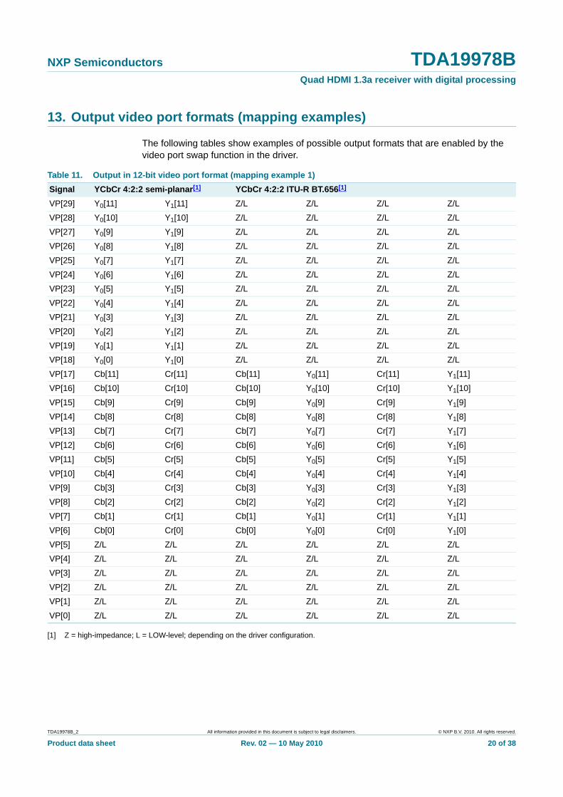
13. Output video port formats (mapping examples)
The following tables show examples of possible output formats that are enabled by the video port swap function in the driver.
[1] Z = high-impedance; L = LOW-level; depending on the driver configuration.
Table 11. Output in 12-bit video port format (mapping example 1)Signal YCbCr 4:2:2 semi-planar[1] YCbCr 4:2:2 ITU-R BT.656[1]
VP[29] Y0[11] Y1[11] Z/L Z/L Z/L Z/L
VP[28] Y0[10] Y1[10] Z/L Z/L Z/L Z/L
VP[27] Y0[9] Y1[9] Z/L Z/L Z/L Z/L
VP[26] Y0[8] Y1[8] Z/L Z/L Z/L Z/L
VP[25] Y0[7] Y1[7] Z/L Z/L Z/L Z/L
VP[24] Y0[6] Y1[6] Z/L Z/L Z/L Z/L
VP[23] Y0[5] Y1[5] Z/L Z/L Z/L Z/L
VP[22] Y0[4] Y1[4] Z/L Z/L Z/L Z/L
VP[21] Y0[3] Y1[3] Z/L Z/L Z/L Z/L
VP[20] Y0[2] Y1[2] Z/L Z/L Z/L Z/L
VP[19] Y0[1] Y1[1] Z/L Z/L Z/L Z/L
VP[18] Y0[0] Y1[0] Z/L Z/L Z/L Z/L
VP[17] Cb[11] Cr[11] Cb[11] Y0[11] Cr[11] Y1[11]
VP[16] Cb[10] Cr[10] Cb[10] Y0[10] Cr[10] Y1[10]
VP[15] Cb[9] Cr[9] Cb[9] Y0[9] Cr[9] Y1[9]
VP[14] Cb[8] Cr[8] Cb[8] Y0[8] Cr[8] Y1[8]
VP[13] Cb[7] Cr[7] Cb[7] Y0[7] Cr[7] Y1[7]
VP[12] Cb[6] Cr[6] Cb[6] Y0[6] Cr[6] Y1[6]
VP[11] Cb[5] Cr[5] Cb[5] Y0[5] Cr[5] Y1[5]
VP[10] Cb[4] Cr[4] Cb[4] Y0[4] Cr[4] Y1[4]
VP[9] Cb[3] Cr[3] Cb[3] Y0[3] Cr[3] Y1[3]
VP[8] Cb[2] Cr[2] Cb[2] Y0[2] Cr[2] Y1[2]
VP[7] Cb[1] Cr[1] Cb[1] Y0[1] Cr[1] Y1[1]
VP[6] Cb[0] Cr[0] Cb[0] Y0[0] Cr[0] Y1[0]
VP[5] Z/L Z/L Z/L Z/L Z/L Z/L
VP[4] Z/L Z/L Z/L Z/L Z/L Z/L
VP[3] Z/L Z/L Z/L Z/L Z/L Z/L
VP[2] Z/L Z/L Z/L Z/L Z/L Z/L
VP[1] Z/L Z/L Z/L Z/L Z/L Z/L
VP[0] Z/L Z/L Z/L Z/L Z/L Z/L
TDA19978B_2 All information provided in this document is subject to legal disclaimers. © NXP B.V. 2010. All rights reserved.
Product data sheet Rev. 02 — 10 May 2010 20 of 38
NXP Semiconductors TDA19978BQuad HDMI 1.3a receiver with digital processing
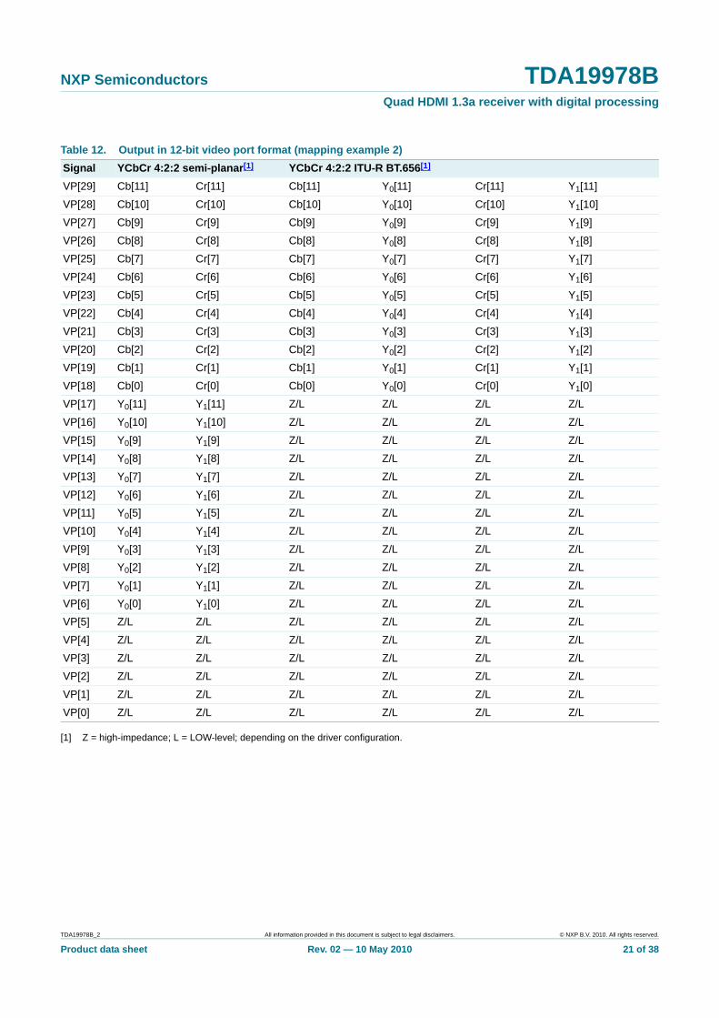
[1] Z = high-impedance; L = LOW-level; depending on the driver configuration.
Table 12. Output in 12-bit video port format (mapping example 2)Signal YCbCr 4:2:2 semi-planar[1] YCbCr 4:2:2 ITU-R BT.656[1]
VP[29] Cb[11] Cr[11] Cb[11] Y0[11] Cr[11] Y1[11]
VP[28] Cb[10] Cr[10] Cb[10] Y0[10] Cr[10] Y1[10]
VP[27] Cb[9] Cr[9] Cb[9] Y0[9] Cr[9] Y1[9]
VP[26] Cb[8] Cr[8] Cb[8] Y0[8] Cr[8] Y1[8]
VP[25] Cb[7] Cr[7] Cb[7] Y0[7] Cr[7] Y1[7]
VP[24] Cb[6] Cr[6] Cb[6] Y0[6] Cr[6] Y1[6]
VP[23] Cb[5] Cr[5] Cb[5] Y0[5] Cr[5] Y1[5]
VP[22] Cb[4] Cr[4] Cb[4] Y0[4] Cr[4] Y1[4]
VP[21] Cb[3] Cr[3] Cb[3] Y0[3] Cr[3] Y1[3]
VP[20] Cb[2] Cr[2] Cb[2] Y0[2] Cr[2] Y1[2]
VP[19] Cb[1] Cr[1] Cb[1] Y0[1] Cr[1] Y1[1]
VP[18] Cb[0] Cr[0] Cb[0] Y0[0] Cr[0] Y1[0]
VP[17] Y0[11] Y1[11] Z/L Z/L Z/L Z/L
VP[16] Y0[10] Y1[10] Z/L Z/L Z/L Z/L
VP[15] Y0[9] Y1[9] Z/L Z/L Z/L Z/L
VP[14] Y0[8] Y1[8] Z/L Z/L Z/L Z/L
VP[13] Y0[7] Y1[7] Z/L Z/L Z/L Z/L
VP[12] Y0[6] Y1[6] Z/L Z/L Z/L Z/L
VP[11] Y0[5] Y1[5] Z/L Z/L Z/L Z/L
VP[10] Y0[4] Y1[4] Z/L Z/L Z/L Z/L
VP[9] Y0[3] Y1[3] Z/L Z/L Z/L Z/L
VP[8] Y0[2] Y1[2] Z/L Z/L Z/L Z/L
VP[7] Y0[1] Y1[1] Z/L Z/L Z/L Z/L
VP[6] Y0[0] Y1[0] Z/L Z/L Z/L Z/L
VP[5] Z/L Z/L Z/L Z/L Z/L Z/L
VP[4] Z/L Z/L Z/L Z/L Z/L Z/L
VP[3] Z/L Z/L Z/L Z/L Z/L Z/L
VP[2] Z/L Z/L Z/L Z/L Z/L Z/L
VP[1] Z/L Z/L Z/L Z/L Z/L Z/L
VP[0] Z/L Z/L Z/L Z/L Z/L Z/L
TDA19978B_2 All information provided in this document is subject to legal disclaimers. © NXP B.V. 2010. All rights reserved.
Product data sheet Rev. 02 — 10 May 2010 21 of 38
NXP Semiconductors TDA19978BQuad HDMI 1.3a receiver with digital processing
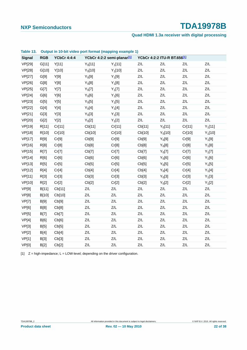
[1] Z = high-impedance; L = LOW-level; depending on the driver configuration.
Table 13. Output in 10-bit video port format (mapping example 1)Signal RGB YCbCr 4:4:4 YCbCr 4:2:2 semi-planar[1] YCbCr 4:2:2 ITU-R BT.656[1]
VP[29] G[11] Y[11] Y0[11] Y1[11] Z/L Z/L Z/L Z/L
VP[28] G[10] Y[10] Y0[10] Y1[10] Z/L Z/L Z/L Z/L
VP[27] G[9] Y[9] Y0[9] Y1[9] Z/L Z/L Z/L Z/L
VP[26] G[8] Y[8] Y0[8] Y1[8] Z/L Z/L Z/L Z/L
VP[25] G[7] Y[7] Y0[7] Y1[7] Z/L Z/L Z/L Z/L
VP[24] G[6] Y[6] Y0[6] Y1[6] Z/L Z/L Z/L Z/L
VP[23] G[5] Y[5] Y0[5] Y1[5] Z/L Z/L Z/L Z/L
VP[22] G[4] Y[4] Y0[4] Y1[4] Z/L Z/L Z/L Z/L
VP[21] G[3] Y[3] Y0[3] Y1[3] Z/L Z/L Z/L Z/L
VP[20] G[2] Y[2] Y0[2] Y1[2] Z/L Z/L Z/L Z/L
VP[19] R[11] Cr[11] Cb[11] Cr[11] Cb[11] Y0[11] Cr[11] Y1[11]
VP[18] R[10] Cr[10] Cb[10] Cr[10] Cb[10] Y0[10] Cr[10] Y1[10]
VP[17] R[9] Cr[9] Cb[9] Cr[9] Cb[9] Y0[9] Cr[9] Y1[9]
VP[16] R[8] Cr[8] Cb[8] Cr[8] Cb[8] Y0[8] Cr[8] Y1[8]
VP[15] R[7] Cr[7] Cb[7] Cr[7] Cb[7] Y0[7] Cr[7] Y1[7]
VP[14] R[6] Cr[6] Cb[6] Cr[6] Cb[6] Y0[6] Cr[6] Y1[6]
VP[13] R[5] Cr[5] Cb[5] Cr[5] Cb[5] Y0[5] Cr[5] Y1[5]
VP[12] R[4] Cr[4] Cb[4] Cr[4] Cb[4] Y0[4] Cr[4] Y1[4]
VP[11] R[3] Cr[3] Cb[3] Cr[3] Cb[3] Y0[3] Cr[3] Y1[3]
VP[10] R[2] Cr[2] Cb[2] Cr[2] Cb[2] Y0[2] Cr[2] Y1[2]
VP[9] B[11] Cb[11] Z/L Z/L Z/L Z/L Z/L Z/L
VP[8] B[10] Cb[10] Z/L Z/L Z/L Z/L Z/L Z/L
VP[7] B[9] Cb[9] Z/L Z/L Z/L Z/L Z/L Z/L
VP[6] B[8] Cb[8] Z/L Z/L Z/L Z/L Z/L Z/L
VP[5] B[7] Cb[7] Z/L Z/L Z/L Z/L Z/L Z/L
VP[4] B[6] Cb[6] Z/L Z/L Z/L Z/L Z/L Z/L
VP[3] B[5] Cb[5] Z/L Z/L Z/L Z/L Z/L Z/L
VP[2] B[4] Cb[4] Z/L Z/L Z/L Z/L Z/L Z/L
VP[1] B[3] Cb[3] Z/L Z/L Z/L Z/L Z/L Z/L
VP[0] B[2] Cb[2] Z/L Z/L Z/L Z/L Z/L Z/L
TDA19978B_2 All information provided in this document is subject to legal disclaimers. © NXP B.V. 2010. All rights reserved.
Product data sheet Rev. 02 — 10 May 2010 22 of 38

NXP Semiconductors TDA19978BQuad HDMI 1.3a receiver with digital processing
[1] Z = high-impedance; L = LOW-level; depending on the driver configuration.
Table 14. Output in 10-bit video port format (mapping example 2)Signal RGB YCbCr 4:4:4 YCbCr 4:2:2 semi-planar[1] YCbCr 4:2:2 ITU-R BT.656[1]
VP[29] B[11] Cb[11] Z/L Z/L Z/L Z/L Z/L Z/L
VP[28] B[10] Cb[10] Z/L Z/L Z/L Z/L Z/L Z/L
VP[27] B[9] Cb[9] Z/L Z/L Z/L Z/L Z/L Z/L
VP[26] B[8] Cb[8] Z/L Z/L Z/L Z/L Z/L Z/L
VP[25] B[7] Cb[7] Z/L Z/L Z/L Z/L Z/L Z/L
VP[24] B[6] Cb[6] Z/L Z/L Z/L Z/L Z/L Z/L
VP[23] B[5] Cb[5] Z/L Z/L Z/L Z/L Z/L Z/L
VP[22] B[4] Cb[4] Z/L Z/L Z/L Z/L Z/L Z/L
VP[21] B[3] Cb[3] Z/L Z/L Z/L Z/L Z/L Z/L
VP[20] B[2] Cb[2] Z/L Z/L Z/L Z/L Z/L Z/L
VP[19] G[11] Y[11] Y0[11] Y1[11] Z/L Z/L Z/L Z/L
VP[18] G[10] Y[10] Y0[10] Y1[10] Z/L Z/L Z/L Z/L
VP[17] G[9] Y[9] Y0[9] Y1[9] Z/L Z/L Z/L Z/L
VP[16] G[8] Y[8] Y0[8] Y1[8] Z/L Z/L Z/L Z/L
VP[15] G[7] Y[7] Y0[7] Y1[7] Z/L Z/L Z/L Z/L
VP[14] G[6] Y[6] Y0[6] Y1[6] Z/L Z/L Z/L Z/L
VP[13] G[5] Y[5] Y0[5] Y1[5] Z/L Z/L Z/L Z/L
VP[12] G[4] Y[4] Y0[4] Y1[4] Z/L Z/L Z/L Z/L
VP[11] G[3] Y[3] Y0[3] Y1[3] Z/L Z/L Z/L Z/L
VP[10] G[2] Y[2] Y0[2] Y1[2] Z/L Z/L Z/L Z/L
VP[9] R[11] Cr[11] Cb[11] Cr[11] Cb[11] Y0[11] Cr[11] Y1[11]
VP[8] R[10] Cr[10] Cb[10] Cr[10] Cb[10] Y0[10] Cr[10] Y1[10]
VP[7] R[9] Cr[9] Cb[9] Cr[9] Cb[9] Y0[9] Cr[9] Y1[9]
VP[6] R[8] Cr[8] Cb[8] Cr[8] Cb[8] Y0[8] Cr[8] Y1[8]
VP[5] R[7] Cr[7] Cb[7] Cr[7] Cb[7] Y0[7] Cr[7] Y1[7]
VP[4] R[6] Cr[6] Cb[6] Cr[6] Cb[6] Y0[6] Cr[6] Y1[6]
VP[3] R[5] Cr[5] Cb[5] Cr[5] Cb[5] Y0[5] Cr[5] Y1[5]
VP[2] R[4] Cr[4] Cb[4] Cr[4] Cb[4] Y0[4] Cr[4] Y1[4]
VP[1] R[3] Cr[3] Cb[3] Cr[3] Cb[3] Y0[3] Cr[3] Y1[3]
VP[0] R[2] Cr[2] Cb[2] Cr[2] Cb[2] Y0[2] Cr[2] Y1[2]
TDA19978B_2 All information provided in this document is subject to legal disclaimers. © NXP B.V. 2010. All rights reserved.
Product data sheet Rev. 02 — 10 May 2010 23 of 38
NXP Semiconductors TDA19978BQuad HDMI 1.3a receiver with digital processing
[1] Z = high-impedance; L = LOW-level; depending on the driver configuration.
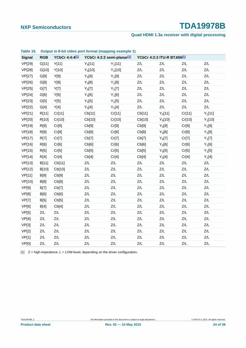
Table 15. Output in 8-bit video port format (mapping example 1)Signal RGB YCbCr 4:4:4[1] YCbCr 4:2:2 semi-planar[1] YCbCr 4:2:2 ITU-R BT.656[1]
VP[29] G[11] Y[11] Y0[11] Y1[11] Z/L Z/L Z/L Z/L
VP[28] G[10] Y[10] Y0[10] Y1[10] Z/L Z/L Z/L Z/L
VP[27] G[9] Y[9] Y0[9] Y1[9] Z/L Z/L Z/L Z/L
VP[26] G[8] Y[8] Y0[8] Y1[8] Z/L Z/L Z/L Z/L
VP[25] G[7] Y[7] Y0[7] Y1[7] Z/L Z/L Z/L Z/L
VP[24] G[6] Y[6] Y0[6] Y1[6] Z/L Z/L Z/L Z/L
VP[23] G[5] Y[5] Y0[5] Y1[5] Z/L Z/L Z/L Z/L
VP[22] G[4] Y[4] Y0[4] Y1[4] Z/L Z/L Z/L Z/L
VP[21] R[11] Cr[11] Cb[11] Cr[11] Cb[11] Y0[11] Cr[11] Y1[11]
VP[20] R[10] Cr[10] Cb[10] Cr[10] Cb[10] Y0[10] Cr[10] Y1[10]
VP[19] R[9] Cr[9] Cb[9] Cr[9] Cb[9] Y0[9] Cr[9] Y1[9]
VP[18] R[8] Cr[8] Cb[8] Cr[8] Cb[8] Y0[8] Cr[8] Y1[8]
VP[17] R[7] Cr[7] Cb[7] Cr[7] Cb[7] Y0[7] Cr[7] Y1[7]
VP[16] R[6] Cr[6] Cb[6] Cr[6] Cb[6] Y0[6] Cr[6] Y1[6]
VP[15] R[5] Cr[5] Cb[5] Cr[5] Cb[5] Y0[5] Cr[5] Y1[5]
VP[14] R[4] Cr[4] Cb[4] Cr[4] Cb[4] Y0[4] Cr[4] Y1[4]
VP[13] B[11] Cb[11] Z/L Z/L Z/L Z/L Z/L Z/L
VP[12] B[10] Cb[10] Z/L Z/L Z/L Z/L Z/L Z/L
VP[11] B[9] Cb[9] Z/L Z/L Z/L Z/L Z/L Z/L
VP[10] B[8] Cb[8] Z/L Z/L Z/L Z/L Z/L Z/L
VP[9] B[7] Cb[7] Z/L Z/L Z/L Z/L Z/L Z/L
VP[8] B[6] Cb[6] Z/L Z/L Z/L Z/L Z/L Z/L
VP[7] B[5] Cb[5] Z/L Z/L Z/L Z/L Z/L Z/L
VP[6] B[4] Cb[4] Z/L Z/L Z/L Z/L Z/L Z/L
VP[5] Z/L Z/L Z/L Z/L Z/L Z/L Z/L Z/L
VP[4] Z/L Z/L Z/L Z/L Z/L Z/L Z/L Z/L
VP[3] Z/L Z/L Z/L Z/L Z/L Z/L Z/L Z/L
VP[2] Z/L Z/L Z/L Z/L Z/L Z/L Z/L Z/L
VP[1] Z/L Z/L Z/L Z/L Z/L Z/L Z/L Z/L
VP[0] Z/L Z/L Z/L Z/L Z/L Z/L Z/L Z/L
TDA19978B_2 All information provided in this document is subject to legal disclaimers. © NXP B.V. 2010. All rights reserved.
Product data sheet Rev. 02 — 10 May 2010 24 of 38
NXP Semiconductors TDA19978BQuad HDMI 1.3a receiver with digital processing
[1] Z = high-impedance; L = LOW-level; depending on the driver configuration.
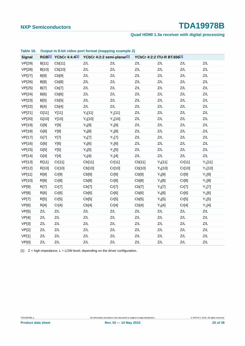
Table 16. Output in 8-bit video port format (mapping example 2)Signal RGB[1] YCbCr 4:4:4[1] YCbCr 4:2:2 semi-planar[1] YCbCr 4:2:2 ITU-R BT.656[1]
VP[29] B[11] Cb[11] Z/L Z/L Z/L Z/L Z/L Z/L
VP[28] B[10] Cb[10] Z/L Z/L Z/L Z/L Z/L Z/L
VP[27] B[9] Cb[9] Z/L Z/L Z/L Z/L Z/L Z/L
VP[26] B[8] Cb[8] Z/L Z/L Z/L Z/L Z/L Z/L
VP[25] B[7] Cb[7] Z/L Z/L Z/L Z/L Z/L Z/L
VP[24] B[6] Cb[6] Z/L Z/L Z/L Z/L Z/L Z/L
VP[23] B[5] Cb[5] Z/L Z/L Z/L Z/L Z/L Z/L
VP[22] B[4] Cb[4] Z/L Z/L Z/L Z/L Z/L Z/L
VP[21] G[11] Y[11] Y0[11] Y1[11] Z/L Z/L Z/L Z/L
VP[20] G[10] Y[10] Y0[10] Y1[10] Z/L Z/L Z/L Z/L
VP[19] G[9] Y[9] Y0[9] Y1[9] Z/L Z/L Z/L Z/L
VP[18] G[8] Y[8] Y0[8] Y1[8] Z/L Z/L Z/L Z/L
VP[17] G[7] Y[7] Y0[7] Y1[7] Z/L Z/L Z/L Z/L
VP[16] G[6] Y[6] Y0[6] Y1[6] Z/L Z/L Z/L Z/L
VP[15] G[5] Y[5] Y0[5] Y1[5] Z/L Z/L Z/L Z/L
VP[14] G[4] Y[4] Y0[4] Y1[4] Z/L Z/L Z/L Z/L
VP[13] R[11] Cr[11] Cb[11] Cr[11] Cb[11] Y0[11] Cr[11] Y1[11]
VP[12] R[10] Cr[10] Cb[10] Cr[10] Cb[10] Y0[10] Cr[10] Y1[10]
VP[11] R[9] Cr[9] Cb[9] Cr[9] Cb[9] Y0[9] Cr[9] Y1[9]
VP[10] R[8] Cr[8] Cb[8] Cr[8] Cb[8] Y0[8] Cr[8] Y1[8]
VP[9] R[7] Cr[7] Cb[7] Cr[7] Cb[7] Y0[7] Cr[7] Y1[7]
VP[8] R[6] Cr[6] Cb[6] Cr[6] Cb[6] Y0[6] Cr[6] Y1[6]
VP[7] R[5] Cr[5] Cb[5] Cr[5] Cb[5] Y0[5] Cr[5] Y1[5]
VP[6] R[4] Cr[4] Cb[4] Cr[4] Cb[4] Y0[4] Cr[4] Y1[4]
VP[5] Z/L Z/L Z/L Z/L Z/L Z/L Z/L Z/L
VP[4] Z/L Z/L Z/L Z/L Z/L Z/L Z/L Z/L
VP[3] Z/L Z/L Z/L Z/L Z/L Z/L Z/L Z/L
VP[2] Z/L Z/L Z/L Z/L Z/L Z/L Z/L Z/L
VP[1] Z/L Z/L Z/L Z/L Z/L Z/L Z/L Z/L
VP[0] Z/L Z/L Z/L Z/L Z/L Z/L Z/L Z/L
TDA19978B_2 All information provided in this document is subject to legal disclaimers. © NXP B.V. 2010. All rights reserved.
Product data sheet Rev. 02 — 10 May 2010 25 of 38
NXP Semiconductors TDA19978BQuad HDMI 1.3a receiver with digital processing
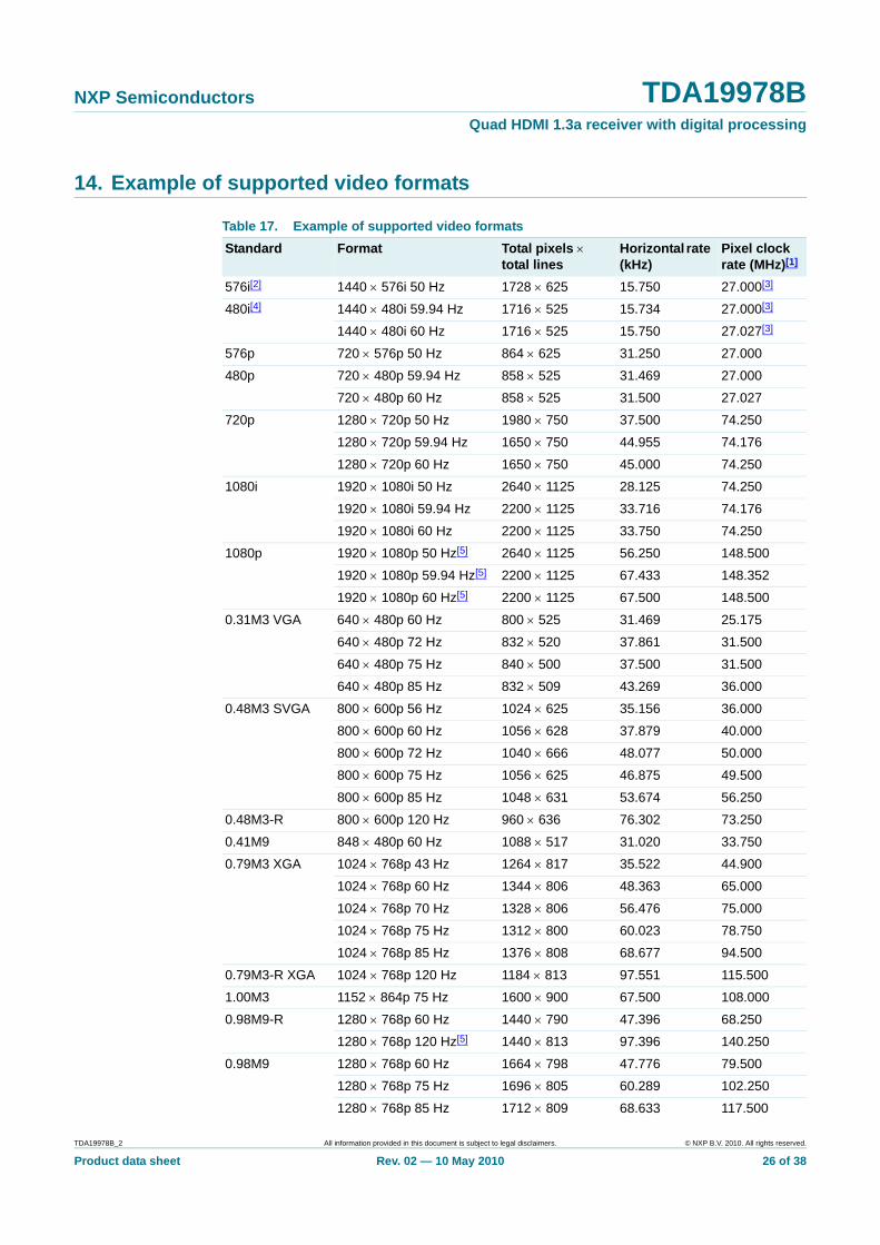
14. Example of supported video formats
Table 17. Example of supported video formatsStandard Format Total pixels ×
total linesHorizontal rate (kHz)
Pixel clock rate (MHz)[1]
576i[2] 1440 × 576i 50 Hz 1728 × 625 15.750 27.000[3]
480i[4] 1440 × 480i 59.94 Hz 1716 × 525 15.734 27.000[3]
1440 × 480i 60 Hz 1716 × 525 15.750 27.027[3]
576p 720 × 576p 50 Hz 864 × 625 31.250 27.000
480p 720 × 480p 59.94 Hz 858 × 525 31.469 27.000
720 × 480p 60 Hz 858 × 525 31.500 27.027
720p 1280 × 720p 50 Hz 1980 × 750 37.500 74.250
1280 × 720p 59.94 Hz 1650 × 750 44.955 74.176
1280 × 720p 60 Hz 1650 × 750 45.000 74.250
1080i 1920 × 1080i 50 Hz 2640 × 1125 28.125 74.250
1920 × 1080i 59.94 Hz 2200 × 1125 33.716 74.176
1920 × 1080i 60 Hz 2200 × 1125 33.750 74.250
1080p 1920 × 1080p 50 Hz[5] 2640 × 1125 56.250 148.500
1920 × 1080p 59.94 Hz[5] 2200 × 1125 67.433 148.352
1920 × 1080p 60 Hz[5] 2200 × 1125 67.500 148.500
0.31M3 VGA 640 × 480p 60 Hz 800 × 525 31.469 25.175
640 × 480p 72 Hz 832 × 520 37.861 31.500
640 × 480p 75 Hz 840 × 500 37.500 31.500
640 × 480p 85 Hz 832 × 509 43.269 36.000
0.48M3 SVGA 800 × 600p 56 Hz 1024 × 625 35.156 36.000
800 × 600p 60 Hz 1056 × 628 37.879 40.000
800 × 600p 72 Hz 1040 × 666 48.077 50.000
800 × 600p 75 Hz 1056 × 625 46.875 49.500
800 × 600p 85 Hz 1048 × 631 53.674 56.250
0.48M3-R 800 × 600p 120 Hz 960 × 636 76.302 73.250
0.41M9 848 × 480p 60 Hz 1088 × 517 31.020 33.750
0.79M3 XGA 1024 × 768p 43 Hz 1264 × 817 35.522 44.900
1024 × 768p 60 Hz 1344 × 806 48.363 65.000
1024 × 768p 70 Hz 1328 × 806 56.476 75.000
1024 × 768p 75 Hz 1312 × 800 60.023 78.750
1024 × 768p 85 Hz 1376 × 808 68.677 94.500
0.79M3-R XGA 1024 × 768p 120 Hz 1184 × 813 97.551 115.500
1.00M3 1152 × 864p 75 Hz 1600 × 900 67.500 108.000
0.98M9-R 1280 × 768p 60 Hz 1440 × 790 47.396 68.250
1280 × 768p 120 Hz[5] 1440 × 813 97.396 140.250
0.98M9 1280 × 768p 60 Hz 1664 × 798 47.776 79.500
1280 × 768p 75 Hz 1696 × 805 60.289 102.250
1280 × 768p 85 Hz 1712 × 809 68.633 117.500
TDA19978B_2 All information provided in this document is subject to legal disclaimers. © NXP B.V. 2010. All rights reserved.
Product data sheet Rev. 02 — 10 May 2010 26 of 38

NXP Semiconductors TDA19978BQuad HDMI 1.3a receiver with digital processing
[1] Pixel clock rate corresponds to VCLK output for 4:4:4 format and 4:2:2 semi-planar; VCLK / 2 for 4:2:2 ITU-R BT.656 format. The pixel clock rate can be determined by:a) Total pixels × total lines × frame rate for the progressive format.b) Total pixels × total lines × frame rate / 2 for the interlaced format.
[2] Also referred to as PAL (Phase Alternating Line).
[3] Pixel-doubling.
[4] Also referred to as NTSC (National Television Standards Committee).
[5] Only supports Deep Color mode 10-bit.
[6] Sometimes also referred to as WUXGA (Wide Ultra eXtended Graphics Array).
1.02MA-R 1280 × 800p 60 Hz 1440 × 823 49.306 71.000
1280 × 800p 120 Hz[5] 1440 × 847 101.563 146.250
1.02MA 1280 × 800p 60 Hz 1680 × 831 49.702 83.500
1280 × 800p 75 Hz 1696 × 838 62.795 106.500
1280 × 800p 85 Hz 1712 × 843 71.554 122.500
1.23M3 1280 × 960p 60 Hz 1800 × 1000 60.000 108.000
1280 × 960p 85 Hz[5] 1728 × 1011 85.938 148.500
1.31M4 SXGA 1280 × 1024p 60 Hz 1688 × 1066 63.981 108.000
1280 × 1024p 75 Hz 1688 × 1066 79.976 135.000
1280 × 1024p 85 Hz[5] 1728 × 1072 91.146 157.500
1.04M9 1360 × 768p 60 Hz 1792 × 795 47.712 85.500
1.04M9-R 1360 × 768p 120 Hz[5] 1520 × 813 97.533 148.250
1.47M3-R 1400 × 1050p 60 Hz 1560 × 1080 64.744 101.000
1.47M3 1400 × 1050p 60 Hz 1864 × 1089 65.317 121.750
1400 × 1050p 75 Hz[5] 1896 × 1099 82.278 156.000
1.29MA-R 1440 × 900p 60 Hz 1600 × 926 55.469 88.750
1.29MA 1440 × 900p 60 Hz 1904 × 934 55.935 106.500
1440 × 900p 75 Hz[5] 1936 × 942 70.635 136.750
1440 × 900p 85 Hz[5] 1952 × 948 80.430 157.000
1.92M3 UXGA 1600 × 1200p 60 Hz[5] 2160 × 1250 75.000 162.000
1.76MA-R 1680 × 1050p 60 Hz 1840 × 1080 64.674 119.000
1.76MA 1680 × 1050p 60 Hz[5] 2240 × 1089 65.290 146.250
2.30MA-R[6] 1920 × 1200p 60 Hz[5] 2080 × 1235 74.038 154.000
Table 17. Example of supported video formats …continued
Standard Format Total pixels × total lines
Horizontal rate (kHz)
Pixel clock rate (MHz)[1]
TDA19978B_2 All information provided in this document is subject to legal disclaimers. © NXP B.V. 2010. All rights reserved.
Product data sheet Rev. 02 — 10 May 2010 27 of 38
NXP Semiconductors TDA19978BQuad HDMI 1.3a receiver with digital processing
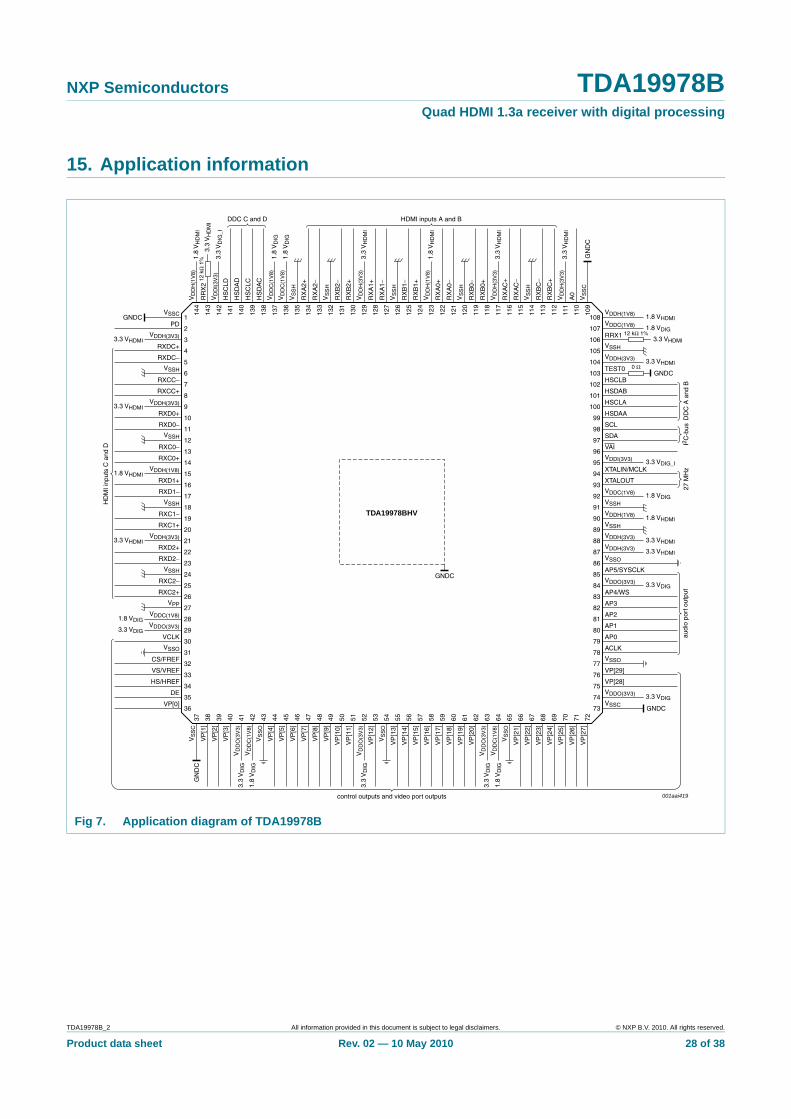
15. Application information
Fig 7. Application diagram of TDA19978B
001aai419
0 Ω
12 kΩ 1%
VSSC1081
VDDH(1V8)
TDA19978BHV
PD1072
VDDC(1V8)
VDDH(3V3)3.3 VHDMI
3.3 VHDMI
1.8 VDIG
3.3 VDIG
1.8
VD
IG
3.3
VD
IG
1.8
VD
IG
3.3
VD
IG
3.3 VDIG
3.3 VDIG
3.3 VHDMI
3.3 VHDMI
3.3 VHDMI
3.3 VHDMI
12 k
Ω 1
%3.
3 V
HD
MI
1.8
VH
DM
I
3.3
VH
DM
I
3.3
VH
DM
I
3.3
VH
DM
I
1.8
VH
DM
I
1.8
VD
IG
3.3
VD
IG_I
1.8
VD
IG
1.8 VHDMI
1.8 VDIG
1.8 VHDMI
1.8 VDIG
3.3 VDIG_I
3.3
VD
IG
3.3 VHDMI
1.8 VHDMI
1063RRX1
RXDC+1054
VSSH
RXDC−1045
VDDH(3V3)
VSSH1036
TEST0
RXCC−1027
HSCLB
RXCC+1018
HSDAB
VDDH(3V3)1009
HSCLA
RXD0+9910
HSDAA
RXD0−9811
SCL
VSSH9712
SDA
RXC0−9613
VAI
RXC0+9514
VDDI(3V3)
VDDH(1V8)9415
XTALIN/MCLK
RXD1+9316
XTALOUT
RXD1−9217
VDDC(1V8)
VSSH9118
VSSH
RXC1−9019
VDDH(1V8)
RXC1+8920
VSSH
VDDH(3V3)8821
VDDH(3V3)
RXD2+8722
VDDH(3V3)
RXD2−8623
VSSO
VSSH8524
AP5/SYSCLK
RXC2−8425
VDDO(3V3)
RXC2+8326
AP4/WS
VPP8227
AP3
GNDC
GNDC
GNDC
GNDC
GN
DC
GN
DC
VDDC(1V8)8128
AP2
VDDO(3V3)8029
AP1
VCLK7930
AP0
VSSO7831
ACLK
CS/FREF7732
VSSO
VS/VREF7633
VP[29]
HS/HREF7534
VP[28]
DE7435
VDDO(3V3)
VP[0]7336
VSSC
VS
SC
144
37V
DD
H(1
V8)
VP
[1]
143
38R
RX
2
VP
[2]
142
39V
DD
I(3V
3)
VP
[3]
141
40H
SC
LD
HD
MI i
nput
s C
and
D
HDMI inputs A and B
control outputs and video port outputs
DDC C and D
I2C
-bus
27 M
Hz
DD
C A
and
Bau
dio
port
out
put
VD
DO
(3V
3)14
041
HS
DA
D
VD
DC
(1V
8)13
942
HS
CLC
VS
SO
138
43H
SD
AC
VP
[4]
137
44V
DD
C(1
V8)
VP
[5]
136
45V
DD
C(1
V8)
VP
[6]
135
46V
SS
H
VP
[7]
134
47R
XA
2+
VP
[8]
133
48R
XA
2−
VP
[9]
132
49V
SS
H
VP
[10]
131
50R
XB
2−
VP
[11]
130
51R
XB
2+
VD
DO
(3V
3)12
952
VD
DH
(3V
3)
VP
[12]
128
53R
XA
1+
VS
SO
127
54R
XA
1−
VP
[13]
126
55V
SS
H
VP
[14]
125
56R
XB
1−
VP
[15]
124
57R
XB
1+
VP
[16]
123
58V
DD
H(1
V8)
VP
[17]
122
59R
XA
0+
VP
[18]
121
60R
XA
0−
VP
[19]
120
61V
SS
H
VP
[20]
119
62R
XB
0−V
DD
O(3
V3)
118
63R
XB
0+
VD
DC
(1V
8)11
764
VD
DH
(3V
3)
VS
SO
116
65R
XA
C+
VP
[21]
115
66R
XA
C−
VP
[22]
114
67V
SS
H
VP
[23]
113
68R
XB
C−
VP
[24]
112
69R
XB
C+
VP
[25]
111
70V
DD
H(3
V3)
VP
[26]
110
71A
0
VP
[27]
109
72V
SS
C
TDA19978B_2 All information provided in this document is subject to legal disclaimers. © NXP B.V. 2010. All rights reserved.
Product data sheet Rev. 02 — 10 May 2010 28 of 38
NXP Semiconductors TDA19978BQuad HDMI 1.3a receiver with digital processing
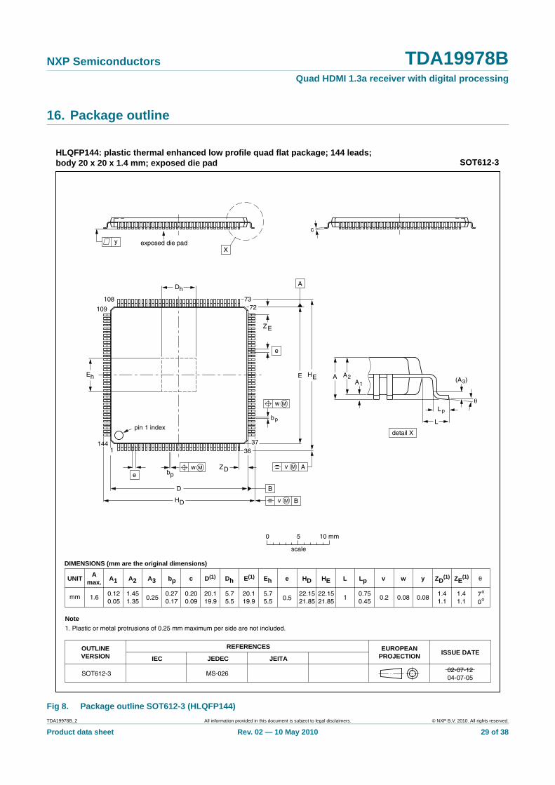
16. Package outline
Fig 8. Package outline SOT612-3 (HLQFP144)
UNIT A1 A2 A3 bp c e HEHD L Lp ZE(1)ZD
(1)ywv θ
REFERENCESOUTLINEVERSION
EUROPEANPROJECTION ISSUE DATE
IEC JEDEC JEITA
mm 0.120.05
1.451.35
0.250.270.17
0.200.09
20.119.9 0.5
22.1521.85
1.41.1
70
o
o0.080.2 0.081
DIMENSIONS (mm are the original dimensions)
Note
1. Plastic or metal protrusions of 0.25 mm maximum per side are not included.
0.750.45
SOT612-3 MS-026 02-07-1204-07-05
D(1) E(1)
20.119.9
Dh
5.75.5
Eh
5.75.5
22.1521.85
1.41.1
0 5 10 mm
scale
bpe
θ
EA1
A
Lp
detail X
L
(A )3
B
c
bp
EH A2
DH v M B
D
ZD
A
ZE
e
v M A
Xy
w M
w M
Amax.
1.6
HLQFP144: plastic thermal enhanced low profile quad flat package; 144 leads;body 20 x 20 x 1.4 mm; exposed die pad SOT612-3
108
109
pin 1 index
Eh
Dh
exposed die pad
7372
371
14436
TDA19978B_2 All information provided in this document is subject to legal disclaimers. © NXP B.V. 2010. All rights reserved.
Product data sheet Rev. 02 — 10 May 2010 29 of 38
NXP Semiconductors TDA19978BQuad HDMI 1.3a receiver with digital processing
17. Soldering of SMD packages
This text provides a very brief insight into a complex technology. A more in-depth account of soldering ICs can be found in Application Note AN10365 “Surface mount reflow soldering description”.
17.1 Introduction to solderingSoldering is one of the most common methods through which packages are attached to Printed Circuit Boards (PCBs), to form electrical circuits. The soldered joint provides both the mechanical and the electrical connection. There is no single soldering method that is ideal for all IC packages. Wave soldering is often preferred when through-hole and Surface Mount Devices (SMDs) are mixed on one printed wiring board; however, it is not suitable for fine pitch SMDs. Reflow soldering is ideal for the small pitches and high densities that come with increased miniaturization.
17.2 Wave and reflow solderingWave soldering is a joining technology in which the joints are made by solder coming from a standing wave of liquid solder. The wave soldering process is suitable for the following:
• Through-hole components• Leaded or leadless SMDs, which are glued to the surface of the printed circuit board
Not all SMDs can be wave soldered. Packages with solder balls, and some leadless packages which have solder lands underneath the body, cannot be wave soldered. Also, leaded SMDs with leads having a pitch smaller than ~0.6 mm cannot be wave soldered, due to an increased probability of bridging.
The reflow soldering process involves applying solder paste to a board, followed by component placement and exposure to a temperature profile. Leaded packages, packages with solder balls, and leadless packages are all reflow solderable.
Key characteristics in both wave and reflow soldering are:
• Board specifications, including the board finish, solder masks and vias• Package footprints, including solder thieves and orientation• The moisture sensitivity level of the packages• Package placement• Inspection and repair• Lead-free soldering versus SnPb soldering
17.3 Wave solderingKey characteristics in wave soldering are:
• Process issues, such as application of adhesive and flux, clinching of leads, board transport, the solder wave parameters, and the time during which components are exposed to the wave
• Solder bath specifications, including temperature and impurities
TDA19978B_2 All information provided in this document is subject to legal disclaimers. © NXP B.V. 2010. All rights reserved.
Product data sheet Rev. 02 — 10 May 2010 30 of 38
NXP Semiconductors TDA19978BQuad HDMI 1.3a receiver with digital processing
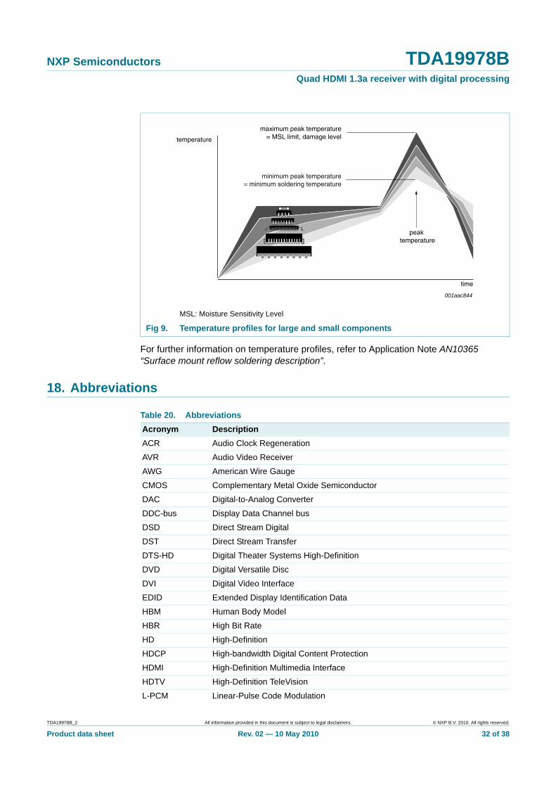
17.4 Reflow solderingKey characteristics in reflow soldering are:
• Lead-free versus SnPb soldering; note that a lead-free reflow process usually leads to higher minimum peak temperatures (see Figure 9) than a SnPb process, thus reducing the process window
• Solder paste printing issues including smearing, release, and adjusting the process window for a mix of large and small components on one board
• Reflow temperature profile; this profile includes preheat, reflow (in which the board is heated to the peak temperature) and cooling down. It is imperative that the peak temperature is high enough for the solder to make reliable solder joints (a solder paste characteristic). In addition, the peak temperature must be low enough that the packages and/or boards are not damaged. The peak temperature of the package depends on package thickness and volume and is classified in accordance with Table 18 and 19
Moisture sensitivity precautions, as indicated on the packing, must be respected at all times.
Studies have shown that small packages reach higher temperatures during reflow soldering, see Figure 9.
Table 18. SnPb eutectic process (from J-STD-020C)Package thickness (mm) Package reflow temperature (°C)
Volume (mm3)< 350 ≥ 350
< 2.5 235 220
≥ 2.5 220 220
Table 19. Lead-free process (from J-STD-020C)Package thickness (mm) Package reflow temperature (°C)
Volume (mm3)< 350 350 to 2000 > 2000
< 1.6 260 260 260
1.6 to 2.5 260 250 245
> 2.5 250 245 245
TDA19978B_2 All information provided in this document is subject to legal disclaimers. © NXP B.V. 2010. All rights reserved.
Product data sheet Rev. 02 — 10 May 2010 31 of 38
NXP Semiconductors TDA19978BQuad HDMI 1.3a receiver with digital processing
For further information on temperature profiles, refer to Application Note AN10365 “Surface mount reflow soldering description”.
18. Abbreviations
MSL: Moisture Sensitivity Level
Fig 9. Temperature profiles for large and small components
001aac844
temperature
time
minimum peak temperature= minimum soldering temperature
maximum peak temperature= MSL limit, damage level
peak temperature
Table 20. AbbreviationsAcronym DescriptionACR Audio Clock Regeneration
AVR Audio Video Receiver
AWG American Wire Gauge
CMOS Complementary Metal Oxide Semiconductor
DAC Digital-to-Analog Converter
DDC-bus Display Data Channel bus
DSD Direct Stream Digital
DST Direct Stream Transfer
DTS-HD Digital Theater Systems High-Definition
DVD Digital Versatile Disc
DVI Digital Video Interface
EDID Extended Display Identification Data
HBM Human Body Model
HBR High Bit Rate
HD High-Definition
HDCP High-bandwidth Digital Content Protection
HDMI High-Definition Multimedia Interface
HDTV High-Definition TeleVision
L-PCM Linear-Pulse Code Modulation
TDA19978B_2 All information provided in this document is subject to legal disclaimers. © NXP B.V. 2010. All rights reserved.
Product data sheet Rev. 02 — 10 May 2010 32 of 38
NXP Semiconductors TDA19978BQuad HDMI 1.3a receiver with digital processing
19. Revision history
LSB Least Significant Bit
LV-TTL Low Voltage Transistor-Transistor Logic
NTSC National Television Standards Committee
OBA One Bit Audio
OTP One Time Programmable
PAL Phase Alternating Line
PLL Phase-Locked Loop
RGB Red Green Blue
SACD Super Audio CD
SVGA Super Video Graphics Array
SXGA Super eXtended Graphics Array
S/PDIF Sony/Philips Digital Interface Format
TMDS Transition Minimized Differential Signaling
UXGA Ultra eXtended Graphics Array
VGA Video Graphics Array
WUXGA Wide Ultra eXtended Graphics Array
XGA eXtended Graphics Array
YCbCr Y = Luminance, Cb = Chroma blue, Cr = Chroma red
YUV Y = Luminance, U and V are chrominance signals
Table 20. Abbreviations …continued
Acronym Description
Table 21. Revision historyDocument ID Release date Data sheet status Change notice SupersedesTDA19978B_2 20100510 Product data sheet - TDA19978B_1
Modifications: • Section 1 “General description”: replaced 2.25 gigasamples per second by 2.05 gigasamples per second
• Section 1 “General description”: updated the Deep Color mode in 12-bit• Section 2 “Features and benefits”: replaced 225 MHz by 205 MHz• Table 1 “Quick reference data”: updated• Section 8.5 “Activity detection”: replaced 225 MHz by 205 MHz• Table 10 “Characteristics”: updated• Table 17 “Example of supported video formats”: updated
TDA19978B_1 20080807 Product data sheet - -
TDA19978B_2 All information provided in this document is subject to legal disclaimers. © NXP B.V. 2010. All rights reserved.
Product data sheet Rev. 02 — 10 May 2010 33 of 38
NXP Semiconductors TDA19978BQuad HDMI 1.3a receiver with digital processing
20. Legal information
20.1 Data sheet status
[1] Please consult the most recently issued document before initiating or completing a design.
[2] The term ‘short data sheet’ is explained in section “Definitions”.
[3] The product status of device(s) described in this document may have changed since this document was published and may differ in case of multiple devices. The latest product status information is available on the Internet at URL http://www.nxp.com.
20.2 DefinitionsDraft — The document is a draft version only. The content is still under internal review and subject to formal approval, which may result in modifications or additions. NXP Semiconductors does not give any representations or warranties as to the accuracy or completeness of information included herein and shall have no liability for the consequences of use of such information.
Short data sheet — A short data sheet is an extract from a full data sheet with the same product type number(s) and title. A short data sheet is intended for quick reference only and should not be relied upon to contain detailed and full information. For detailed and full information see the relevant full data sheet, which is available on request via the local NXP Semiconductors sales office. In case of any inconsistency or conflict with the short data sheet, the full data sheet shall prevail.
Product specification — The information and data provided in a Product data sheet shall define the specification of the product as agreed between NXP Semiconductors and its customer, unless NXP Semiconductors and customer have explicitly agreed otherwise in writing. In no event however, shall an agreement be valid in which the NXP Semiconductors product is deemed to offer functions and qualities beyond those described in the Product data sheet.
20.3 DisclaimersLimited warranty and liability — Information in this document is believed to be accurate and reliable. However, NXP Semiconductors does not give any representations or warranties, expressed or implied, as to the accuracy or completeness of such information and shall have no liability for the consequences of use of such information.
In no event shall NXP Semiconductors be liable for any indirect, incidental, punitive, special or consequential damages (including - without limitation - lost profits, lost savings, business interruption, costs related to the removal or replacement of any products or rework charges) whether or not such damages are based on tort (including negligence), warranty, breach of contract or any other legal theory.
Notwithstanding any damages that customer might incur for any reason whatsoever, NXP Semiconductors’ aggregate and cumulative liability towards customer for the products described herein shall be limited in accordance with the Terms and conditions of commercial sale of NXP Semiconductors.
Right to make changes — NXP Semiconductors reserves the right to make changes to information published in this document, including without limitation specifications and product descriptions, at any time and without notice. This document supersedes and replaces all information supplied prior to the publication hereof.
Suitability for use — NXP Semiconductors products are not designed, authorized or warranted to be suitable for use in life support, life-critical or safety-critical systems or equipment, nor in applications where failure or
malfunction of an NXP Semiconductors product can reasonably be expected to result in personal injury, death or severe property or environmental damage. NXP Semiconductors accepts no liability for inclusion and/or use of NXP Semiconductors products in such equipment or applications and therefore such inclusion and/or use is at the customer’s own risk.
Applications — Applications that are described herein for any of these products are for illustrative purposes only. NXP Semiconductors makes no representation or warranty that such applications will be suitable for the specified use without further testing or modification.
Customers are responsible for the design and operation of their applications and products using NXP Semiconductors products, and NXP Semiconductors accepts no liability for any assistance with applications or customer product design. It is customer’s sole responsibility to determine whether the NXP Semiconductors product is suitable and fit for the customer’s applications and products planned, as well as for the planned application and use of customer’s third party customer(s). Customers should provide appropriate design and operating safeguards to minimize the risks associated with their applications and products.
NXP Semiconductors does not accept any liability related to any default, damage, costs or problem which is based on any weakness or default in the customer’s applications or products, or the application or use by customer’s third party customer(s). Customer is responsible for doing all necessary testing for the customer’s applications and products using NXP Semiconductors products in order to avoid a default of the applications and the products or of the application or use by customer’s third party customer(s). NXP does not accept any liability in this respect.
Limiting values — Stress above one or more limiting values (as defined in the Absolute Maximum Ratings System of IEC 60134) will cause permanent damage to the device. Limiting values are stress ratings only and (proper) operation of the device at these or any other conditions above those given in the Recommended operating conditions section (if present) or the Characteristics sections of this document is not warranted. Constant or repeated exposure to limiting values will permanently and irreversibly affect the quality and reliability of the device.
Terms and conditions of commercial sale — NXP Semiconductors products are sold subject to the general terms and conditions of commercial sale, as published at http://www.nxp.com/profile/terms, unless otherwise agreed in a valid written individual agreement. In case an individual agreement is concluded only the terms and conditions of the respective agreement shall apply. NXP Semiconductors hereby expressly objects to applying the customer’s general terms and conditions with regard to the purchase of NXP Semiconductors products by customer.
No offer to sell or license — Nothing in this document may be interpreted or construed as an offer to sell products that is open for acceptance or the grant, conveyance or implication of any license under any copyrights, patents or other industrial or intellectual property rights.
Export control — This document as well as the item(s) described herein may be subject to export control regulations. Export might require a prior authorization from national authorities.
Document status[1][2] Product status[3] Definition
Objective [short] data sheet Development This document contains data from the objective specification for product development.
Preliminary [short] data sheet Qualification This document contains data from the preliminary specification.
Product [short] data sheet Production This document contains the product specification.
TDA19978B_2 All information provided in this document is subject to legal disclaimers. © NXP B.V. 2010. All rights reserved.
Product data sheet Rev. 02 — 10 May 2010 34 of 38
NXP Semiconductors TDA19978BQuad HDMI 1.3a receiver with digital processing
Quick reference data — The Quick reference data is an extract of the product data given in the Limiting values and Characteristics sections of this document, and as such is not complete, exhaustive or legally binding.
Non-automotive qualified products — Unless this data sheet expressly states that this specific NXP Semiconductors product is automotive qualified, the product is not suitable for automotive use. It is neither qualified nor tested in accordance with automotive testing or application requirements. NXP Semiconductors accepts no liability for inclusion and/or use of non-automotive qualified products in automotive equipment or applications.
In the event that customer uses the product for design-in and use in automotive applications to automotive specifications and standards, customer (a) shall use the product without NXP Semiconductors’ warranty of the product for such automotive applications, use and specifications, and (b) whenever customer uses the product for automotive applications beyond NXP Semiconductors’ specifications such use shall be solely at customer’s own risk, and (c) customer fully indemnifies NXP Semiconductors for any liability, damages or failed product claims resulting from customer design and use of the product for automotive applications beyond NXP Semiconductors’ standard warranty and NXP Semiconductors’ product specifications.
20.4 Licenses
20.5 TrademarksNotice: All referenced brands, product names, service names and trademarks are the property of their respective owners.
I2C-bus — logo is a trademark of NXP B.V.
21. Contact information
For more information, please visit: http://www.nxp.com
For sales office addresses, please send an email to: [email protected]
Purchase of NXP ICs with HDMI technology
Use of an NXP IC with HDMI technology in equipment that complies with the HDMI standard requires a license from HDMI Licensing LLC, 1060 E. Arques Avenue Suite 100, Sunnyvale CA 94085, USA, e-mail: [email protected].
TDA19978B_2 All information provided in this document is subject to legal disclaimers. © NXP B.V. 2010. All rights reserved.
Product data sheet Rev. 02 — 10 May 2010 35 of 38
NXP Semiconductors TDA19978BQuad HDMI 1.3a receiver with digital processing
22. Tables
Table 1. Quick reference data . . . . . . . . . . . . . . . . . . . . .3Table 2. Ordering information . . . . . . . . . . . . . . . . . . . . .3Table 3. Pin description . . . . . . . . . . . . . . . . . . . . . . . . . .5Table 4. Audio port configuration (Layout 0) . . . . . . . . .12Table 5. Audio port configuration (Layout 1) . . . . . . . . .12Table 6. Audio port configuration for HBR and DST
packets . . . . . . . . . . . . . . . . . . . . . . . . . . . . . .12Table 7. I2C-bus slave address . . . . . . . . . . . . . . . . . . .16Table 8. Limiting values . . . . . . . . . . . . . . . . . . . . . . . . .16Table 9. Thermal characteristics . . . . . . . . . . . . . . . . . .17Table 10. Characteristics . . . . . . . . . . . . . . . . . . . . . . . . .17Table 11. Output in 12-bit video port format (mapping
example 1) . . . . . . . . . . . . . . . . . . . . . . . . . . . .20Table 12. Output in 12-bit video port format (mapping
example 2) . . . . . . . . . . . . . . . . . . . . . . . . . . . .21Table 13. Output in 10-bit video port format (mapping
example 1) . . . . . . . . . . . . . . . . . . . . . . . . . . . .22Table 14. Output in 10-bit video port format (mapping
example 2) . . . . . . . . . . . . . . . . . . . . . . . . . . . .23Table 15. Output in 8-bit video port format (mapping
example 1) . . . . . . . . . . . . . . . . . . . . . . . . . . . .24Table 16. Output in 8-bit video port format (mapping
example 2) . . . . . . . . . . . . . . . . . . . . . . . . . . . .25Table 17. Example of supported video formats . . . . . . . .26Table 18. SnPb eutectic process (from J-STD-020C) . . .31Table 19. Lead-free process (from J-STD-020C) . . . . . .31Table 20. Abbreviations . . . . . . . . . . . . . . . . . . . . . . . . . .32Table 21. Revision history . . . . . . . . . . . . . . . . . . . . . . . .33
TDA19978B_2 All information provided in this document is subject to legal disclaimers. © NXP B.V. 2010. All rights reserved.
Product data sheet Rev. 02 — 10 May 2010 36 of 38

NXP Semiconductors TDA19978BQuad HDMI 1.3a receiver with digital processing
23. Figures
Fig 1. Block diagram of TDA19978B . . . . . . . . . . . . . . . .4Fig 2. Pin configuration for TDA19978B . . . . . . . . . . . . .5Fig 3. An example of an application with EDID memory
shared over all four HDMI inputs . . . . . . . . . . . . .15Fig 4. An example of an application with EDID shared
over three HDMI inputs . . . . . . . . . . . . . . . . . . . .16Fig 5. Output timing diagram pin VCLK and pins
VP[29:0] . . . . . . . . . . . . . . . . . . . . . . . . . . . . . . . .19Fig 6. Output timing diagram pin ACLK and pins
AP[5:0] . . . . . . . . . . . . . . . . . . . . . . . . . . . . . . . . .19Fig 7. Application diagram of TDA19978B. . . . . . . . . . .28Fig 8. Package outline SOT612-3 (HLQFP144) . . . . . .29Fig 9. Temperature profiles for large and small
components . . . . . . . . . . . . . . . . . . . . . . . . . . . . .32
TDA19978B_2 All information provided in this document is subject to legal disclaimers. © NXP B.V. 2010. All rights reserved.
Product data sheet Rev. 02 — 10 May 2010 37 of 38
NXP Semiconductors TDA19978BQuad HDMI 1.3a receiver with digital processing
24. Contents
1 General description . . . . . . . . . . . . . . . . . . . . . . 12 Features and benefits . . . . . . . . . . . . . . . . . . . . 23 Applications . . . . . . . . . . . . . . . . . . . . . . . . . . . . 34 Quick reference data . . . . . . . . . . . . . . . . . . . . . 35 Ordering information. . . . . . . . . . . . . . . . . . . . . 36 Block diagram . . . . . . . . . . . . . . . . . . . . . . . . . . 47 Pinning information. . . . . . . . . . . . . . . . . . . . . . 57.1 Pinning . . . . . . . . . . . . . . . . . . . . . . . . . . . . . . . 57.2 Pin description . . . . . . . . . . . . . . . . . . . . . . . . . 58 Functional description . . . . . . . . . . . . . . . . . . . 98.1 Software drivers . . . . . . . . . . . . . . . . . . . . . . . . 98.2 HDMI inputs . . . . . . . . . . . . . . . . . . . . . . . . . . . 98.3 Termination resistance control . . . . . . . . . . . . . 98.4 Equalizer. . . . . . . . . . . . . . . . . . . . . . . . . . . . . 108.5 Activity detection. . . . . . . . . . . . . . . . . . . . . . . 108.6 Color depth unpacking . . . . . . . . . . . . . . . . . . 108.7 Derepeater . . . . . . . . . . . . . . . . . . . . . . . . . . . 108.8 Upsample . . . . . . . . . . . . . . . . . . . . . . . . . . . . 108.9 Packet extraction . . . . . . . . . . . . . . . . . . . . . . 108.10 Audio PLL . . . . . . . . . . . . . . . . . . . . . . . . . . . . 118.11 Audio formatter . . . . . . . . . . . . . . . . . . . . . . . . 118.12 Sync timing measurement . . . . . . . . . . . . . . . 138.13 Format measurement timing. . . . . . . . . . . . . . 138.14 Color space conversion . . . . . . . . . . . . . . . . . 138.15 4:2:2 downsampling filters . . . . . . . . . . . . . . . 138.16 Range control . . . . . . . . . . . . . . . . . . . . . . . . . 138.17 Dithering function . . . . . . . . . . . . . . . . . . . . . . 138.18 4:2:2 formatter . . . . . . . . . . . . . . . . . . . . . . . . 148.19 Video port selection . . . . . . . . . . . . . . . . . . . . 148.20 Output buffers . . . . . . . . . . . . . . . . . . . . . . . . . 148.21 VHREF timing generator . . . . . . . . . . . . . . . . 148.22 I2C-bus serial interface . . . . . . . . . . . . . . . . . . 148.23 Power management . . . . . . . . . . . . . . . . . . . . 158.24 EDID memory management . . . . . . . . . . . . . . 158.24.1 EDID memory shared over all four HDMI
inputs . . . . . . . . . . . . . . . . . . . . . . . . . . . . . . . 158.24.2 EDID memory shared over three HDMI
inputs . . . . . . . . . . . . . . . . . . . . . . . . . . . . . . . 169 I2C-bus protocol. . . . . . . . . . . . . . . . . . . . . . . . 1610 Limiting values. . . . . . . . . . . . . . . . . . . . . . . . . 1611 Thermal characteristics . . . . . . . . . . . . . . . . . 1712 Characteristics. . . . . . . . . . . . . . . . . . . . . . . . . 1713 Output video port formats
(mapping examples) . . . . . . . . . . . . . . . . . . . . 2014 Example of supported video formats. . . . . . . 26
15 Application information . . . . . . . . . . . . . . . . . 2816 Package outline. . . . . . . . . . . . . . . . . . . . . . . . 2917 Soldering of SMD packages. . . . . . . . . . . . . . 3017.1 Introduction to soldering. . . . . . . . . . . . . . . . . 3017.2 Wave and reflow soldering. . . . . . . . . . . . . . . 3017.3 Wave soldering . . . . . . . . . . . . . . . . . . . . . . . 3017.4 Reflow soldering . . . . . . . . . . . . . . . . . . . . . . 3118 Abbreviations . . . . . . . . . . . . . . . . . . . . . . . . . 3219 Revision history . . . . . . . . . . . . . . . . . . . . . . . 3320 Legal information . . . . . . . . . . . . . . . . . . . . . . 3420.1 Data sheet status . . . . . . . . . . . . . . . . . . . . . . 3420.2 Definitions . . . . . . . . . . . . . . . . . . . . . . . . . . . 3420.3 Disclaimers . . . . . . . . . . . . . . . . . . . . . . . . . . 3420.4 Licenses. . . . . . . . . . . . . . . . . . . . . . . . . . . . . 3520.5 Trademarks . . . . . . . . . . . . . . . . . . . . . . . . . . 3521 Contact information . . . . . . . . . . . . . . . . . . . . 3522 Tables . . . . . . . . . . . . . . . . . . . . . . . . . . . . . . . . 3623 Figures . . . . . . . . . . . . . . . . . . . . . . . . . . . . . . . 3724 Contents. . . . . . . . . . . . . . . . . . . . . . . . . . . . . . 38
© NXP B.V. 2010. All rights reserved.For more information, please visit: http://www.nxp.comFor sales office addresses, please send an email to: [email protected]
Date of release: 10 May 2010Document identifier: TDA19978B_2
Please be aware that important notices concerning this document and the product(s)described herein, have been included in section ‘Legal information’.