1 final year project development of method for improving the light-load efficiency of vrm’s...
TRANSCRIPT

11
Final Year ProjectFinal Year Project
Development of method for improving the Development of method for improving the light-load efficiency of VRM’slight-load efficiency of VRM’s
Project Project Supervisor :Supervisor :Dr. Maeve DuffyDr. Maeve DuffyMarch 2009March 2009

22
VRMVRM
Voltage Regulator ModuleVoltage Regulator Module Switching Mode Power Supply for MicroprocessorSwitching Mode Power Supply for Microprocessor The most suitable topography for a VRM The most suitable topography for a VRM
is a Multiphase Synchronous Buck Converteris a Multiphase Synchronous Buck Converter

33
Microprocessor Light Microprocessor Light LoadLoad
Power States Power States Optimize the runtime power consumptionOptimize the runtime power consumption
Sleep States Sleep States Idle Power ManagementsIdle Power Managements

44
Trends in VRM Design Trends in VRM Design is Microprocessor is Microprocessor LoadsLoads Moore’s Law will apply into the future - IntelMoore’s Law will apply into the future - Intel Lower core voltages and higher currents Lower core voltages and higher currents Analysis of recent VRM guideline from IntelAnalysis of recent VRM guideline from Intel
Design Design Guideline Guideline
VRM 9.1 VRM 9.1 VRM 10.0 VRM 10.0 VRM 11.0 VRM 11.0
Release Release DateDate
20022002 20052005 20082008
IccIcc 75A75A 85A85A 130A130A
Icc(max)Icc(max) 81A81A 100A100A 150A150A
Icc(step)Icc(step) 54A54A 70A70A 100A100A
dIcc/dtdIcc/dt 450A/uS450A/uS 560A/uS560A/uS 1200A/uS1200A/uS
VIDVID 1.1-1.85V 1.1-1.85V 0.8375 - 1.6V 0.8375 - 1.6V 0.5 - 1.6V 0.5 - 1.6V

55
Synchronous Buck Synchronous Buck Converter EfficiencyConverter Efficiency
Sources of Losses in the power stageSources of Losses in the power stage Upper and Lower MOSFET sUpper and Lower MOSFET s Output InductorOutput Inductor Output CapacitorOutput Capacitor
Cout RLoad
L11 2

66
Analysis of MOSFET Analysis of MOSFET LossesLosses
Conduction for Losses for Upper Conduction for Losses for Upper and Lower MOSFET sand Lower MOSFET s
Switching Losses for Upper MOSFETSwitching Losses for Upper MOSFET Lower MOSFET Body Diode conduction lossesLower MOSFET Body Diode conduction losses Reverse Recovery Losses Reverse Recovery Losses Gate Driver LossesGate Driver Losses

77
Capacitor and Inductor Capacitor and Inductor Losses Losses
Inductor LossesInductor Losses DCR and ACRDCR and ACR Hysteresis LossesHysteresis Losses Eddy Current LossesEddy Current Losses
Capacitor LossesCapacitor Losses ESR (Equivalent Series Resistance)ESR (Equivalent Series Resistance)

88
SPICE Modelling of SPICE Modelling of Power LossesPower LossesObjective is to use SPICE to measure MOSFET Objective is to use SPICE to measure MOSFET
switching losses from the instantaneous switching losses from the instantaneous products of current and voltageproducts of current and voltage
T
avg dttitvT
P0
)()(1

99
Shoot Through during Shoot Through during Upper MOSFET Switch OnUpper MOSFET Switch On
Time
493.0us 493.1us 493.2us 493.3us 493.4us 493.5us 493.6us 493.7us 493.8us 493.9us 494.0usI(U11:D) I(U13:D)
-20A
-10A
0A
10A
20A
30A
40A
50A
Time
493.0us 493.1us 493.2us 493.3us 493.4us 493.5us 493.6us 493.7us 493.8us 493.9us 494.0usI(U11:D) I(U13:D)
-20A
-10A
0A
10A
20A
30A
40A
50A
Drain Source CurrentDrain Source Current
Upper ONUpper ON Upper OFFUpper OFF
Upper ONUpper ON Upper OFFUpper OFF
1010
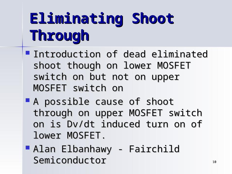
Eliminating Shoot Eliminating Shoot ThroughThrough
Introduction of dead eliminated Introduction of dead eliminated shoot though on lower MOSFET shoot though on lower MOSFET switch on but not on upper MOSFET switch on but not on upper MOSFET switch onswitch on
A possible cause of shoot through A possible cause of shoot through on upper MOSFET switch on is Dv/dt on upper MOSFET switch on is Dv/dt induced turn on of lower MOSFET.induced turn on of lower MOSFET.
Alan Elbanhawy - Fairchild Alan Elbanhawy - Fairchild SemiconductorSemiconductor

1111
Dv/dt Induced Turn On Dv/dt Induced Turn On of Lower MOSFETof Lower MOSFET
dt
tdvCti
)()(

1212
MathCAD Efficiency MathCAD Efficiency CalculatorCalculator
MathCAD displays equation and expression in MathCAD displays equation and expression in graphically form, and is aware of SI units.graphically form, and is aware of SI units.Easier to track calculations in MathCADEasier to track calculations in MathCAD
Used a MathCAD worksheet to calculate the Used a MathCAD worksheet to calculate the efficiency of a single phase of a synchronous buck efficiency of a single phase of a synchronous buck converterconverter
The original MathCAD worksheet was a The original MathCAD worksheet was a supplement to a paper called supplement to a paper called “What MOSFET Can “What MOSFET Can Do to Boost the Performance of VRM Design”Do to Boost the Performance of VRM Design”
Alan Miftakhusdinov - Texas InstrumentsAlan Miftakhusdinov - Texas Instruments

1313
Generating Rds(0n) Generating Rds(0n) from SPICE MOSFET from SPICE MOSFET ModelModel
2 4 6 8 10 120
10
20
30
40
Upper MOSFETLower MOSFET
Rds Upper and Lower Mosfet
Gate source Voltage
Dra
in s
ou
rce r
esis
tan
ce
Rds1
Rds2
Vgsx
Rds (0N) for upper and lower MOSFET s

1414
Distributed InductorsDistributed Inductors
Paralleling the output inductorParalleling the output inductor Investigating if losses are reduced Investigating if losses are reduced
if inductor are switched out if inductor are switched out during periods of light loadsduring periods of light loads
The effective inductance of the The effective inductance of the output inductor changes when output inductor changes when inductors are switched out.inductors are switched out.

1515
Effects of changing Effects of changing inductance of inductance of
Output Ripple Current Output Ripple Current Output Capacitor ESR LossesOutput Capacitor ESR Losses
IL
Increasing L
Reducing L
Io

1616
ConclusionConclusion
Switching Inductors
0.00
1.00
2.00
3.00
4.00
5.00
6.00
1 2 3 4 5 6 7 8 9 10 11 12 13 14 15 16 17 18 19 20 21 22 23 24 25 26 27 28
Current per phase Amps
Lo
sses
per
Ph
ase
Wat
ts 1 Inductor
2 Inductors
Using Distributed Inductor and switching out Using Distributed Inductor and switching out inductor during periods of light load does inductor during periods of light load does improve VRM efficiencyimprove VRM efficiency

1717
QuestionsQuestions