1 features 3 description - ti.com · tlv70433 in out gnd msp430 0.1 fm 1 fm v in product folder...
TRANSCRIPT

TLV70433
OUTIN
GND
MSP430
1 Fm0.1 Fm
VIN
Product
Folder
Sample &Buy
Technical
Documents
Tools &
Software
Support &Community
TLV704SBVS148D –OCTOBER 2010–REVISED JANUARY 2015
TLV704 24-V Input Voltage, 150-mA, Ultralow IQ Low-Dropout Regulators1 Features 3 Description
The TLV704 series of low-dropout (LDO) regulators1• Wide Input Voltage Range: 2.5 V to 24 V
are ultralow quiescent current devices designed for• Low 3.2-μA Quiescent Current extremely power-sensitive applications. Quiescent• Ground Pin Current: 3.4 μA at 100-mA IOUT current is virtually constant over the complete load
current and ambient temperature range. These• Stable With a Low-ESR, 1-µF Typical Outputdevices are an ideal power-management attachmentCapacitorto low-power microcontrollers, such as the MSP430.• Operating Junction Temperature:The TLV704 operates over a wide operating input–40°C to 125°Cvoltage of 2.5 V to 24 V. Thus, the device is an• Available in SOT23-5 Packageexcellent choice for both battery-powered systems as
– See Package Option Addendum at end of this well as industrial applications that undergo large linedocument for complete list of available voltage transients.options
The TLV704 is available in a 3-mm × 3-mm SOT23-5package, which is ideal for cost-effective board2 Applications manufacturing.
• Ultralow Power MicrocontrollersDevice Information(1)
• E-MetersPART NUMBER PACKAGE BODY SIZE (nom)• Fire Alarms and Smoke Detector Systems
TLV704 SOT-23 (5) 2.90 mm x 1.60 mm• Handset Peripherals(1) For all available packages, see the orderable addendum at• Industrial and Automotive Applications
the end of the data sheet.• Remote Controllers• Zigbee® Networks• Portable, Battery-Powered Equipment
Typical Application
1
An IMPORTANT NOTICE at the end of this data sheet addresses availability, warranty, changes, use in safety-critical applications,intellectual property matters and other important disclaimers. PRODUCTION DATA.
TLV704SBVS148D –OCTOBER 2010–REVISED JANUARY 2015 www.ti.com
Table of Contents1 Features .................................................................. 1 8 Application and Implementation ........................ 12
8.1 Application Information............................................ 122 Applications ........................................................... 18.2 Typical Application .................................................. 123 Description ............................................................. 1
9 Power Supply Recommendations ...................... 134 Revision History..................................................... 210 Layout................................................................... 135 Pin Configuration and Functions ......................... 4
10.1 Layout Guidelines ................................................. 136 Specifications......................................................... 510.2 Layout Example .................................................... 136.1 Absolute Maximum Ratings ..................................... 510.3 Power Dissipation and Junction Temperature ...... 146.2 ESD Ratings ............................................................ 510.4 Estimating Junction Temperature ......................... 146.3 Recommended Operating Conditions....................... 510.5 Package Mounting ................................................ 146.4 Thermal Information .................................................. 5
11 Device and Documentation Support ................. 156.5 Electrical Characteristics........................................... 611.1 Device Support .................................................... 156.6 Typical Characteristics .............................................. 711.2 Documentation Support ........................................ 157 Detailed Description ............................................ 1011.3 Trademarks ........................................................... 157.1 Overview ................................................................. 1011.4 Electrostatic Discharge Caution............................ 157.2 Functional Block Diagram ....................................... 1011.5 Glossary ................................................................ 157.3 Feature Description................................................. 10
12 Mechanical, Packaging, and Orderable7.4 Device Functional Modes........................................ 11Information ........................................................... 15
4 Revision HistoryNOTE: Page numbers for previous revisions may differ from page numbers in the current version.
Changes from Revision C (August, 2011) to Revision D Page
• Added ESD Ratings table, Feature Description section, Device Functional Modes, Application and Implementationsection, Power Supply Recommendations section, Layout section, Device and Documentation Support section, andMechanical, Packaging, and Orderable Information section .................................................................................................. 1
• Changed fourth bullet in Features list .................................................................................................................................... 1• Changed Applications list ...................................................................................................................................................... 1• Changed front-page figure; removed pinout........................................................................................................................... 1• Changed Pin Configuration and Functions section; updated table format, renamed pin package to meet new
standards ............................................................................................................................................................................... 4• Changed "free-air" to "junction" temperature in condition statement for Absolute Maximum Ratings .................................. 5• Changed "free-air" to "junction" temperature in condition statement for Recommended Operating Conditions ................... 5• Deleted Power Dissipation Rating table ................................................................................................................................. 5• Changed "TA" to "TJ" in condition statement for Electrical Characteristics ............................................................................ 6• Changed parametric symbol for line regulation ..................................................................................................................... 6• Changed parametric symbol for load regulation .................................................................................................................... 6
Changes from Revision B (November, 2010) to Revision C Page
• Revised document to reflect PK package option removal...................................................................................................... 1• Removed SOT89 (PK) package from front-page figure ......................................................................................................... 1• Deleted PK package information from Pin Functions table ................................................................................................... 4• Revised Thermal Information table and Power Dissipation Rating table .............................................................................. 5• Added load regulation specifications for VOUT ≥ 3.3 V............................................................................................................ 6• Removed Figure 15 and Figure 16....................................................................................................................................... 14
2 Submit Documentation Feedback Copyright © 2010–2015, Texas Instruments Incorporated
Product Folder Links: TLV704

TLV704www.ti.com SBVS148D –OCTOBER 2010–REVISED JANUARY 2015
Changes from Revision A (October, 2010) to Revision B Page
• Updated document to reflect availability of PK package option ............................................................................................. 1• Corrected typo in front-page figure......................................................................................................................................... 1• Changed Pin Functions table to correct pin numbering for PK package option..................................................................... 4• Revised Typical Characteristics section; added and removed graphs................................................................................... 7• Updated format of Application Information section............................................................................................................... 10
Copyright © 2010–2015, Texas Instruments Incorporated Submit Documentation Feedback 3
Product Folder Links: TLV704

1
2
3
5
4
NC
NC
GND
IN
OUT
TLV704SBVS148D –OCTOBER 2010–REVISED JANUARY 2015 www.ti.com
5 Pin Configuration and Functions
DBV PackageSOT-23 (5)(Top View)
Pin FunctionsPIN
I/O DESCRIPTIONNAME NO.
GND 1 — Ground
IN 2 I Unregulated input voltage.
OUT 3 O Regulated output voltage. Any capacitor greater than 1 µF between this pin and ground is needed for stability.
NC 4, 5 — Not internally connected. This pin can be left open or tied to ground for improved thermal performance.
4 Submit Documentation Feedback Copyright © 2010–2015, Texas Instruments Incorporated
Product Folder Links: TLV704

TLV704www.ti.com SBVS148D –OCTOBER 2010–REVISED JANUARY 2015
6 Specifications
6.1 Absolute Maximum RatingsOver operating junction temperature range, unless otherwise noted (1).
MIN MAX UNITVoltage (2) IN –0.3 24 VCurrent source OUT Internally limited
Operating junction, TJ –40 150 °CTemperature
Storage range, Tstg –65 150 °C
(1) Stresses beyond those listed under Absolute Maximum Ratings may cause permanent damage to the device. These are stress ratingsonly, and functional operation of the device at these or any other conditions beyond those indicated under Recommended OperatingConditions is not implied. Exposure to absolute-maximum-rated conditions for extended periods my affect device reliability.
(2) All voltages are with respect to network ground terminal.
6.2 ESD RatingsVALUE UNIT
Human body model (HBM), per ANSI/ESDA/JEDEC JS-001, all pins (1) ±2000V(ESD) Electrostatic discharge VCharged device model (CDM), per JEDEC specification JESD22-C101, ±500all pins (2)
(1) JEDEC document JEP155 states that 500-V HBM allows safe manufacturing with a standard ESD control process.(2) JEDEC document JEP157 states that 250-V CDM allows safe manufacturing with a standard ESD control process.
6.3 Recommended Operating Conditionsover operating junction temperature range (unless otherwise noted)
MIN NOM MAX UNITVIN Input voltage 2.5 24 VIOUT Output current 0 150 mATJ Operating junction temperature –40 125 °C
6.4 Thermal InformationTLV704
THERMAL METRIC (1) DBV UNIT5 PINS
RθJA Junction-to-ambient thermal resistance 213.1RθJC(top) Junction-to-case (top) thermal resistance 110.9RθJB Junction-to-board thermal resistance 97.4 °C/WψJT Junction-to-top characterization parameter 22.0ψJB Junction-to-board characterization parameter 78.4
(1) For more information about traditional and new thermal metrics, see the IC Package Thermal Metrics application report, SPRA953.
Copyright © 2010–2015, Texas Instruments Incorporated Submit Documentation Feedback 5
Product Folder Links: TLV704

TLV704SBVS148D –OCTOBER 2010–REVISED JANUARY 2015 www.ti.com
6.5 Electrical CharacteristicsAll values are at TJ = 25°C, VIN = VOUT(nom) + 1 V, IOUT = 1 mA, and COUT = 1 µF, unless otherwise noted.
PARAMETER TEST CONDITIONS MIN TYP MAX UNITVIN Input voltage range 24 V
Output voltage range 1.2 5 VVOUT DC output accuracy –2% 2%ΔVO(ΔVI) Line regulation V(nom) + 1 V < VIN < 24 V 20 50 mV
0 mA < IOUT < 10 mA 10VOUT ≤ 3.3 V 0 mA < IOUT < 50 mA 25
0 mA < IOUT < 100 mA 33 50ΔVO(ΔIO) Load regulation mV
0 mA < IOUT < 10 mA 7VOUT ≥ 3.3 V 0 mA < IOUT < 50 mA 35
0 mA < IOUT < 100 mA 50 75IOUT = 10 mA 75
VDO Dropout voltage (1) IOUT = 50 mA 400 mVIOUT = 100 mA 850 1100
ICL Output current limit VOUT = 0 V 160 1000 mAIOUT = 0 mA 3.2 4.5
IGND Ground pin current µAIOUT = 100 mA 3.4 5.5
Power-supply rejectionPSRR f = 100 kHz, COUT = 10 µF 60 dBratioOperating junctionTJ –40 125 °Ctemperature
(1) VIN = VOUT(nom) – 0.1 V.
6 Submit Documentation Feedback Copyright © 2010–2015, Texas Instruments Incorporated
Product Folder Links: TLV704

2100
1800
1500
1200
900
600
300
0
Dro
po
ut
Vo
lta
ge
(m
V)
0 30 60 90 120 150
Output Current (mA)
-40 C
+85 C
+25 C
°
°
°
Junction Temperature (°C)
-40 -25 -10 5 20 35 50 65 80 95 110 125
4.5
4
3.5
3
2.5
2
Gro
un
d C
urr
en
t (
A)
m
V = 4.3 V
V = 3.3 V
I = 1 Fm
IN
OUT
OUT
Junction Temperature (°C)
-40 -25 -10 5 20 35 50 65 80 95 110 125
3.465
3.432
3.399
3.366
3.333
3.3
3.267
3.234
3.201
3.168
3.135
Ou
tpu
t V
olta
ge
(V
)
I = 80 mAOUT
I = 10 mAOUT
V = 4.3 VIN
120
100
80
60
40
20
0
Dro
po
ut
Vo
lta
ge
(m
V)
2.5 2.6 2.7 2.8 2.9 3 3.1 3.2 3.3
Input Voltage (V)
-40 C
+85 C
+25 C
°
°
°
I = 10 mAOUT
3.4
3.38
3.36
3.34
3.32
3.3
3.28
3.26
3.24
3.22
3.2
Ou
tpu
t V
olta
ge
(V
)
4 8 12 16 20 24
Input Voltage (V)
-40 C
+85 C
°
°
°+25 C
V = 3.3 V
I = 5 mAOUT
OUT
Output Current (mA)
0 30 60 90 120 150
3.6
3.5
3.4
3.3
3.2
3.1
3
Ou
tpu
t V
olta
ge
(V
)
- °40 C
+25 C°
+85 C°
TLV704www.ti.com SBVS148D –OCTOBER 2010–REVISED JANUARY 2015
6.6 Typical Characteristics
Figure 1. Line Regulation Figure 2. Load Regulation (VOUT = 3.3 V)
Figure 3. Output Voltage vs Junction Temperature Figure 4. Dropout Voltage vs Input Voltage (TLV70433)
Figure 5. Dropout Voltage vs Output Current Figure 6. Ground Current vs Junction Temperature
Copyright © 2010–2015, Texas Instruments Incorporated Submit Documentation Feedback 7
Product Folder Links: TLV704

V = 4.3 V
V = 3.3 V
C = 10 F
T = +25 C
IN
OUT
OUT m
J °
I = 50 mAOUT
I = 1 mAOUT
100
90
80
70
60
50
40
30
20
10
0
Po
we
r-S
up
ply
Re
jectio
n R
atio
(d
B)
10 100 1 k 10 k 100 k 1 M 10 M
Frequency (Hz)
V = 3.3 V
C = 10 F
OUT
OUT m
R = 66L W
VINVOUT
8
7
6
5
4
3
2
1
0
Input V
oltage (
V)
Outp
ut V
oltage (
V)
Time (2 ms/div)
8
7
6
5
4
3
2
1
0
Ou
tpu
t S
pe
ctr
al N
ois
e D
en
sity (
V/
)m
?H
z
100 1 k 10 k 100 k
Frequency (Hz)
V = 4.3 V
V = 3.3 V
C = 1 F
IN
OUT
OUT m
I = 50 mAOUT
I = 1 mAOUT
Cu
rre
nt
Lim
it (
mA
)
Temperature ( C)°
250
200
150
100
50
0
V = 3.3 V, V = 4.8 VOUT IN
+85 C°+25 C°- °40 C
4.5
4
3.5
3
2.5
2
1.5
1
0.5
0
Gro
un
d P
in C
urr
en
t (
A)
m
3 6 9 12 15 18 21 24
Input Voltage (V)
-40 C
+85 C
+25 C
°
°
°
V = 3.3 VOUT
0 30 60 90 120 150
Output Current (mA)
4.5
4
3.5
3
2.5
2
1.5
1
0.5
0
Gro
und P
in C
urr
ent (
A)
m
-40 C
+85 C
+25 C
°
°
°
V = 3.3 VOUT
TLV704SBVS148D –OCTOBER 2010–REVISED JANUARY 2015 www.ti.com
Typical Characteristics (continued)
Figure 8. Ground Pin Current vs Load CurrentFigure 7. Ground Pin Current vs Input Voltage
Figure 9. Current Limit vs Junction Temperature Figure 10. Output Spectral Noise Density vs Frequency
Figure 11. Power-Supply Ripple Rejection vs Frequency Figure 12. Power Up/Power Down
8 Submit Documentation Feedback Copyright © 2010–2015, Texas Instruments Incorporated
Product Folder Links: TLV704

Time (0.5 ms/div)
100
50
0
200
0
200-
Ou
tpu
t C
urr
en
t (m
A)
Ou
tpu
t V
olta
ge
(m
V) V = 4.3 V
V = 3.3 V
C = 10 Fm
IN
OUT
OUT
Time (50 ms/div)
5.3
4.3
100
50
0
50-
Input V
oltage (
V)
Outp
ut V
oltage (
mV
) V = 3.3 V
I = 50 mA
C = 10 F
IN
OUT
OUT m
TLV704www.ti.com SBVS148D –OCTOBER 2010–REVISED JANUARY 2015
Typical Characteristics (continued)
Figure 13. Line Transient Response Figure 14. Load Transient Response
Copyright © 2010–2015, Texas Instruments Incorporated Submit Documentation Feedback 9
Product Folder Links: TLV704

_ +
CurrentSense
R1
R2
VIN
GND
VOUT
ILIM
BandgapReference
VREF = 1.205 V
R = 840 kW2
TLV704SBVS148D –OCTOBER 2010–REVISED JANUARY 2015 www.ti.com
7 Detailed Description
7.1 OverviewThe TLV704 series belong to a family of ultralow IQ LDO regulators. IQ remains fairly constant over the completeoutput load current and temperature range. The devices are ensured to operate over a temperature range of–40°C to 125°C.
7.2 Functional Block Diagram
7.3 Feature Description
7.3.1 Regulator ProtectionThe TLV704 series of LDO regulators use a PMOS-pass transistor that has a built-in back diode that conductsreverse current when the input voltage drops below the output voltage (for example, during power down). Currentis conducted from the output to the input and is not internally limited. If extended reverse voltage operation isanticipated, external limiting is appropriate.
The TLV704 features internal current limiting. During normal operation, the TLV704 limits output current toapproximately 250 mA. When current limiting engages, the output voltage scales back linearly until theovercurrent condition ends. Do not exceed the rated maximum operating junction temperature of 125°C.Continuously running the device under conditions where the junction temperature exceeds 125°C degradesdevice reliability.
The ability to remove heat from the die is different for each package type, presenting different considerations inthe printed circuit board (PCB) layout. The PCB area around the device that is free of other components movesthe heat from the device to the ambient air. Performance data for JEDEC high-K boards are given in the ThermalInformation table. Using heavier copper increases the effectiveness in removing heat from the device. Theaddition of plated through-holes to heat-dissipating layers also improves heatsink effectiveness. Powerdissipation depends on input voltage and load conditions. Power dissipation (PD) is equal to the product of theoutput current and the voltage drop across the output pass element, as shown in Equation 2.
10 Submit Documentation Feedback Copyright © 2010–2015, Texas Instruments Incorporated
Product Folder Links: TLV704

TLV704www.ti.com SBVS148D –OCTOBER 2010–REVISED JANUARY 2015
7.4 Device Functional Modes
7.4.1 Normal OperationThe device regulates to the nominal output voltage under the following conditions:
• The input voltage is greater than the nominal output voltage added to the dropout voltage.• The output current is less than the current limit.
7.4.2 Dropout OperationIf the input voltage is lower than the nominal output voltage plus the specified dropout voltage, but all otherconditions are met for normal operation, the device operates in dropout mode. In this condition, the outputvoltage is the same the input voltage minus the dropout voltage. The transient performance of the device issignificantly degraded because the pass device is in a triode state and no longer controls the current through theLDO. Line or load transients in dropout may result in large output voltage deviations.
Table 1 lists the conditions that lead to the different modes of operation.
Table 1. Device Functional Mode ComparisonPARAMETER
OPERATING MODEVIN IOUT
Normal mode VIN > VOUT (nom) + VDO IOUT < ICL
Dropout mode VIN < VOUT (nom) + VDO IOUT < ICL
Copyright © 2010–2015, Texas Instruments Incorporated Submit Documentation Feedback 11
Product Folder Links: TLV704

TLV70433
OUTIN
GND
MSP430
1 Fm0.1 Fm
VIN
TLV704SBVS148D –OCTOBER 2010–REVISED JANUARY 2015 www.ti.com
8 Application and Implementation
NOTEInformation in the following applications sections is not part of the TI componentspecification, and TI does not warrant its accuracy or completeness. TI’s customers areresponsible for determining suitability of components for their purposes. Customers shouldvalidate and test their design implementation to confirm system functionality.
8.1 Application InformationThe TLV704 family of LDOs are designed for power-sensitive applications and feature low quiescent current.These devices pair well with low-power microcontrollers, such as the MSP430.
8.2 Typical Application
Figure 15. Typical Application
8.2.1 Design RequirementsSelect the desired device based on the output voltage.
Provide an input supply with adequate headroom to account for dropout and output current to account for theGND terminal current, and power the load.
8.2.2 Detailed Design Procedure
8.2.2.1 Input and Output Capacitor RequirementsThe TLV704 requires a 1-µF or larger capacitor connected between OUT and GND for stability. Ceramic ortantalum capacitors can be used. Larger value capacitors result in better transient and noise performance.
Although an input capacitor is not required for stability, when a 0.1-µF or larger capacitor is placed between INand GND, it counteracts reactive input sources and improves transient and noise performance. Higher valuecapacitors are necessary if large, fast rise time load transients are anticipated.
12 Submit Documentation Feedback Copyright © 2010–2015, Texas Instruments Incorporated
Product Folder Links: TLV704

COUT
VOUTVIN
GND PLANE
CIN
V = 4.3 V
V = 3.3 V
C = 10 F
T = +25 C
IN
OUT
OUT m
J °
I = 50 mAOUT
I = 1 mAOUT
100
90
80
70
60
50
40
30
20
10
0
Po
we
r-S
up
ply
Re
jectio
n R
atio
(d
B)
10 100 1 k 10 k 100 k 1 M 10 M
Frequency (Hz)
V = 3.3 V
C = 10 F
OUT
OUT m
R = 66L W
VINVOUT
8
7
6
5
4
3
2
1
0
Input V
oltage (
V)
Outp
ut V
oltage (
V)
Time (2 ms/div)
TLV704www.ti.com SBVS148D –OCTOBER 2010–REVISED JANUARY 2015
Typical Application (continued)8.2.3 Application Curves
Figure 16. Power-Supply Ripple Rejection vs Frequency Figure 17. Power Up/Power Down
9 Power Supply RecommendationsConnect a low output impedance power supply directly to the IN pin of the TLV704. Inductive impedancesbetween the input supply and the IN pin can create significant voltage excursions at the IN pin during start-up orload transient events. If inductive impedances are unavoidable, use an input capacitor.
10 Layout
10.1 Layout GuidelinesInput and output capacitors should be placed as close to the device pins as possible. To avoid interference ofnoise and ripple on the board, TI recommends designing the board with separate ground planes for VIN andVOUT, with the ground plane connected only at the device GND pin. In addition, the ground connection for theoutput capacitor should be connected directly to the device GND pin.
10.2 Layout Example
Figure 18. Layout Example for the DBV Package
Copyright © 2010–2015, Texas Instruments Incorporated Submit Documentation Feedback 13
Product Folder Links: TLV704

Y
Y Y ´
JT J T JT D: T = T + PY ´
JB J B JB D: T = T + P
( )D IN OUT OUTP V V I= - ´
( )Jmax A
D max
JA
T TP
Rq
-=
TLV704SBVS148D –OCTOBER 2010–REVISED JANUARY 2015 www.ti.com
10.3 Power Dissipation and Junction TemperatureTo ensure reliable operation, worst-case junction temperature should not exceed 125°C. This restriction limits thepower dissipation the regulator can handle in any given application. To ensure the junction temperature is withinacceptable limits, calculate the maximum allowable dissipation, PD(max), and the actual dissipation, PD, whichmust be less than or equal to PD(max).
The maximum power dissipation limit is determined using Equation 1:
(1)
where:TJmax is the maximum allowable junction temperature.RθJA is the thermal resistance junction-to-ambient for the package (see the Thermal Information table).TA is the ambient temperature.
The regulator dissipation is calculated using Equation 2:
(2)
Power dissipation resulting from quiescent current is negligible.
10.4 Estimating Junction TemperatureThe JEDEC standard now recommends the use of psi (Ψ) thermal metrics to estimate the junction temperaturesof the LDO while in-circuit on a typical PCB board application. These metrics are not strictly speaking thermalresistances, but rather offer practical and relative means of estimating junction temperatures. These psi metricsare determined to be significantly independent of the copper-spreading area. The key thermal metrics (ΨJT andΨJB) are given in the Thermal Information table and are used in accordance with Equation 3.
where:• PD is the power dissipated as explained in Thermal Information• TT is the temperature at the center-top of the device package• TB is the PCB surface temperature measured 1 mm from the device package and centered on the package
edge. (3)
10.5 Package MountingSolder pad footprint recommendations for the TLV704 are available from the TI's website at www.ti.com throughthe TLV704 series product folders. The recommended land pattern for the DBV package is appended to this datasheet.
14 Submit Documentation Feedback Copyright © 2010–2015, Texas Instruments Incorporated
Product Folder Links: TLV704

TLV704www.ti.com SBVS148D –OCTOBER 2010–REVISED JANUARY 2015
11 Device and Documentation Support
11.1 Device Support
11.1.1 Development Support
11.1.1.1 Evaluation ModuleAn evaluation module (EVM) is available to assist in the initial circuit performance evaluation using the TLV704.The TLV70433DBVEVM-712 evaluation module (and related user guide) can be requested at the TexasInstruments website through the product folders or purchased directly from the TI eStore.
11.1.2 Device Nomenclature
Table 2. Available Options (1)
PRODUCT VOUT
xx is nominal output voltage (for example 33 = 3.3 V)TLV704xxyyyz yyy is Package Designator
z is Package Quantity
(1) For the most current package and ordering information, see the Package Option Addendum at the end of this document, or visit thedevice product folder at www.ti.com.
11.2 Documentation Support
11.2.1 Related Documentation• TLV70433DBVEVM-712, TLV70433PKEVM-712 Evaluation Modules, SBVU017
11.3 TrademarksZigbee is a registered trademark of ZigBee Alliance.All other trademarks are the property of their respective owners.
11.4 Electrostatic Discharge CautionThese devices have limited built-in ESD protection. The leads should be shorted together or the device placed in conductive foamduring storage or handling to prevent electrostatic damage to the MOS gates.
11.5 GlossarySLYZ022 — TI Glossary.
This glossary lists and explains terms, acronyms, and definitions.
12 Mechanical, Packaging, and Orderable InformationThe following pages include mechanical, packaging, and orderable information. This information is the mostcurrent data available for the designated devices. This data is subject to change without notice and revision ofthis document. For browser-based versions of this data sheet, refer to the left-hand navigation.
Copyright © 2010–2015, Texas Instruments Incorporated Submit Documentation Feedback 15
Product Folder Links: TLV704
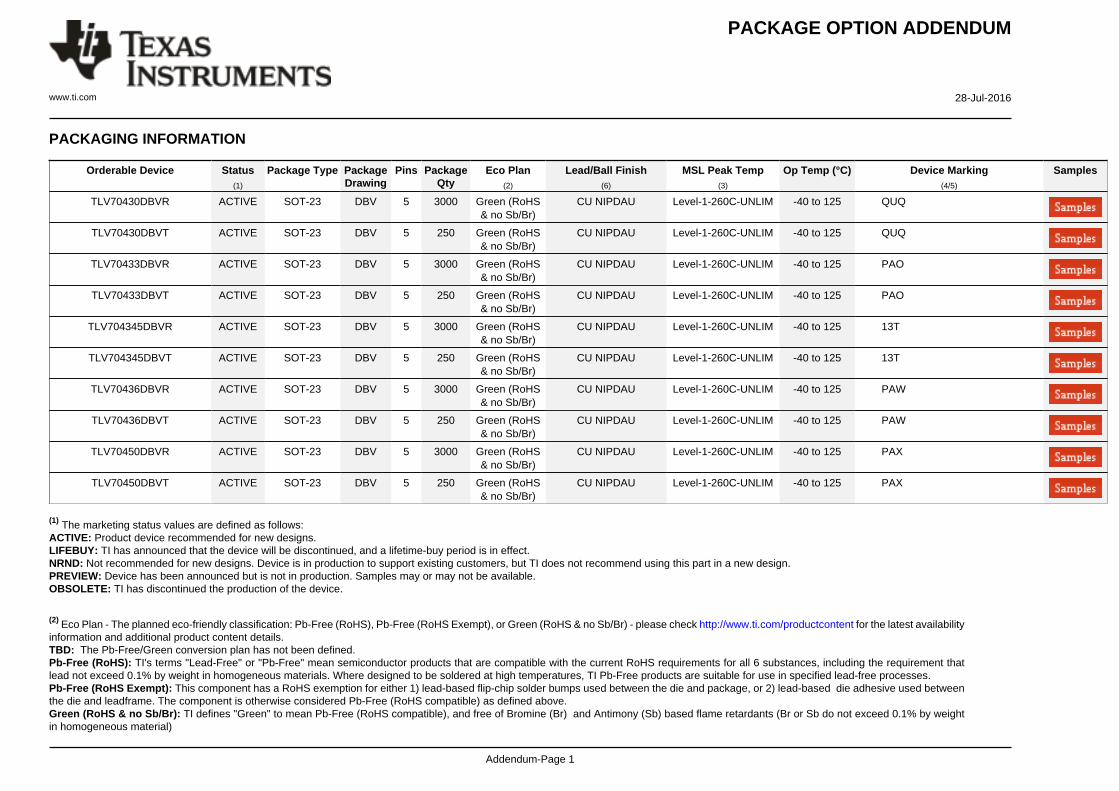
PACKAGE OPTION ADDENDUM
www.ti.com 28-Jul-2016
Addendum-Page 1
PACKAGING INFORMATION
Orderable Device Status(1)
Package Type PackageDrawing
Pins PackageQty
Eco Plan(2)
Lead/Ball Finish(6)
MSL Peak Temp(3)
Op Temp (°C) Device Marking(4/5)
Samples
TLV70430DBVR ACTIVE SOT-23 DBV 5 3000 Green (RoHS& no Sb/Br)
CU NIPDAU Level-1-260C-UNLIM -40 to 125 QUQ
TLV70430DBVT ACTIVE SOT-23 DBV 5 250 Green (RoHS& no Sb/Br)
CU NIPDAU Level-1-260C-UNLIM -40 to 125 QUQ
TLV70433DBVR ACTIVE SOT-23 DBV 5 3000 Green (RoHS& no Sb/Br)
CU NIPDAU Level-1-260C-UNLIM -40 to 125 PAO
TLV70433DBVT ACTIVE SOT-23 DBV 5 250 Green (RoHS& no Sb/Br)
CU NIPDAU Level-1-260C-UNLIM -40 to 125 PAO
TLV704345DBVR ACTIVE SOT-23 DBV 5 3000 Green (RoHS& no Sb/Br)
CU NIPDAU Level-1-260C-UNLIM -40 to 125 13T
TLV704345DBVT ACTIVE SOT-23 DBV 5 250 Green (RoHS& no Sb/Br)
CU NIPDAU Level-1-260C-UNLIM -40 to 125 13T
TLV70436DBVR ACTIVE SOT-23 DBV 5 3000 Green (RoHS& no Sb/Br)
CU NIPDAU Level-1-260C-UNLIM -40 to 125 PAW
TLV70436DBVT ACTIVE SOT-23 DBV 5 250 Green (RoHS& no Sb/Br)
CU NIPDAU Level-1-260C-UNLIM -40 to 125 PAW
TLV70450DBVR ACTIVE SOT-23 DBV 5 3000 Green (RoHS& no Sb/Br)
CU NIPDAU Level-1-260C-UNLIM -40 to 125 PAX
TLV70450DBVT ACTIVE SOT-23 DBV 5 250 Green (RoHS& no Sb/Br)
CU NIPDAU Level-1-260C-UNLIM -40 to 125 PAX
(1) The marketing status values are defined as follows:ACTIVE: Product device recommended for new designs.LIFEBUY: TI has announced that the device will be discontinued, and a lifetime-buy period is in effect.NRND: Not recommended for new designs. Device is in production to support existing customers, but TI does not recommend using this part in a new design.PREVIEW: Device has been announced but is not in production. Samples may or may not be available.OBSOLETE: TI has discontinued the production of the device.
(2) Eco Plan - The planned eco-friendly classification: Pb-Free (RoHS), Pb-Free (RoHS Exempt), or Green (RoHS & no Sb/Br) - please check http://www.ti.com/productcontent for the latest availabilityinformation and additional product content details.TBD: The Pb-Free/Green conversion plan has not been defined.Pb-Free (RoHS): TI's terms "Lead-Free" or "Pb-Free" mean semiconductor products that are compatible with the current RoHS requirements for all 6 substances, including the requirement thatlead not exceed 0.1% by weight in homogeneous materials. Where designed to be soldered at high temperatures, TI Pb-Free products are suitable for use in specified lead-free processes.Pb-Free (RoHS Exempt): This component has a RoHS exemption for either 1) lead-based flip-chip solder bumps used between the die and package, or 2) lead-based die adhesive used betweenthe die and leadframe. The component is otherwise considered Pb-Free (RoHS compatible) as defined above.Green (RoHS & no Sb/Br): TI defines "Green" to mean Pb-Free (RoHS compatible), and free of Bromine (Br) and Antimony (Sb) based flame retardants (Br or Sb do not exceed 0.1% by weightin homogeneous material)

PACKAGE OPTION ADDENDUM
www.ti.com 28-Jul-2016
Addendum-Page 2
(3) MSL, Peak Temp. - The Moisture Sensitivity Level rating according to the JEDEC industry standard classifications, and peak solder temperature.
(4) There may be additional marking, which relates to the logo, the lot trace code information, or the environmental category on the device.
(5) Multiple Device Markings will be inside parentheses. Only one Device Marking contained in parentheses and separated by a "~" will appear on a device. If a line is indented then it is a continuationof the previous line and the two combined represent the entire Device Marking for that device.
(6) Lead/Ball Finish - Orderable Devices may have multiple material finish options. Finish options are separated by a vertical ruled line. Lead/Ball Finish values may wrap to two lines if the finishvalue exceeds the maximum column width.
Important Information and Disclaimer:The information provided on this page represents TI's knowledge and belief as of the date that it is provided. TI bases its knowledge and belief on informationprovided by third parties, and makes no representation or warranty as to the accuracy of such information. Efforts are underway to better integrate information from third parties. TI has taken andcontinues to take reasonable steps to provide representative and accurate information but may not have conducted destructive testing or chemical analysis on incoming materials and chemicals.TI and TI suppliers consider certain information to be proprietary, and thus CAS numbers and other limited information may not be available for release.
In no event shall TI's liability arising out of such information exceed the total purchase price of the TI part(s) at issue in this document sold by TI to Customer on an annual basis.
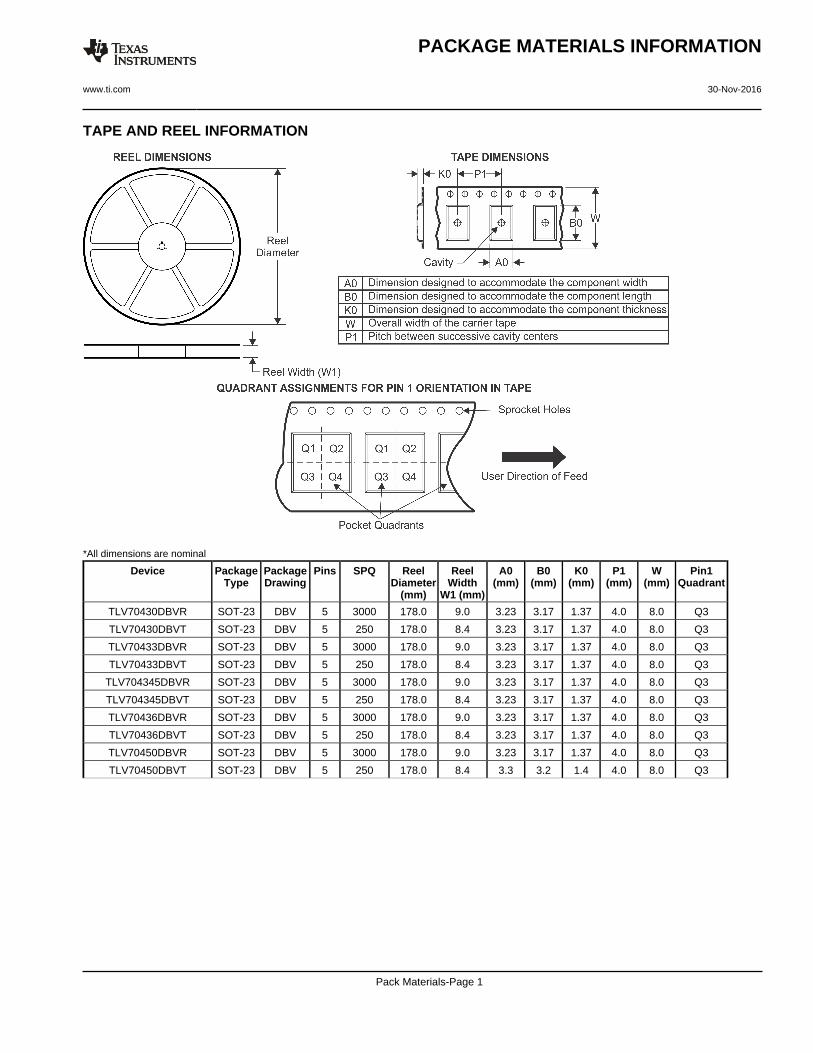
TAPE AND REEL INFORMATION
*All dimensions are nominal
Device PackageType
PackageDrawing
Pins SPQ ReelDiameter
(mm)
ReelWidth
W1 (mm)
A0(mm)
B0(mm)
K0(mm)
P1(mm)
W(mm)
Pin1Quadrant
TLV70430DBVR SOT-23 DBV 5 3000 178.0 9.0 3.23 3.17 1.37 4.0 8.0 Q3
TLV70430DBVT SOT-23 DBV 5 250 178.0 8.4 3.23 3.17 1.37 4.0 8.0 Q3
TLV70433DBVR SOT-23 DBV 5 3000 178.0 9.0 3.23 3.17 1.37 4.0 8.0 Q3
TLV70433DBVT SOT-23 DBV 5 250 178.0 8.4 3.23 3.17 1.37 4.0 8.0 Q3
TLV704345DBVR SOT-23 DBV 5 3000 178.0 9.0 3.23 3.17 1.37 4.0 8.0 Q3
TLV704345DBVT SOT-23 DBV 5 250 178.0 8.4 3.23 3.17 1.37 4.0 8.0 Q3
TLV70436DBVR SOT-23 DBV 5 3000 178.0 9.0 3.23 3.17 1.37 4.0 8.0 Q3
TLV70436DBVT SOT-23 DBV 5 250 178.0 8.4 3.23 3.17 1.37 4.0 8.0 Q3
TLV70450DBVR SOT-23 DBV 5 3000 178.0 9.0 3.23 3.17 1.37 4.0 8.0 Q3
TLV70450DBVT SOT-23 DBV 5 250 178.0 8.4 3.3 3.2 1.4 4.0 8.0 Q3
PACKAGE MATERIALS INFORMATION
www.ti.com 30-Nov-2016
Pack Materials-Page 1
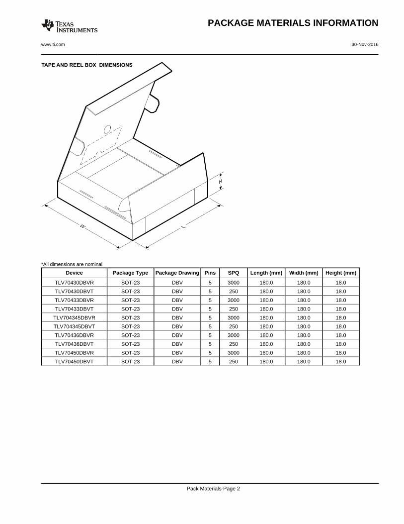
*All dimensions are nominal
Device Package Type Package Drawing Pins SPQ Length (mm) Width (mm) Height (mm)
TLV70430DBVR SOT-23 DBV 5 3000 180.0 180.0 18.0
TLV70430DBVT SOT-23 DBV 5 250 180.0 180.0 18.0
TLV70433DBVR SOT-23 DBV 5 3000 180.0 180.0 18.0
TLV70433DBVT SOT-23 DBV 5 250 180.0 180.0 18.0
TLV704345DBVR SOT-23 DBV 5 3000 180.0 180.0 18.0
TLV704345DBVT SOT-23 DBV 5 250 180.0 180.0 18.0
TLV70436DBVR SOT-23 DBV 5 3000 180.0 180.0 18.0
TLV70436DBVT SOT-23 DBV 5 250 180.0 180.0 18.0
TLV70450DBVR SOT-23 DBV 5 3000 180.0 180.0 18.0
TLV70450DBVT SOT-23 DBV 5 250 180.0 180.0 18.0
PACKAGE MATERIALS INFORMATION
www.ti.com 30-Nov-2016
Pack Materials-Page 2


www.ti.com
PACKAGE OUTLINE
C
TYP0.220.08
0.25
3.02.6
2X 0.95
1.9
1.45 MAX
TYP0.150.00
5X 0.50.3
TYP0.60.3
TYP80
1.9
A
3.052.75
B1.751.45
(1.1)
SOT-23 - 1.45 mm max heightDBV0005ASMALL OUTLINE TRANSISTOR
4214839/C 04/2017
NOTES: 1. All linear dimensions are in millimeters. Any dimensions in parenthesis are for reference only. Dimensioning and tolerancing per ASME Y14.5M.2. This drawing is subject to change without notice.3. Refernce JEDEC MO-178.
0.2 C A B
1
34
5
2
INDEX AREAPIN 1
GAGE PLANE
SEATING PLANE
0.1 C
SCALE 4.000

www.ti.com
EXAMPLE BOARD LAYOUT
0.07 MAXARROUND
0.07 MINARROUND
5X (1.1)
5X (0.6)
(2.6)
(1.9)
2X (0.95)
(R0.05) TYP
4214839/C 04/2017
SOT-23 - 1.45 mm max heightDBV0005ASMALL OUTLINE TRANSISTOR
NOTES: (continued) 4. Publication IPC-7351 may have alternate designs. 5. Solder mask tolerances between and around signal pads can vary based on board fabrication site.
SYMM
LAND PATTERN EXAMPLEEXPOSED METAL SHOWN
SCALE:15X
PKG
1
3 4
5
2
SOLDER MASKOPENINGMETAL UNDER
SOLDER MASK
SOLDER MASKDEFINED
EXPOSED METAL
METALSOLDER MASKOPENING
NON SOLDER MASKDEFINED
(PREFERRED)
SOLDER MASK DETAILS
EXPOSED METAL

www.ti.com
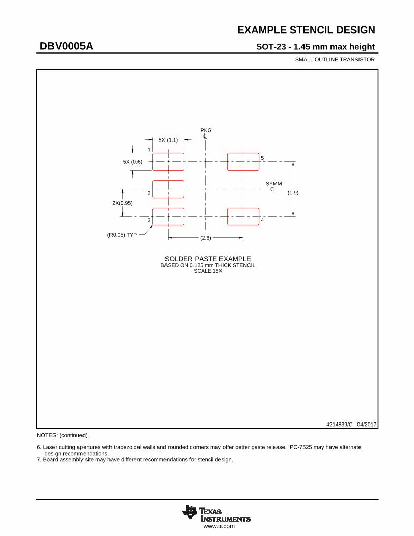
EXAMPLE STENCIL DESIGN
(2.6)
(1.9)
2X(0.95)
5X (1.1)
5X (0.6)
(R0.05) TYP
SOT-23 - 1.45 mm max heightDBV0005ASMALL OUTLINE TRANSISTOR
4214839/C 04/2017
NOTES: (continued) 6. Laser cutting apertures with trapezoidal walls and rounded corners may offer better paste release. IPC-7525 may have alternate design recommendations. 7. Board assembly site may have different recommendations for stencil design.
SOLDER PASTE EXAMPLEBASED ON 0.125 mm THICK STENCIL
SCALE:15X
SYMM
PKG
1
3 4
5
2

www.ti.com
PACKAGE OUTLINE
C
TYP0.220.08
0.25
3.02.6
2X 0.95
1.9
1.45 MAX
TYP0.150.00
5X 0.50.3
TYP0.60.3
TYP80
1.9
A
3.052.75
B1.751.45
(1.1)
SOT-23 - 1.45 mm max heightDBV0005ASMALL OUTLINE TRANSISTOR
4214839/C 04/2017
NOTES: 1. All linear dimensions are in millimeters. Any dimensions in parenthesis are for reference only. Dimensioning and tolerancing per ASME Y14.5M.2. This drawing is subject to change without notice.3. Refernce JEDEC MO-178.
0.2 C A B
1
34
5
2
INDEX AREAPIN 1
GAGE PLANE
SEATING PLANE
0.1 C
SCALE 4.000

www.ti.com
EXAMPLE BOARD LAYOUT
0.07 MAXARROUND
0.07 MINARROUND
5X (1.1)
5X (0.6)
(2.6)
(1.9)
2X (0.95)
(R0.05) TYP
4214839/C 04/2017
SOT-23 - 1.45 mm max heightDBV0005ASMALL OUTLINE TRANSISTOR
NOTES: (continued) 4. Publication IPC-7351 may have alternate designs. 5. Solder mask tolerances between and around signal pads can vary based on board fabrication site.
SYMM
LAND PATTERN EXAMPLEEXPOSED METAL SHOWN
SCALE:15X
PKG
1
3 4
5
2
SOLDER MASKOPENINGMETAL UNDER
SOLDER MASK
SOLDER MASKDEFINED
EXPOSED METAL
METALSOLDER MASKOPENING
NON SOLDER MASKDEFINED
(PREFERRED)
SOLDER MASK DETAILS
EXPOSED METAL
www.ti.com
EXAMPLE STENCIL DESIGN
(2.6)
(1.9)
2X(0.95)
5X (1.1)
5X (0.6)
(R0.05) TYP
SOT-23 - 1.45 mm max heightDBV0005ASMALL OUTLINE TRANSISTOR
4214839/C 04/2017
NOTES: (continued) 6. Laser cutting apertures with trapezoidal walls and rounded corners may offer better paste release. IPC-7525 may have alternate design recommendations. 7. Board assembly site may have different recommendations for stencil design.
SOLDER PASTE EXAMPLEBASED ON 0.125 mm THICK STENCIL
SCALE:15X
SYMM
PKG
1
3 4
5
2

IMPORTANT NOTICE
Texas Instruments Incorporated (TI) reserves the right to make corrections, enhancements, improvements and other changes to itssemiconductor products and services per JESD46, latest issue, and to discontinue any product or service per JESD48, latest issue. Buyersshould obtain the latest relevant information before placing orders and should verify that such information is current and complete.TI’s published terms of sale for semiconductor products (http://www.ti.com/sc/docs/stdterms.htm) apply to the sale of packaged integratedcircuit products that TI has qualified and released to market. Additional terms may apply to the use or sale of other types of TI products andservices.Reproduction of significant portions of TI information in TI data sheets is permissible only if reproduction is without alteration and isaccompanied by all associated warranties, conditions, limitations, and notices. TI is not responsible or liable for such reproduceddocumentation. Information of third parties may be subject to additional restrictions. Resale of TI products or services with statementsdifferent from or beyond the parameters stated by TI for that product or service voids all express and any implied warranties for theassociated TI product or service and is an unfair and deceptive business practice. TI is not responsible or liable for any such statements.Buyers and others who are developing systems that incorporate TI products (collectively, “Designers”) understand and agree that Designersremain responsible for using their independent analysis, evaluation and judgment in designing their applications and that Designers havefull and exclusive responsibility to assure the safety of Designers' applications and compliance of their applications (and of all TI productsused in or for Designers’ applications) with all applicable regulations, laws and other applicable requirements. Designer represents that, withrespect to their applications, Designer has all the necessary expertise to create and implement safeguards that (1) anticipate dangerousconsequences of failures, (2) monitor failures and their consequences, and (3) lessen the likelihood of failures that might cause harm andtake appropriate actions. Designer agrees that prior to using or distributing any applications that include TI products, Designer willthoroughly test such applications and the functionality of such TI products as used in such applications.TI’s provision of technical, application or other design advice, quality characterization, reliability data or other services or information,including, but not limited to, reference designs and materials relating to evaluation modules, (collectively, “TI Resources”) are intended toassist designers who are developing applications that incorporate TI products; by downloading, accessing or using TI Resources in anyway, Designer (individually or, if Designer is acting on behalf of a company, Designer’s company) agrees to use any particular TI Resourcesolely for this purpose and subject to the terms of this Notice.TI’s provision of TI Resources does not expand or otherwise alter TI’s applicable published warranties or warranty disclaimers for TIproducts, and no additional obligations or liabilities arise from TI providing such TI Resources. TI reserves the right to make corrections,enhancements, improvements and other changes to its TI Resources. TI has not conducted any testing other than that specificallydescribed in the published documentation for a particular TI Resource.Designer is authorized to use, copy and modify any individual TI Resource only in connection with the development of applications thatinclude the TI product(s) identified in such TI Resource. NO OTHER LICENSE, EXPRESS OR IMPLIED, BY ESTOPPEL OR OTHERWISETO ANY OTHER TI INTELLECTUAL PROPERTY RIGHT, AND NO LICENSE TO ANY TECHNOLOGY OR INTELLECTUAL PROPERTYRIGHT OF TI OR ANY THIRD PARTY IS GRANTED HEREIN, including but not limited to any patent right, copyright, mask work right, orother intellectual property right relating to any combination, machine, or process in which TI products or services are used. Informationregarding or referencing third-party products or services does not constitute a license to use such products or services, or a warranty orendorsement thereof. Use of TI Resources may require a license from a third party under the patents or other intellectual property of thethird party, or a license from TI under the patents or other intellectual property of TI.TI RESOURCES ARE PROVIDED “AS IS” AND WITH ALL FAULTS. TI DISCLAIMS ALL OTHER WARRANTIES ORREPRESENTATIONS, EXPRESS OR IMPLIED, REGARDING RESOURCES OR USE THEREOF, INCLUDING BUT NOT LIMITED TOACCURACY OR COMPLETENESS, TITLE, ANY EPIDEMIC FAILURE WARRANTY AND ANY IMPLIED WARRANTIES OFMERCHANTABILITY, FITNESS FOR A PARTICULAR PURPOSE, AND NON-INFRINGEMENT OF ANY THIRD PARTY INTELLECTUALPROPERTY RIGHTS. TI SHALL NOT BE LIABLE FOR AND SHALL NOT DEFEND OR INDEMNIFY DESIGNER AGAINST ANY CLAIM,INCLUDING BUT NOT LIMITED TO ANY INFRINGEMENT CLAIM THAT RELATES TO OR IS BASED ON ANY COMBINATION OFPRODUCTS EVEN IF DESCRIBED IN TI RESOURCES OR OTHERWISE. IN NO EVENT SHALL TI BE LIABLE FOR ANY ACTUAL,DIRECT, SPECIAL, COLLATERAL, INDIRECT, PUNITIVE, INCIDENTAL, CONSEQUENTIAL OR EXEMPLARY DAMAGES INCONNECTION WITH OR ARISING OUT OF TI RESOURCES OR USE THEREOF, AND REGARDLESS OF WHETHER TI HAS BEENADVISED OF THE POSSIBILITY OF SUCH DAMAGES.Unless TI has explicitly designated an individual product as meeting the requirements of a particular industry standard (e.g., ISO/TS 16949and ISO 26262), TI is not responsible for any failure to meet such industry standard requirements.Where TI specifically promotes products as facilitating functional safety or as compliant with industry functional safety standards, suchproducts are intended to help enable customers to design and create their own applications that meet applicable functional safety standardsand requirements. Using products in an application does not by itself establish any safety features in the application. Designers mustensure compliance with safety-related requirements and standards applicable to their applications. Designer may not use any TI products inlife-critical medical equipment unless authorized officers of the parties have executed a special contract specifically governing such use.Life-critical medical equipment is medical equipment where failure of such equipment would cause serious bodily injury or death (e.g., lifesupport, pacemakers, defibrillators, heart pumps, neurostimulators, and implantables). Such equipment includes, without limitation, allmedical devices identified by the U.S. Food and Drug Administration as Class III devices and equivalent classifications outside the U.S.TI may expressly designate certain products as completing a particular qualification (e.g., Q100, Military Grade, or Enhanced Product).Designers agree that it has the necessary expertise to select the product with the appropriate qualification designation for their applicationsand that proper product selection is at Designers’ own risk. Designers are solely responsible for compliance with all legal and regulatoryrequirements in connection with such selection.Designer will fully indemnify TI and its representatives against any damages, costs, losses, and/or liabilities arising out of Designer’s non-compliance with the terms and provisions of this Notice.
Mailing Address: Texas Instruments, Post Office Box 655303, Dallas, Texas 75265Copyright © 2018, Texas Instruments Incorporated