1 features 2 applications 3 description - ti.com
TRANSCRIPT

TPS92662-Q1 High-brightness LED Matrix Manager for Automotive Headlight Systems
1 Features• AEC-Q100 qualified for automotive applications
– Grade 1: –40°C to 125°C ambient operatingtemperature
– Device HBM classification level H1C– Device CDM classification level C5
• Input voltage range: 4.5 V to 60 V• 12 Integrated bypass switches
– Four sub-strings of three series switches– 20-V maximum across switch– 62-V maximum switch to ground
• Multi-drop UART communication interface– Up to 31 addressable devices
• Compatible with CAN physical layer– Minimum number of wires in cable harness
• Eight-bit ADC with two MUXed inputs• Crystal oscillator driver• External EEPROM I2C interface• Programmable 10-bit PWM dimming
– Individual phase shift and pulse width– Device-to-device synchronization
• LED open and short detection and protection
2 Applications• Automotive headlight systems• High-brightness LED matrix systems• ADB or glare-free high beam• Sequential turn and animated daytime running
lights
3 DescriptionThe TPS92662-Q1 LED matrix manager deviceenables fully dynamic adaptive lighting solutions byproviding individual pixel-level LED control.
The device includes four sub-strings of three series-connected integrated switches for bypassingindividual LEDs. The individual sub-strings allow thedevice to accept either single or multiple currentsources. It also allows paralleling up to four switchesfor bypassing high current LEDs.
A master microcontroller is used to control andmanage the TPS92662-Q1 devices via a multi-dropuniversal asynchronous receiver transmitter (UART)serial interface. The serial interface supports the useof CAN transceivers for a more robust physical layer.The I2C communication interface can be used to readfrom and write to an external EEPROM that can storesystem calibration data.
An on-board 8-bit ADC with two multiplexed inputscan be used for system temperature compensationand used to measure a binning value which allows forLED binning and coding.
The internal charge pump rail supplies the gate drivevoltage for the LED bypass switches. The low on-resistance (RDS(on)) of the bypass switch minimizesconduction loss and power dissipation.
The phase shift and pulse width for each individualLED in the string are programmable. The device usesan internal register to adjust the PWM frequency.Multiple devices can be synchronized. The switchtransitions during PWM dimming operation have aprogrammable slew rate to mitigate EMI concerns.
The device features open LED protection withprogrammable threshold. The serial interface reportsopen LED or short LED faults.
Device InformationPART NUMBER PACKAGE(1) BODY SIZE (NOM)
TPS92662-Q1 PHP (48) 7.00 mm × 7.00 mm
(1) For all available packages, see the orderable addendum atthe end of the data sheet.
CAN
VDD VIO GND
TX
RX
SDA
SCL
E2
UART
I2C
LEDx
VIN
XTALI
XTALO
CAN
MCU
BUCKBOOST
ECU
VBAT
TPS92662
BIN ADCx
CPPx
Simplified Application
www.ti.comTPS92662-Q1
SLUSD15B – OCTOBER 2018 – REVISED JUNE 2020
Copyright © 2020 Texas Instruments Incorporated Submit Document Feedback 1
Product Folder Links: TPS92662-Q1
TPS92662-Q1SLUSD15B – OCTOBER 2018 – REVISED JUNE 2020
An IMPORTANT NOTICE at the end of this data sheet addresses availability, warranty, changes, use in safety-critical applications,intellectual property matters and other important disclaimers. PRODUCTION DATA.

Table of Contents1 Features............................................................................12 Applications..................................................................... 13 Description.......................................................................14 Revision History.............................................................. 25 Device and Documentation Support..............................3
5.1 Receiving Notification of Documentation Updates......3
5.2 Support Resources..................................................... 35.3 Trademarks.................................................................35.4 Electrostatic Discharge Caution..................................35.5 Glossary......................................................................3
6 Mechanical, Packaging, and Orderable Information.... 4
4 Revision HistoryNOTE: Page numbers for previous revisions may differ from page numbers in the current version.
Changes from Revision A (January 2019) to Revision B (July 2020) Page• Added the CLK low-level (VIH-TH) and high-level (VIH-TH threshold input voltage thresholds to the Electrical
Characteristics ................................................................................................................................................... 1• Updated the numbering format for tables, figures and cross-references throughout the document...................1
Changes from Revision * (June 2017) to Revision A (January 2019) Page• Updated Section 2 ............................................................................................................................................. 1• Updated Section 3 ............................................................................................................................................. 1
TPS92662-Q1SLUSD15B – OCTOBER 2018 – REVISED JUNE 2020 www.ti.com
2 Submit Document Feedback Copyright © 2020 Texas Instruments Incorporated
Product Folder Links: TPS92662-Q1

5 Device and Documentation Support5.1 Receiving Notification of Documentation UpdatesTo receive notification of documentation updates, navigate to the device product folder on ti.com. Click onSubscribe to updates to register and receive a weekly digest of any product information that has changed. Forchange details, review the revision history included in any revised document.
5.2 Support ResourcesTI E2E™ support forums are an engineer's go-to source for fast, verified answers and design help — straightfrom the experts. Search existing answers or ask your own question to get the quick design help you need.
Linked content is provided "AS IS" by the respective contributors. They do not constitute TI specifications and donot necessarily reflect TI's views; see TI's Terms of Use.
5.3 TrademarksTI E2E™ is a trademark of Texas Instruments Incorporated.All other trademarks are the property of their respective owners.5.4 Electrostatic Discharge Caution
This integrated circuit can be damaged by ESD. Texas Instruments recommends that all integrated circuits be handledwith appropriate precautions. Failure to observe proper handling and installation procedures can cause damage.ESD damage can range from subtle performance degradation to complete device failure. Precision integrated circuits maybe more susceptible to damage because very small parametric changes could cause the device not to meet its publishedspecifications.
5.5 GlossaryTI Glossary This glossary lists and explains terms, acronyms, and definitions.
www.ti.comTPS92662-Q1
SLUSD15B – OCTOBER 2018 – REVISED JUNE 2020
Copyright © 2020 Texas Instruments Incorporated Submit Document Feedback 3
Product Folder Links: TPS92662-Q1

6 Mechanical, Packaging, and Orderable InformationThe following pages include mechanical, packaging, and orderable information. This information is the mostcurrent data available for the designated devices. This data is subject to change without notice and revision ofthis document. For browser-based versions of this data sheet, refer to the left-hand navigation.
TPS92662-Q1SLUSD15B – OCTOBER 2018 – REVISED JUNE 2020 www.ti.com
4 Submit Document Feedback Copyright © 2020 Texas Instruments Incorporated
Product Folder Links: TPS92662-Q1

PACKAGE OPTION ADDENDUM
www.ti.com 10-Dec-2020
Addendum-Page 1
PACKAGING INFORMATION
Orderable Device Status(1)
Package Type PackageDrawing
Pins PackageQty
Eco Plan(2)
Lead finish/Ball material
(6)
MSL Peak Temp(3)
Op Temp (°C) Device Marking(4/5)
Samples
TPS92662QPHPRQ1 ACTIVE HTQFP PHP 48 1000 RoHS & Green NIPDAU Level-3-260C-168 HR -40 to 125 92662Q
TPS92662QPHPTQ1 ACTIVE HTQFP PHP 48 250 RoHS & Green NIPDAU Level-3-260C-168 HR -40 to 125 92662Q
(1) The marketing status values are defined as follows:ACTIVE: Product device recommended for new designs.LIFEBUY: TI has announced that the device will be discontinued, and a lifetime-buy period is in effect.NRND: Not recommended for new designs. Device is in production to support existing customers, but TI does not recommend using this part in a new design.PREVIEW: Device has been announced but is not in production. Samples may or may not be available.OBSOLETE: TI has discontinued the production of the device.
(2) RoHS: TI defines "RoHS" to mean semiconductor products that are compliant with the current EU RoHS requirements for all 10 RoHS substances, including the requirement that RoHS substancedo not exceed 0.1% by weight in homogeneous materials. Where designed to be soldered at high temperatures, "RoHS" products are suitable for use in specified lead-free processes. TI mayreference these types of products as "Pb-Free".RoHS Exempt: TI defines "RoHS Exempt" to mean products that contain lead but are compliant with EU RoHS pursuant to a specific EU RoHS exemption.Green: TI defines "Green" to mean the content of Chlorine (Cl) and Bromine (Br) based flame retardants meet JS709B low halogen requirements of <=1000ppm threshold. Antimony trioxide basedflame retardants must also meet the <=1000ppm threshold requirement.
(3) MSL, Peak Temp. - The Moisture Sensitivity Level rating according to the JEDEC industry standard classifications, and peak solder temperature.
(4) There may be additional marking, which relates to the logo, the lot trace code information, or the environmental category on the device.
(5) Multiple Device Markings will be inside parentheses. Only one Device Marking contained in parentheses and separated by a "~" will appear on a device. If a line is indented then it is a continuationof the previous line and the two combined represent the entire Device Marking for that device.
(6) Lead finish/Ball material - Orderable Devices may have multiple material finish options. Finish options are separated by a vertical ruled line. Lead finish/Ball material values may wrap to twolines if the finish value exceeds the maximum column width.
Important Information and Disclaimer:The information provided on this page represents TI's knowledge and belief as of the date that it is provided. TI bases its knowledge and belief on informationprovided by third parties, and makes no representation or warranty as to the accuracy of such information. Efforts are underway to better integrate information from third parties. TI has taken andcontinues to take reasonable steps to provide representative and accurate information but may not have conducted destructive testing or chemical analysis on incoming materials and chemicals.TI and TI suppliers consider certain information to be proprietary, and thus CAS numbers and other limited information may not be available for release.
In no event shall TI's liability arising out of such information exceed the total purchase price of the TI part(s) at issue in this document sold by TI to Customer on an annual basis.

PACKAGE OPTION ADDENDUM
www.ti.com 10-Dec-2020
Addendum-Page 2

TAPE AND REEL INFORMATION
*All dimensions are nominal
Device PackageType
PackageDrawing
Pins SPQ ReelDiameter
(mm)
ReelWidth
W1 (mm)
A0(mm)
B0(mm)
K0(mm)
P1(mm)
W(mm)
Pin1Quadrant
TPS92662QPHPRQ1 HTQFP PHP 48 1000 330.0 16.4 9.6 9.6 1.5 12.0 16.0 Q2
TPS92662QPHPTQ1 HTQFP PHP 48 250 330.0 16.4 9.6 9.6 1.5 12.0 16.0 Q2
PACKAGE MATERIALS INFORMATION
www.ti.com 1-Sep-2021
Pack Materials-Page 1

*All dimensions are nominal
Device Package Type Package Drawing Pins SPQ Length (mm) Width (mm) Height (mm)
TPS92662QPHPRQ1 HTQFP PHP 48 1000 336.6 336.6 31.8
TPS92662QPHPTQ1 HTQFP PHP 48 250 336.6 336.6 31.8
PACKAGE MATERIALS INFORMATION
www.ti.com 1-Sep-2021
Pack Materials-Page 2

www.ti.com
GENERIC PACKAGE VIEW
This image is a representation of the package family, actual package may vary.Refer to the product data sheet for package details.
TQFP - 1.2 mm max heightPHP 48QUAD FLATPACK7 x 7, 0.5 mm pitch
4226443/A
www.ti.com
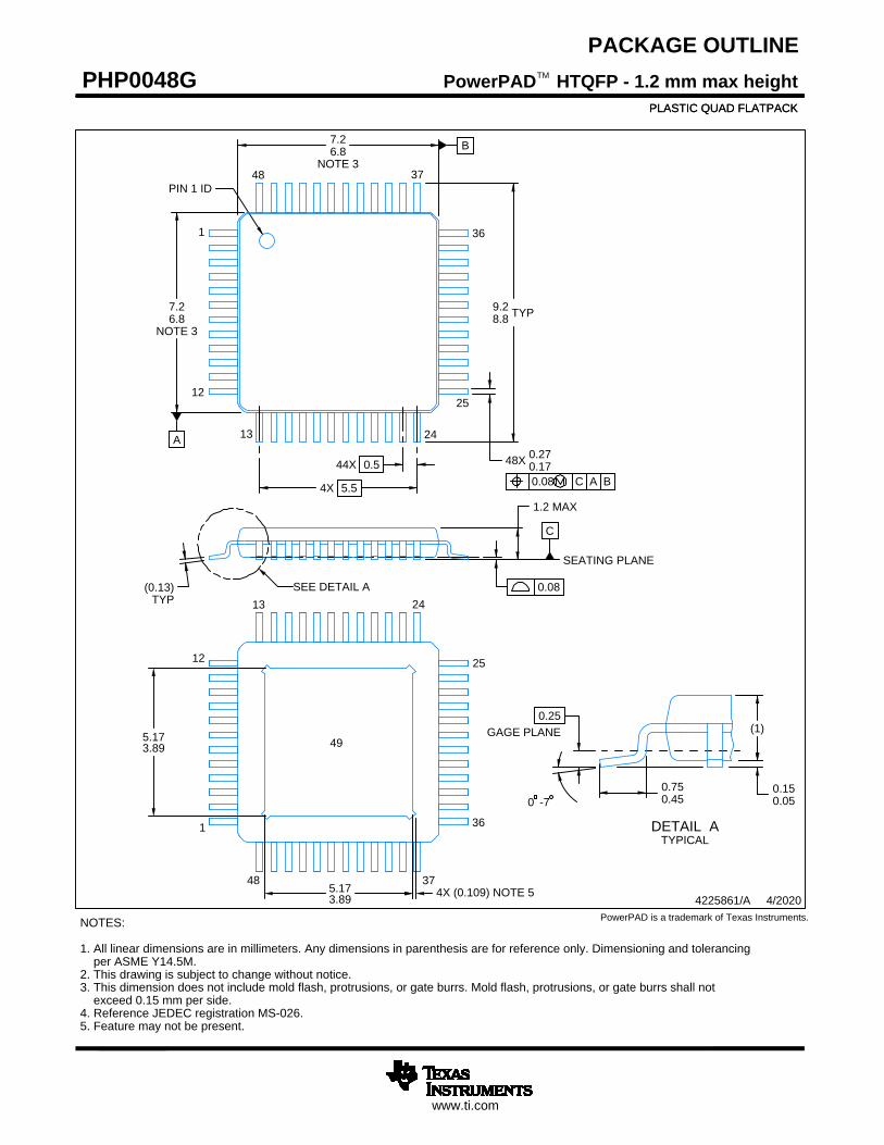
PACKAGE OUTLINE
C
48X
0.27
0.17
44X 0.5
PIN 1 ID
(0.13)
TYP
0.15
0.05
0 -7
4X 5.5
9.2
8.8
TYP
0.75
0.45
B
7.2
6.8
NOTE 3
A
7.2
6.8
NOTE 3
0.25
GAGE PLANE
1.2 MAX
(1)
PowerPAD HTQFP - 1.2 mm max heightPHP0048G
PLASTIC QUAD FLATPACK
NOTES:
1. All linear dimensions are in millimeters. Any dimensions in parenthesis are for reference only. Dimensioning and tolerancing
per ASME Y14.5M.
2. This drawing is subject to change without notice.
3. This dimension does not include mold flash, protrusions, or gate burrs. Mold flash, protrusions, or gate burrs shall not
exceed 0.15 mm per side.
4. Reference JEDEC registration MS-026.
5. Feature may not be present.
TM
PowerPAD is a trademark of Texas Instruments.
1
12
1324
25
36
3748
0.08 C A B
SEE DETAIL A
SEATING PLANE
0.08
A 16
DETAIL A
TYPICAL
SCALE 1.900
1
12
13 24
25
36
3748
49
PLASTIC QUAD FLATPACK
4225861/A 4/2020
5.17
3.89
5.17
3.89
4X (0.109) NOTE 5

www.ti.com
EXAMPLE BOARD LAYOUT
0.05 MAX
ALL AROUND
0.05 MIN
ALL AROUND
(8.5)
(8.5)
44X (0.5)
48X (1.6)
48X (0.3)
( 0.2) TYP
VIA
( 6.5)
NOTE 10
(R0.05) TYP
(1.1 TYP)
(1.1 TYP)
PowerPAD HTQFP - 1.2 mm max heightPHP0048G
PLASTIC QUAD FLATPACK
NOTES: (continued)
6. Publication IPC-7351 may have alternate designs.
7. Solder mask tolerances between and around signal pads can vary based on board fabrication site.
8. This package is designed to be soldered to a thermal pad on the board. See technical brief, Powerpad thermally enhanced package,
Texas Instruments Literature No. SLMA002 (www.ti.com/lit/slma002) and SLMA004 (www.ti.com/lit/slma004).
9. Vias are optional depending on application, refer to device data sheet. It is recommended that vias under paste be filled, plugged
or tented.
10. Size of metal pad may vary due to creepage requirement.
TM
LAND PATTERN EXAMPLE
EXPOSED METAL SHOWN
SCALE:8X
SYMM
SYMM
48 37
13 24
25
36
1
12
SOLDER MASK
DEFINED PAD
METAL COVERED
BY SOLDER MASK
49
SEE DETAILS
METAL
SOLDER MASK
OPENING
NON SOLDER MASK
DEFINED
SOLDER MASK DETAILS
EXPOSED METAL
SOLDER MASK
OPENING
METAL UNDER
SOLDER MASK
SOLDER MASK
DEFINED
EXPOSED METAL
4225861/A 4/2020
(5.17)
(5.17)

www.ti.com
EXAMPLE STENCIL DESIGN
44X (0.5)
48X (1.6)
48X (0.3)
(R0.05) TYP
(8.5)
(8.5)
PowerPAD HTQFP - 1.2 mm max heightPHP0048G
PLASTIC QUAD FLATPACK
NOTES: (continued)
11. Laser cutting apertures with trapezoidal walls and rounded corners may offer better paste release. IPC-7525 may have alternate
design recommendations.
12. Board assembly site may have different recommendations for stencil design.
TM
SOLDER PASTE EXAMPLE
EXPOSED PAD
100% PRINTED SOLDER COVERAGE BY AREA
SCALE:8X
SEE TABLE FOR
DIFFERENT OPENINGS
FOR OTHER STENCIL
THICKNESSES
BASED ON
0.125 THICK STENCIL
SYMM
SYMM
48 37
1324
25
36
1
12
METAL COVERED
BY SOLDER MASK
49
4.37 X 4.370.175
4.72 X 4.720.150
5.17 X 5.17 (SHOWN)0.125
5.78 X 5.780.1
SOLDER STENCIL
OPENING
STENCIL
THICKNESS
4225861/A 4/2020
(5.17)
(5.17)
BASED ON
0.125 THICK
STENCIL

IMPORTANT NOTICE AND DISCLAIMERTI PROVIDES TECHNICAL AND RELIABILITY DATA (INCLUDING DATASHEETS), DESIGN RESOURCES (INCLUDING REFERENCEDESIGNS), APPLICATION OR OTHER DESIGN ADVICE, WEB TOOLS, SAFETY INFORMATION, AND OTHER RESOURCES “AS IS”AND WITH ALL FAULTS, AND DISCLAIMS ALL WARRANTIES, EXPRESS AND IMPLIED, INCLUDING WITHOUT LIMITATION ANYIMPLIED WARRANTIES OF MERCHANTABILITY, FITNESS FOR A PARTICULAR PURPOSE OR NON-INFRINGEMENT OF THIRDPARTY INTELLECTUAL PROPERTY RIGHTS.These resources are intended for skilled developers designing with TI products. You are solely responsible for (1) selecting the appropriateTI products for your application, (2) designing, validating and testing your application, and (3) ensuring your application meets applicablestandards, and any other safety, security, or other requirements. These resources are subject to change without notice. TI grants youpermission to use these resources only for development of an application that uses the TI products described in the resource. Otherreproduction and display of these resources is prohibited. No license is granted to any other TI intellectual property right or to any third partyintellectual property right. TI disclaims responsibility for, and you will fully indemnify TI and its representatives against, any claims, damages,costs, losses, and liabilities arising out of your use of these resources.TI’s products are provided subject to TI’s Terms of Sale (https:www.ti.com/legal/termsofsale.html) or other applicable terms available eitheron ti.com or provided in conjunction with such TI products. TI’s provision of these resources does not expand or otherwise alter TI’sapplicable warranties or warranty disclaimers for TI products.IMPORTANT NOTICE
Mailing Address: Texas Instruments, Post Office Box 655303, Dallas, Texas 75265Copyright © 2021, Texas Instruments Incorporated