1 design of 8- bit alu neelam chaudhari archana mulukutla namita mittal madhumita sanyal advisor :...
Post on 20-Dec-2015
244 views
TRANSCRIPT
1
Design of 8- Bit ALU
Neelam Chaudhari
Archana Mulukutla
Namita Mittal
Madhumita Sanyal
Advisor : Dr. David Parent
Date : May 8, 2006
2
Agenda• Abstract• Introduction
– Why– Theory behind.– Back Ground information (Lit. Review)
• Summary of Results• Project (Experimental) Details• Results• Cost Analysis• Conclusions
3
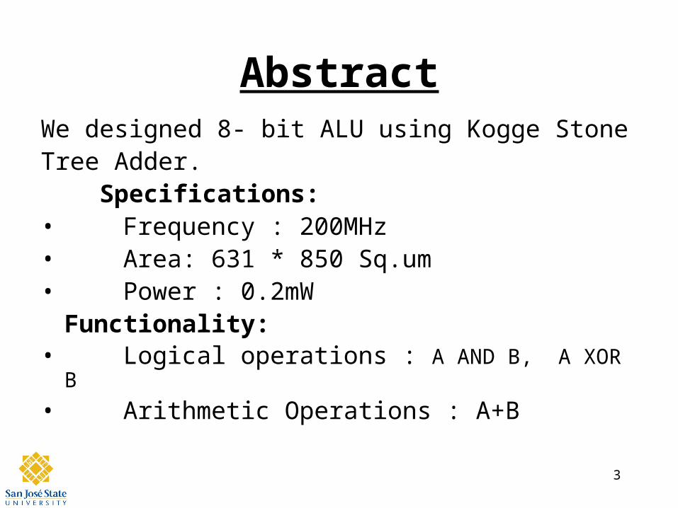
AbstractWe designed 8- bit ALU using Kogge StoneTree Adder. Specifications:• Frequency : 200MHz• Area: 631 * 850 Sq.um• Power : 0.2mW
Functionality:• Logical operations : A AND B, A XOR B
• Arithmetic Operations : A+B
4
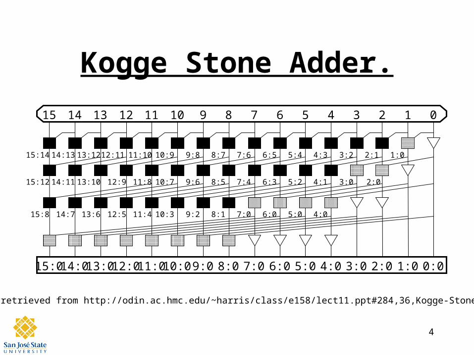
Kogge Stone Adder.
1:02:13:24:35:46:57:68:79:810:911:1012:1113:1214:1315:14
3:04:15:26:37:48:59:610:711:812:913:1014:1115:12
4:05:06:07:08:19:210:311:412:513:614:715:8
2:0
0123456789101112131415
15:0 14:0 13:0 12:0 11:0 10:0 9:0 8:0 7:0 6:0 5:0 4:0 3:0 2:0 1:0 0:0
(retrieved from http://odin.ac.hmc.edu/~harris/class/e158/lect11.ppt#284,36,Kogge-Stone)
5
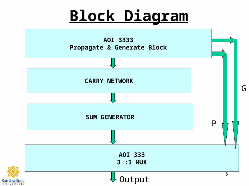
Block Diagram
AOI 3333Propagate & Generate Block
CARRY NETWORK
SUM GENERATOR
AOI 3333 :1 MUX
Output
P
G

6
IntroductionWhy this Project?
• ALU is Basic Building Block of several circuits.
• Challenging to implement CLA with least number of logic levels and fan-ins.
• Look ahead across the look-ahead carry tree.
• Gives us a hands-on design experience on the concepts learnt in EE166.
7
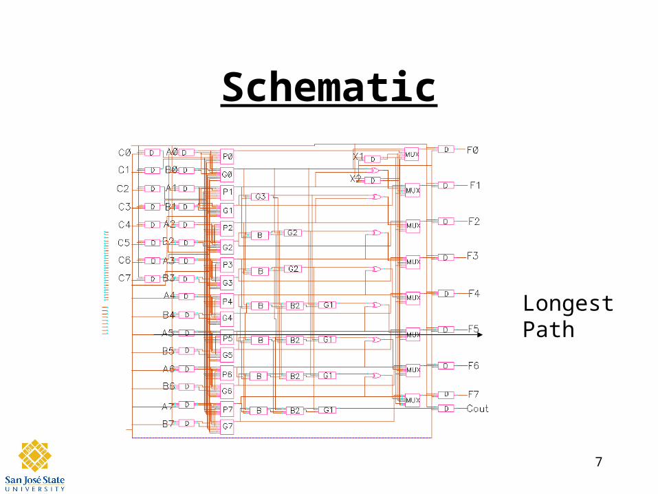
Schematic
Longest Path

8
Longest Path Calculations
Note: All widths are in microns and capacitances in fFPropagation delay/ Logic level : 5ns/16
9
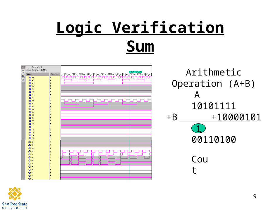
Logic VerificationSum
Arithmetic Operation (A+B)
A 10101111+B +10000101 00110100
Cout
1
10
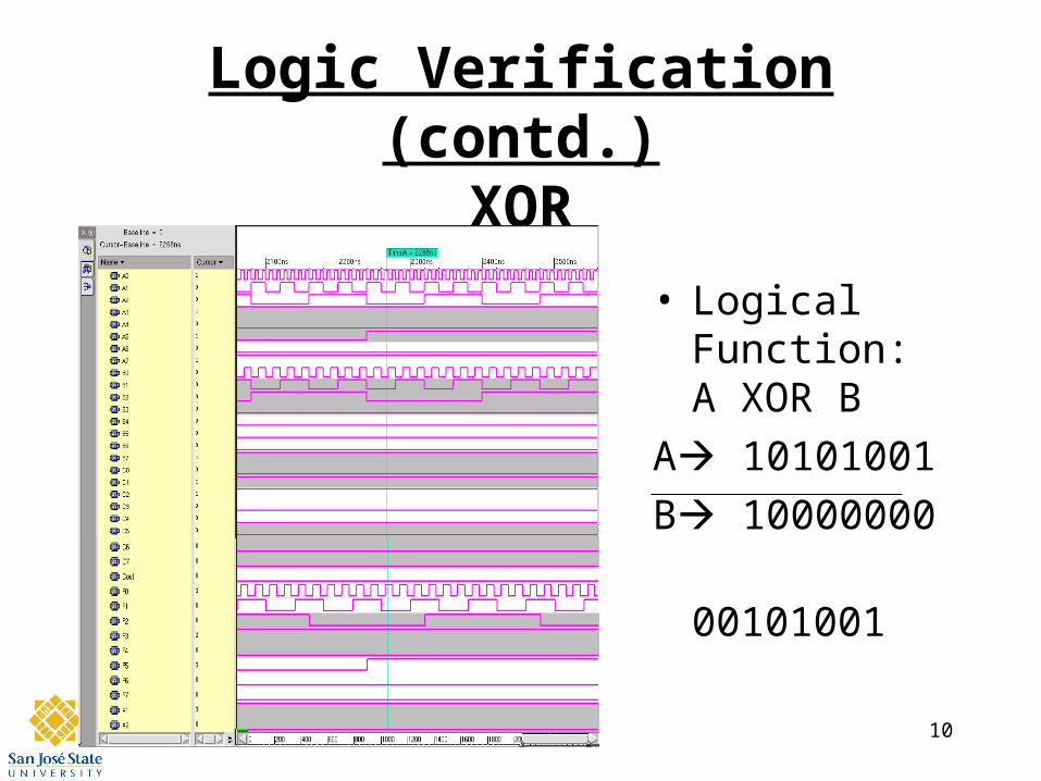
Logic Verification (contd.)XOR
• Logical Function: A XOR B
A 10101001
B 10000000
00101001
11
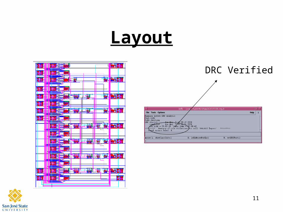
Layout
DRC Verified

12
Layout verification

13
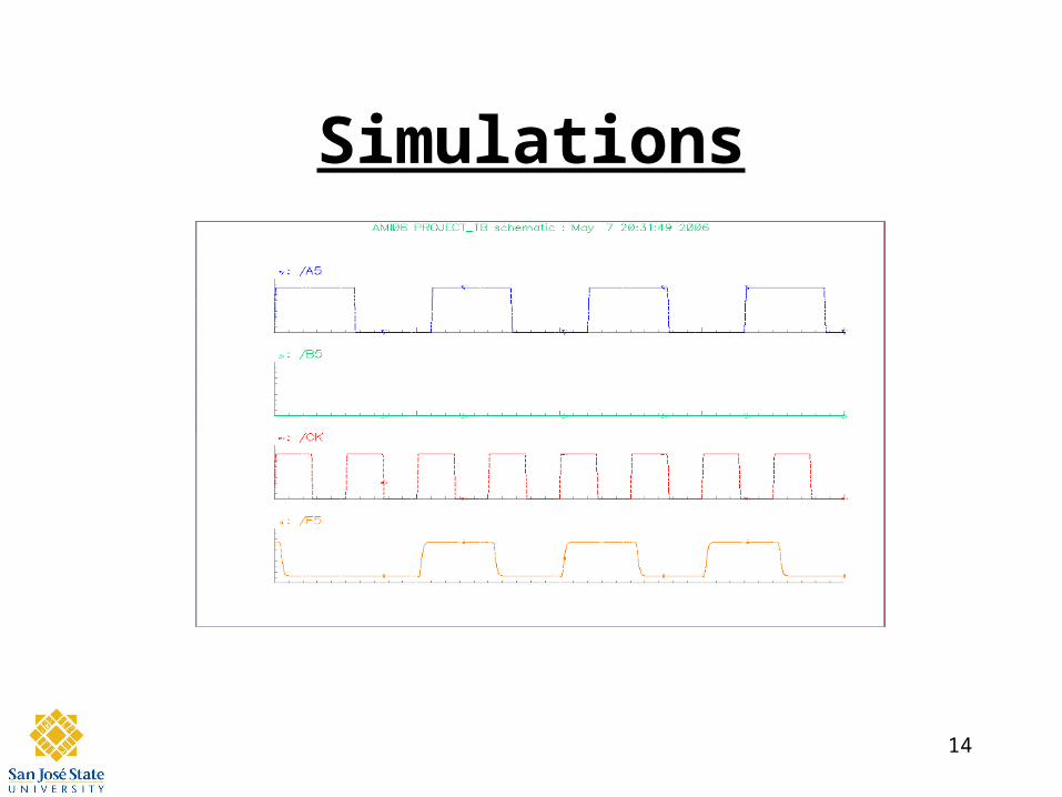
Test Bench
14
Simulations
15
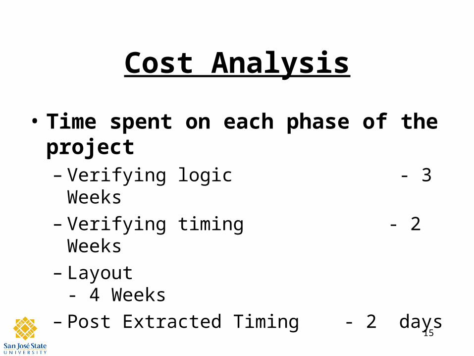
Cost Analysis
• Time spent on each phase of the project– Verifying logic - 3 Weeks– Verifying timing - 2 Weeks– Layout - 4 Weeks– Post Extracted Timing - 2 days

16
Lessons Learnt
• Planning is very important.
• Start early and have clear estimation of the work to be done.
• Give more time for the layout stage.

17
Summary
• Designed and tested almost all the design units learnt in the class.
• This design can be modified to be used in higher order bit ALU’s and more functions.
• We designed 8-Bit ALU working at 200 MHz speed ,driving 20fF load.
18
Acknowledgements
• Thanks to Cadence Design Systems for the VLSI lab and Remote Login.
• Thanks to Hummingbird for remote login.
• Thanks to Professor David Parent for his valuable guidance.