1 5-bit flash encoder nam van do, dave flores, shawn smith advisor: dr. david parent december 6,...
Post on 20-Dec-2015
217 views
TRANSCRIPT
1
5-bit Flash Encoder
Nam Van Do, Dave Flores, Shawn Smith
Advisor: Dr. David Parent
December 6, 2004

2
Agenda
• Abstract• Introduction
– Why– Simple Theory– Background information (Literature Review)
• Summary of Results• Project (Experimental) Details• Results• Conclusions
3
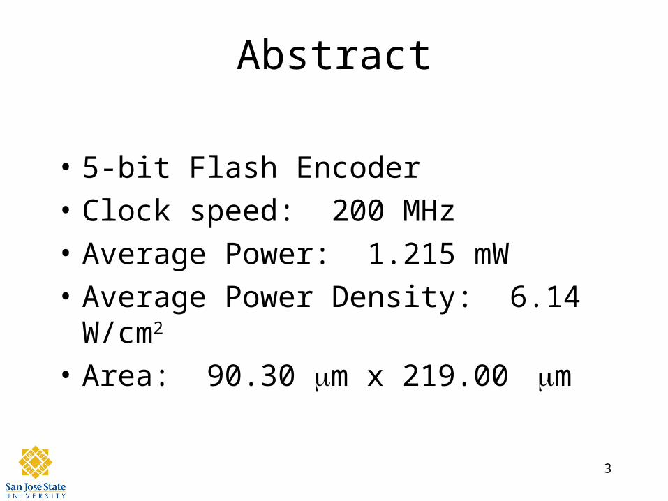
Abstract
• 5-bit Flash Encoder
• Clock speed: 200 MHz
• Average Power: 1.215 mW
• Average Power Density: 6.14 W/cm2
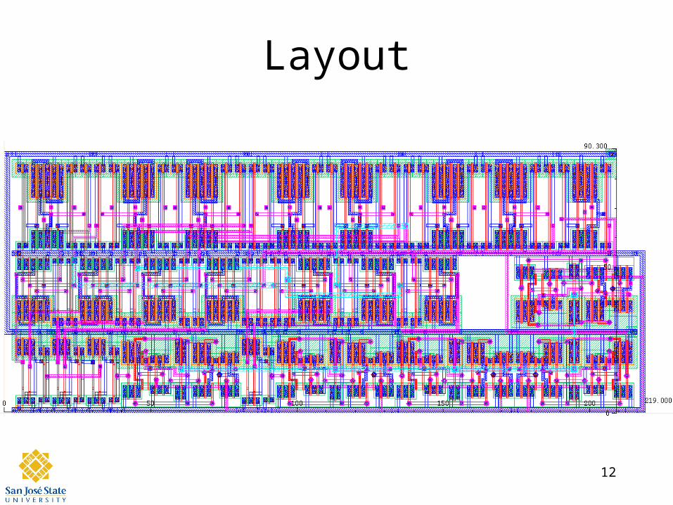
• Area: 90.30 m x 219.00 m
4
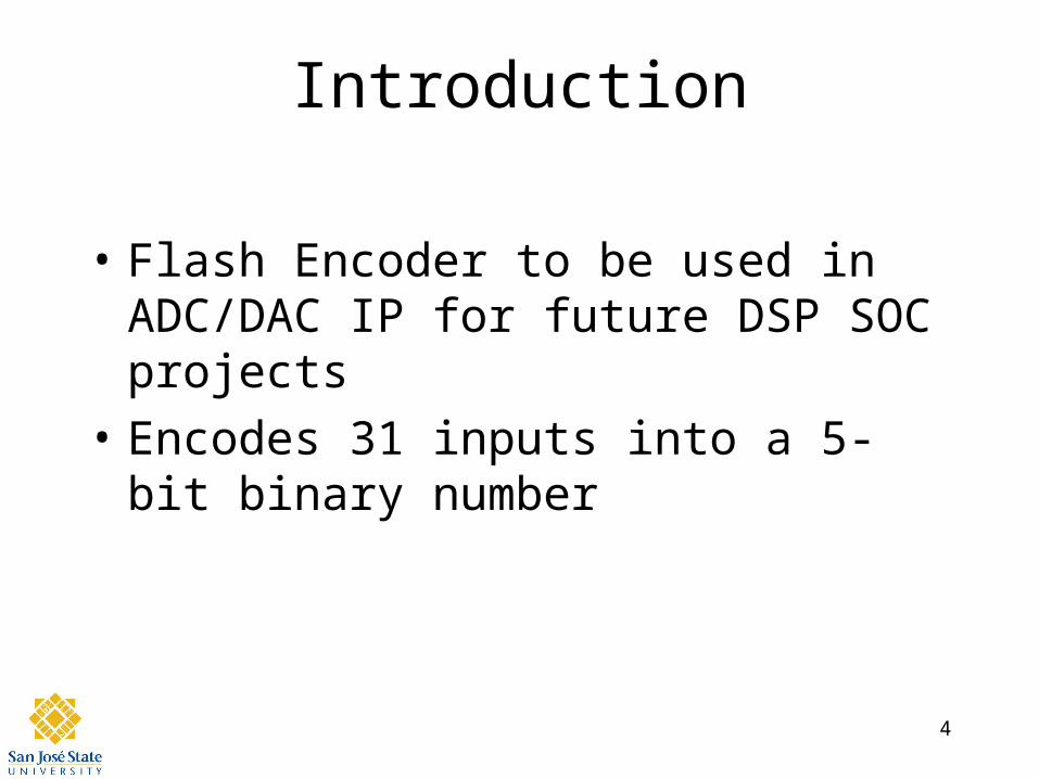
Introduction
• Flash Encoder to be used in ADC/DAC IP for future DSP SOC projects
• Encodes 31 inputs into a 5-bit binary number
5
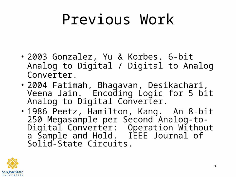
Previous Work
• 2003 Gonzalez, Yu & Korbes. 6-bit Analog to Digital / Digital to Analog Converter.
• 2004 Fatimah, Bhagavan, Desikachari, Veena Jain. Encoding Logic for 5 bit Analog to Digital Converter.
• 1986 Peetz, Hamilton, Kang. An 8-bit 250 Megasample per Second Analog-to-Digital Converter: Operation Without a Sample and Hold. IEEE Journal of Solid-State Circuits.
6
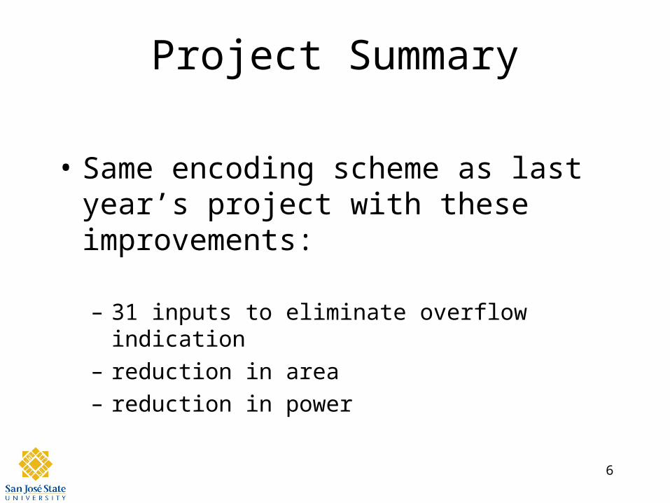
Project Summary
• Same encoding scheme as last year’s project with these improvements:
– 31 inputs to eliminate overflow indication
– reduction in area
– reduction in power
7
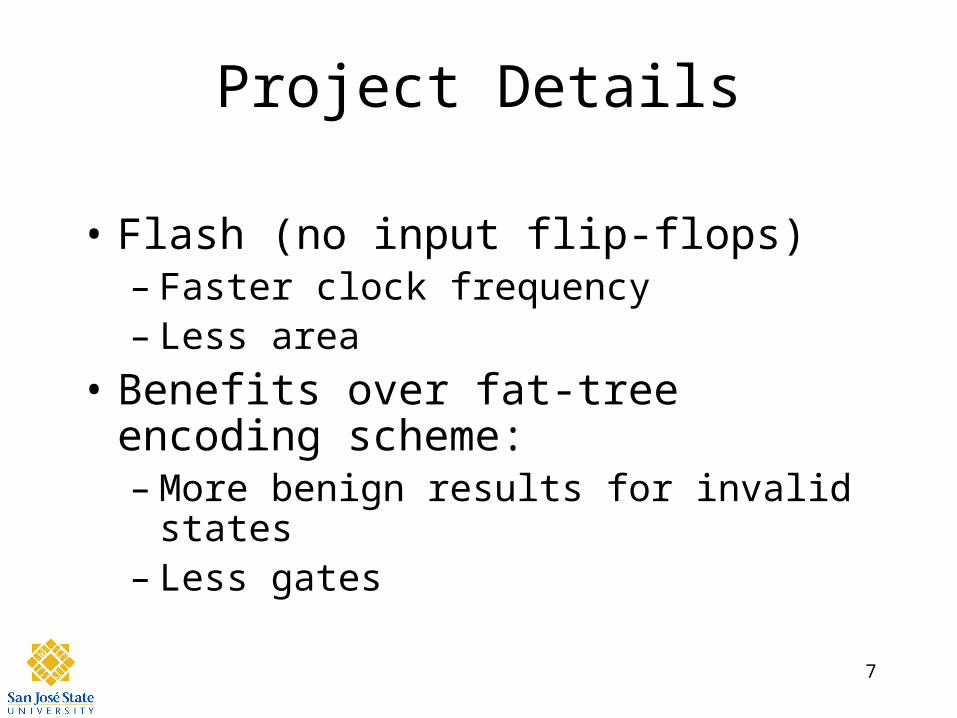
Project Details
• Flash (no input flip-flops)– Faster clock frequency– Less area
• Benefits over fat-tree encoding scheme:– More benign results for invalid states– Less gates
8
Project Details
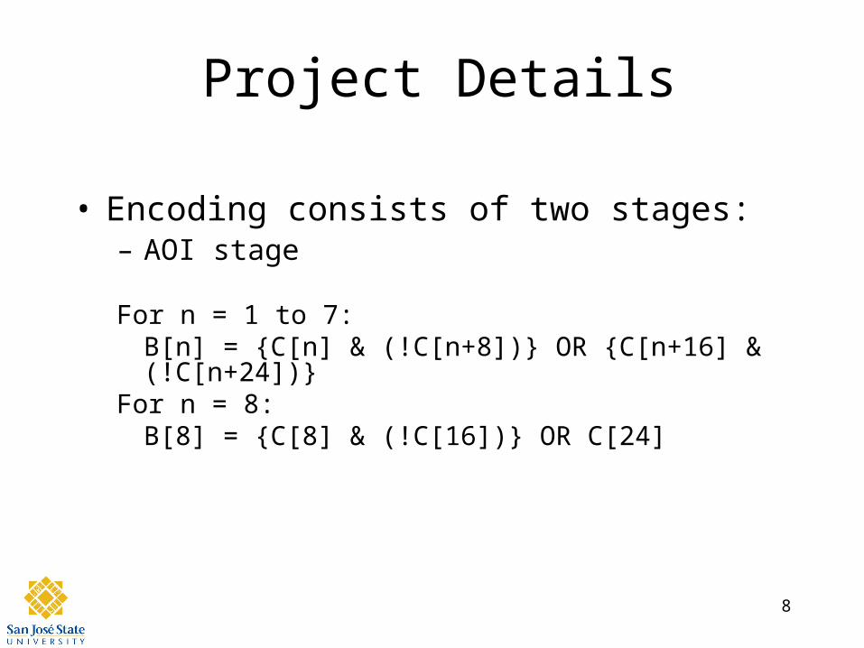
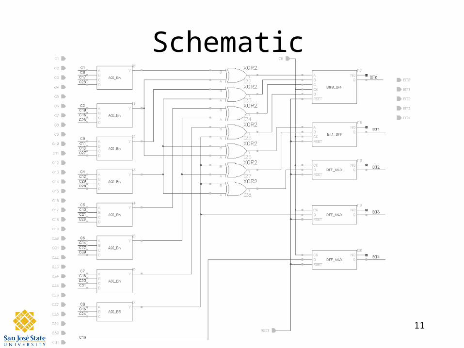
• Encoding consists of two stages:– AOI stage
For n = 1 to 7:B[n] = {C[n] & (!C[n+8])} OR {C[n+16] & (!C[n+24])}
For n = 8:B[8] = {C[8] & (!C[16])} OR C[24]
9
Project Details
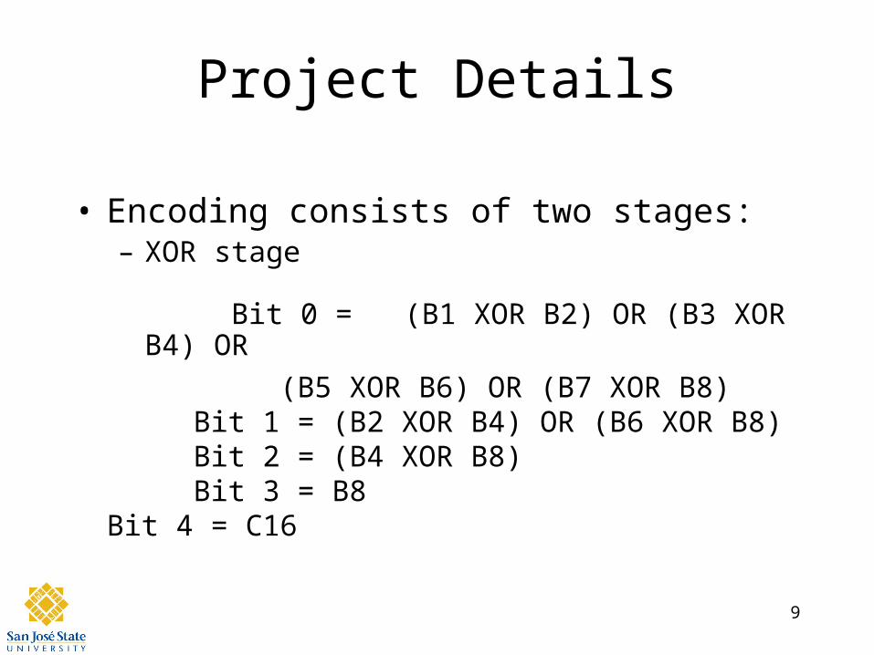
• Encoding consists of two stages:– XOR stage
Bit 0 = (B1 XOR B2) OR (B3 XOR B4) OR
(B5 XOR B6) OR (B7 XOR B8) Bit 1 = (B2 XOR B4) OR (B6 XOR B8) Bit 2 = (B4 XOR B8) Bit 3 = B8
Bit 4 = C16
10
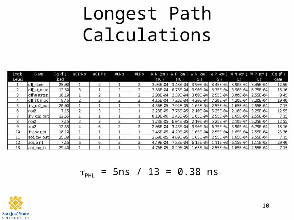
Longest Path Calculations
Logic Gate Cg (fF) #CDNs #CDPs #LNs #LPs WN (cm) WP (cm) WN (cm) WP (cm) WN (cm) WP (cm) Cg (fF)Level load (HC) (HC) (S) (S) (L) (L) gate
1 dff_slave 25.00 1 2 1 2 3.94E-04 3.43E-04 3.90E-04 3.45E-04 3.90E-04 3.45E-04 12.502 dff_st_mux 12.50 3 1 2 2 3.86E-04 6.73E-04 3.90E-04 6.75E-04 3.90E-04 6.75E-04 18.103 dff_master 18.10 1 2 1 2 2.98E-04 2.59E-04 3.00E-04 2.55E-04 3.00E-04 2.55E-04 9.454 dff_st_mux 9.45 2 2 2 2 4.15E-04 7.23E-04 4.20E-04 7.20E-04 4.20E-04 7.20E-04 19.405 inv_or2_out 20.00 1 1 1 1 4.56E-05 7.94E-05 1.65E-04 2.55E-04 1.65E-04 2.55E-04 7.156 nor2 7.15 2 3 2 1 2.23E-05 7.76E-05 2.10E-04 5.25E-04 2.10E-04 5.25E-04 12.557 inv_or2_out 12.55 1 1 1 1 8.19E-06 1.43E-05 1.65E-04 2.55E-04 1.65E-04 2.55E-04 7.158 nor2 7.15 2 3 2 1 1.73E-05 6.04E-05 2.10E-04 5.25E-04 2.10E-04 5.25E-04 12.559 xor2 12.55 4 6 2 2 2.08E-04 3.43E-04 3.90E-04 6.75E-04 3.90E-04 6.75E-04 18.1010 inv_xor_in 18.10 1 1 1 1 2.46E-05 4.29E-05 1.65E-04 2.55E-04 1.65E-04 2.55E-04 25.3011 aoi_inv_out 25.30 1 1 1 1 2.69E-05 4.69E-05 1.65E-04 2.55E-04 1.65E-04 2.55E-04 7.1512 aoi_b[n] 7.15 6 6 2 2 4.49E-04 7.83E-04 6.15E-04 1.11E-03 6.15E-04 1.11E-03 29.4013 aoi_inv_in 29.40 1 1 1 1 4.76E-05 8.29E-05 1.65E-04 2.55E-04 1.65E-04 2.55E-04 7.15
PHL = 5ns / 13 = 0.38 ns
11
Schematic
12
Layout
13
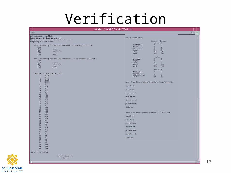
Verification

14
Verification
15
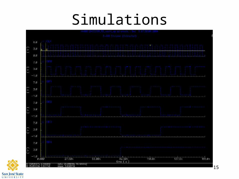
Simulations
16
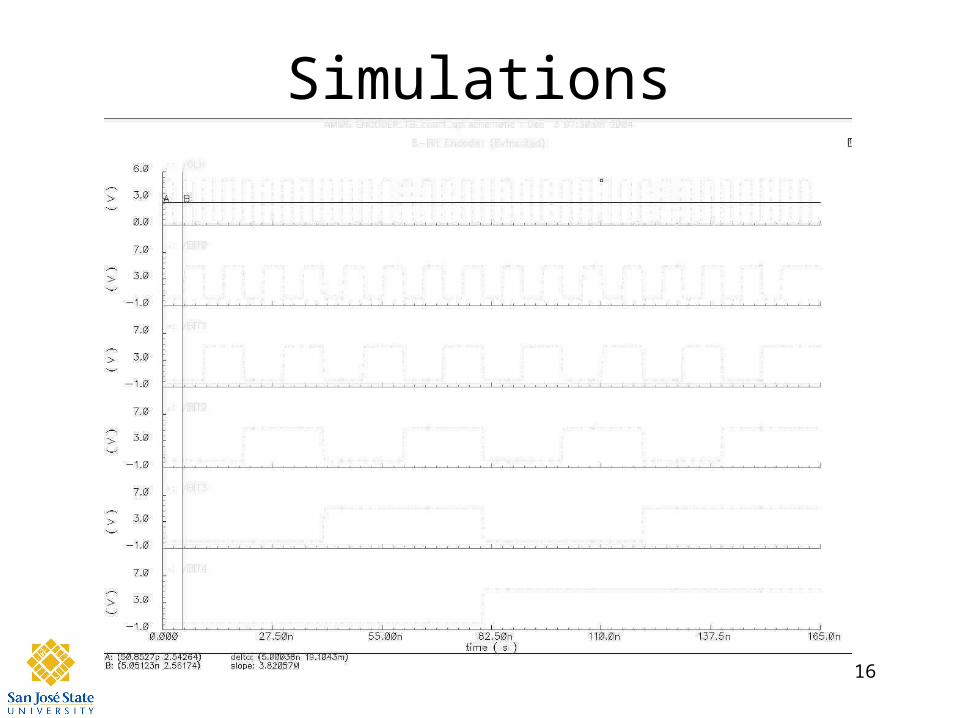
Simulations
17
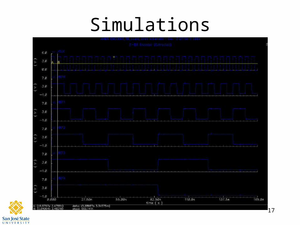
Simulations
18
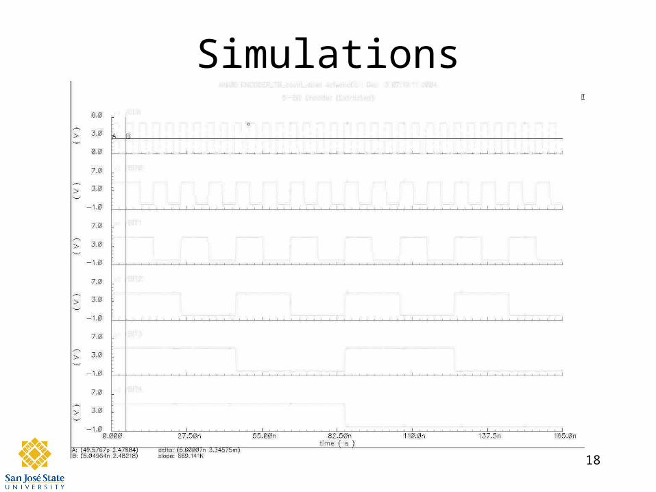
Simulations
19
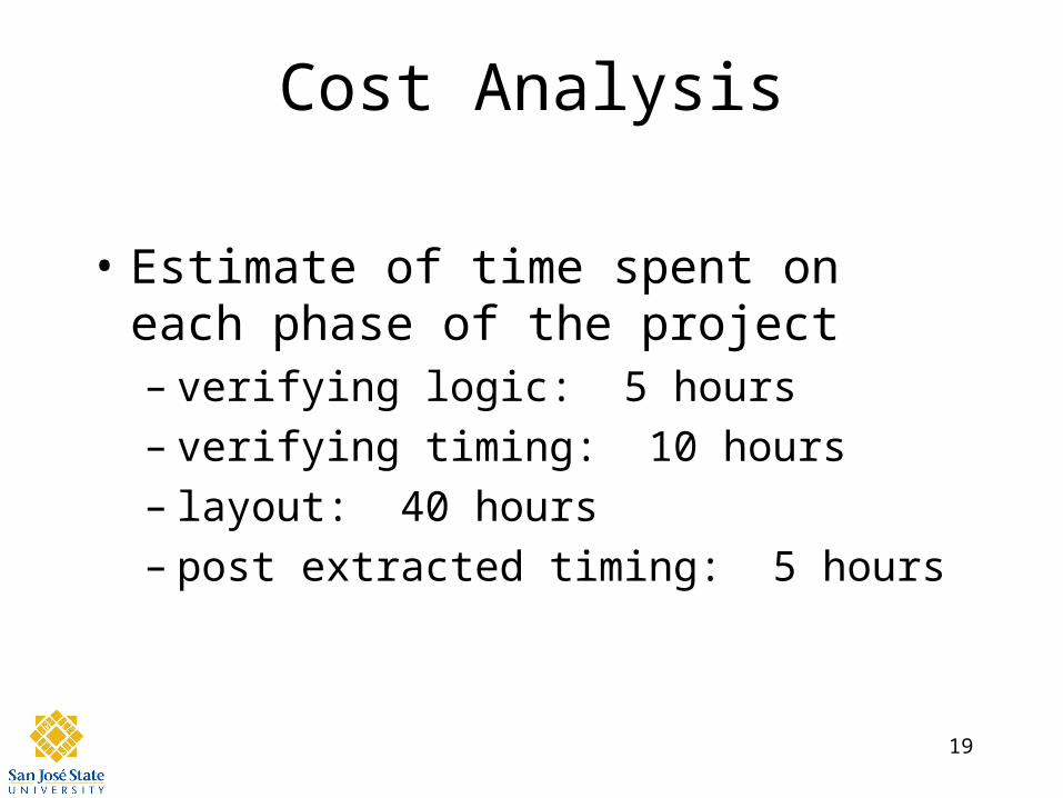
Cost Analysis
• Estimate of time spent on each phase of the project– verifying logic: 5 hours– verifying timing: 10 hours– layout: 40 hours– post extracted timing: 5 hours
20
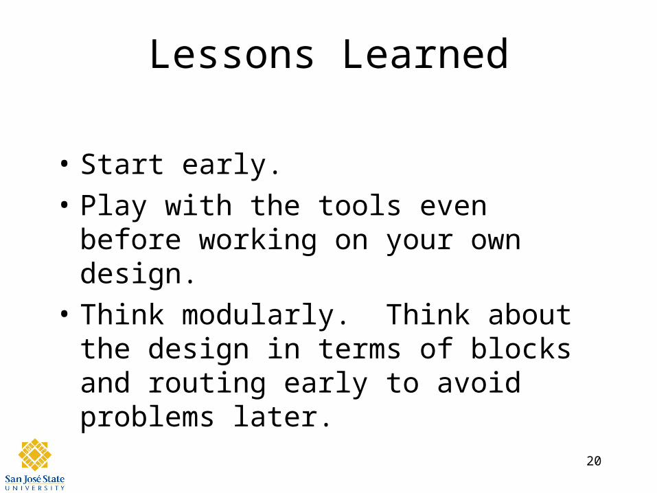
Lessons Learned
• Start early.
• Play with the tools even before working on your own design.
• Think modularly. Think about the design in terms of blocks and routing early to avoid problems later.
21
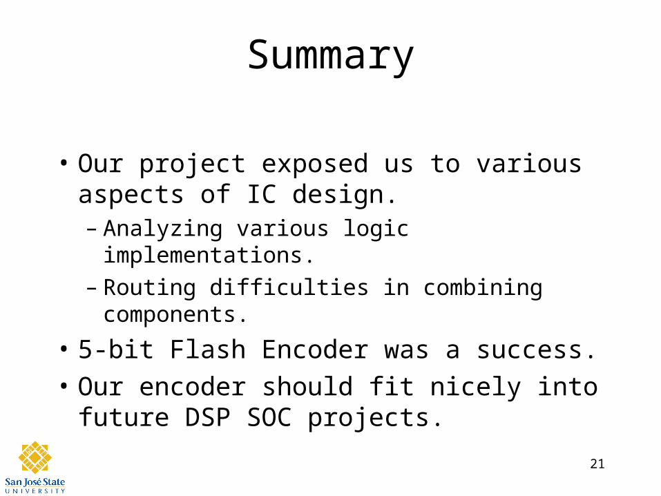
Summary
• Our project exposed us to various aspects of IC design.– Analyzing various logic implementations.– Routing difficulties in combining components.
• 5-bit Flash Encoder was a success.
• Our encoder should fit nicely into future DSP SOC projects.
22
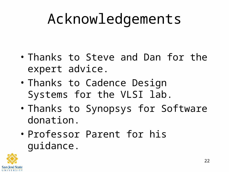
Acknowledgements
• Thanks to Steve and Dan for the expert advice.
• Thanks to Cadence Design Systems for the VLSI lab.
• Thanks to Synopsys for Software donation.
• Professor Parent for his guidance.