06560348
DESCRIPTION
implant poweringTRANSCRIPT

IEEE TRANSACTIONS ON INDUSTRIAL ELECTRONICS, VOL. 61, NO. 5, MAY 2014 2225
Wireless Power Transmission With Self-RegulatedOutput Voltage for Biomedical Implant
Dukju Ahn and Songcheol Hong, Member, IEEE
Abstract—This paper presents a wireless power transfer (WPT)system for powering implantable biomedical devices; the systemis configured to achieve high efficiency even with CMOS switchesand printed-circuit-board pattern coils and to maintain constantoutput voltage against coupling and loading variations withoutany additional blocks. It is shown that the parallel-resonant trans-mitter (TX) and receiver (RX) topology is advantageous for highefficiency even with lossy but compact components. In addition,the output voltage of the topology is insensitive to coupling and/orloading variations if the operating frequency is automaticallyadjusted according to coupling variations. A parallel-resonantclass-D oscillator TX is developed to track the optimum operatingfrequency for the constant output voltage. The operating distancefor the constant output voltage is also extended using a novelresonator structure, which contains two resonating coils. Theseproposed schemes allow a compact, efficient, and robust wirelesspower system. Maximum power of 174 mW can be transmittedwith 63% overall efficiency.
Index Terms—Biomedical implant, CMOS transmitter (TX),coupled resonator, inductive link, inductive power, voltage regu-lation, wireless power transfer (WPT).
I. INTRODUCTION
AMONG the applications of wireless power transmissiontechnology, wireless powering of implanted biomedical
devices is one of the most important subjects. [1]–[10]. Theprimitive method of power supply for implanted devices wasto insert power cables through skin holes. However, such aninvasive method is subject to infections through the skin holes.Therefore, implanted devices should be powered wirelessly toavoid infection problems.
Fig. 1 illustrates the overall block diagram of a wirelesspower system for biomedical implants. Since most of the cir-cuits and systems require constant supply voltage for stable op-eration, the receiver (RX) load voltage should be stable over thevarying operating conditions. However, as the distance betweenthe outside parallel-resonant transmitter (TX) and the implantedRX is varied, the transferred power will change accordingly.
Manuscript received July 10, 2012; revised February 27, 2013 andApril 25, 2013; accepted June 24, 2013. Date of publication July 16, 2013;date of current version October 18, 2013. This work was supported by theNational Research Foundation of Korea under Grant 2005-2001282 funded bythe Ministry of Science, ICT & Future Planning.
D. Ahn was with the Department of Electrical Engineering, Korea AdvancedInstitute of Science and Technology, Daejeon 305-701, Korea. He is nowwith the School of Electrical and Computer Engineering, Georgia Institute ofTechnology, Atlanta, GA 30308 USA (e-mail: [email protected]).
S. Hong is with the Department of Electrical Engineering, Korea Ad-vanced Institute of Science and Technology, Daejeon 305-701, Korea (e-mail:[email protected]).
Color versions of one or more of the figures in this paper are available onlineat http://ieeexplore.ieee.org.
Digital Object Identifier 10.1109/TIE.2013.2273472
Fig. 1. Overall block diagram of wireless power system for biomedicalimplants. A relatively constant input voltage to the RX regulator is desiredregardless of coupling and loading variations.
RX regulators may provide constant RX load voltage under dis-tance variation by trimming the excessive RX rectifier voltage.However, the input voltage to the RX regulator should not betoo high compared with the required RX load voltage. Highinput voltage to regulators may result in device breakdown.In addition, excess input power may generate heat and reduceefficiency because the power exceeding the required amountwill be dissipated uselessly in the RX regulator [5]. Therefore,a relatively constant input voltage to the RX regulator is desiredregardless of coupling and load variations.
There have been many efforts to obtain the constant outputvoltage. References [1], [2], and [11] achieved constant outputvoltage under coupling and loading variations for high-powerapplication (10 W–2 kW). However, those implementationsrequire lossy, complex, and bulky additional components andpower-consuming active devices for feedback or communica-tion. Although such bulky and power-consuming componentsare acceptable for high-power systems such as [1], [2], and [11],these are not allowed in low-power lightweight applications.References [3], [4], [12], and [23] exhibit relatively constantoutput voltage under coupling variation. However, the variationof output voltage is relatively high, and the distance range forconstant output is limited. In addition, the effect of load resis-tance variation on output voltage is not discussed. Reference[5] employs a communication link to notify the TX of the RX’spower demand. Upon the receipt of the RX’s power demand,the TX power amplifier (PA) supply voltage is adjusted using adc–dc converter. This coarsely regulates the RX rectifier output(or regulator input). In this way, the input voltage to the RXregulator does not exceed the required load voltage by toomuch, and the power loss at the RX regulator is kept belowa reasonable level under the coupling or loading variations.However, the scheme [5] requires communication functionality,a power control unit, and a wide-output-range dc/dc converter,
0278-0046 © 2013 IEEE

2226 IEEE TRANSACTIONS ON INDUSTRIAL ELECTRONICS, VOL. 61, NO. 5, MAY 2014
all of which increase the system cost and complexity. Thepower consumption at such active blocks is not allowed for low-power system.
In addition to a stable output voltage, the system efficiencyshould be high, whereas the utilized components should becompact. Most of the previous wireless power systems haverelied on discrete power MOSFET as a PA switch due to itslow on-resistance compared with that of an integrated CMOSswitch. In the case of [5] and [8], an on-chip CMOS circuit isused to implement the TX control loop, whereas the externalpower MOSFET and the gate driver are used for the PA switch.Integrating the power MOSFET into the on-chip CMOS wouldreduce system cost and complexity. Reference [4] utilized inte-grated CMOS transistors for its PA switch. However, the widthof the CMOS switch could not be increased indefinitely becausethe gate input capacitance Cg is also increased with the transis-tor width. Large gate capacitance increases the power consump-tion at the gate driver. Due to this tradeoff, it was not possible tosufficiently reduce the on-resistance of the PA switch (∼5 Ω).As a result, the TX coil was designed to be as large as ∼6 μHin order to minimize the effect of on-resistance [4].
Unlike previous works, the proposed TX structure utilizeson-chip CMOS switches for better integration. Moreover, amuch smaller coil (∼500 nH), which can be patterned on aprinted circuit board (PCB), is used without losing efficiency.As a result, a compact but efficient system is realized. To stabi-lize the output voltage against coupling and loading variations,we propose the parallel-resonant TX and RX topology thatoscillates at the frequency at which constant output is obtained.This scheme does not require any bulky or power-consumingexternal devices. We also propose a novel two-coil resonator toextend the distance limit up to which the constant output voltageis obtained.
This paper is organized as follows. Section II compares theseries- and the parallel-resonant topologies and explains thereason for the higher efficiency at parallel-resonant topologyunder the component loss and size constraints. Section IIIinvestigates the output voltage sensitivity against coupling andloading variations and proposes schemes to stabilize the outputvoltage. Section IV proposes a novel resonator structure con-sisting of two parallel coils in order to extend the constant-output distance range. Section V presents the measurementresults. Conclusions are drawn in Section VI.
II. RESONANCE TOPOLOGY SELECTION
FOR HIGH EFFICIENCY
Practically, there are limitations on maximum obtainableefficiency of wireless power transfer (WPT) due to componentlosses. Notably, the on-resistance of a CMOS switch and theparasitic resistances of PCB coils reduce the efficiency. Thissection proposes that the parallel-resonant TX and RX topologyis efficient under the given component losses.
A. Generalized Equivalent Circuit of WPT
Fig. 2(a) illustrates an equivalent circuit of a WPT system.The effect of magnetic coupling with an RX is represented as
Fig. 2. (a) Equivalent circuit of the WPT system. (b) Coupling effect betweenTX and RX can be represented as an equivalent impedance value calledreflected impedance. The reflected resistance should be high compared withthe TX parasitic resistance in order to obtain high efficiency.
an equivalent impedance value in a TX circuit called reflectedimpedance. The power consumed in the reflected resistance isequal to the actual power transferred to the RX. Therefore, thereal part of the reflected impedance should be sufficiently largerthan the parasitic resistance of the TX RTX in order to obtainhigh efficiency [13] and [14].
For a series-resonant RX, the reflected impedance at RXresonant frequency ω0 is
Zreflected = k2ω0L1QRX (1)
where ω0 is the resonant frequency of the RX LC tank, QRX
is the loaded-Q of the RX, and k is the magnetic couplingcoefficient. For the parallel-resonant RX, the reflected imped-ance is
Zreflected = k2ω0L1(QRX − j). (2)
In both cases, the RX loaded-Q and the TX inductanceshould be large in order to obtain high reflected resistance underthe given coupling coefficient.
B. TX Resonance Topology
TX resonance topology is selected between series and par-allel resonances by considering the achievable PA efficiencyunder the given component loss constraints.
For a system driven by a series-resonant class-D amplifier,the equivalent circuit is shown in Fig. 3. Its efficiency is
eff =1
1 + RDSon
Rreflected
(3)
where RDSon is the on-resistance of the TX CMOS switch,and Rreflected is the real part of the reflected impedance of theRX [15]. The on-resistance of an nMOS transistor whose widthand length are 2880 and 0.35 μm, respectively, is simulated asRDSon = 1.7 Ω. Rreflected can be evaluated using (1) or (2)under the given k, QRX, and L1. k and QRX are limited bygeometry and RX power consumption, whose values are around0.1 and 11.9 in this paper. Equation (1) or (2) implies that theTX coil L1 should be large in order to obtain high Rreflected

AHN AND HONG: WIRELESS POWER TRANSMISSION WITH OUTPUT VOLTAGE FOR BIOMEDICAL IMPLANT 2227
Fig. 3. (a) System driven by a series-resonant class-D PA. (b) Equivalentcircuit represented by reflected impedance.
in (3). However, there are practical geometric limitations on themaximum obtainable TX inductance. Moreover, the couplingcoefficient between TX and RX is gradually reduced when theturn number of the coils is increased because the inner turndiameter is reduced as the turn number is increased. Therefore,the increase in TX inductance does not provide increased re-flected resistance beyond a certain TX inductance value. Undersuch constraints, TX inductance values of 614 and 1270 nH areobtained with turn numbers of 3 and 5, respectively, for an outersquare side of 30 mm.
For a five-turn coil, reflected resistance Rreflected is at most7.6 Ω. Substituting RDSon and Rreflected into (3), the efficiencyof the PA is 1/(1 + 1.7/7.6) = 81.7%, which is somewhat low.If the three-turn coil is used, the calculated PA efficiency wouldbe at most 68.3%. This is because the magnitudes of RDSon
and Rreflected are quite similar and, therefore, a similar amountof power is dissipated in each resistor.
On the other hand, for a parallel-resonant TX, the effect ofthe CMOS switch RDSon is not that serious. Fig. 4(a) illustratesa system driven by a parallel-resonant class-D PA. To findthe efficiency of the parallel-resonant class-D PA, the reflectedresistance shown in Fig. 4(b) is transformed to a parallel resistorusing the relationship of
RP∼= ω2
0L21
Rreflected(4)
as illustrated in Fig. 4(c) under the condition of Rreflected �ω0L1. The efficiency of the parallel-resonant class-D PA is [15]
eff =1
1 + π2
2 × RDSon
RP
. (5)
Substituting RDSon = 1.7 Ω and RP∼= 259 Ω into (5), the
calculated PA efficiency is ∼96.9%, which is higher than thatof the series-resonant PA. This is because reflected resistanceRreflected is “boosted” into RP as a result of the series-to-parallel transformation. Although the orders of magnitude ofRDSon and Rreflected are the same, much higher power is
Fig. 4. (a) System driven by a parallel-resonant class-D PA. (b) Equivalentcircuit represented with the reflected resistance. (c) Reflected resistance istransformed to a parallel resistor RP .
consumed in Rreflected than in RDSon because of the largeresonant current in the LC tank, yielding the higher efficiency.
In conclusion, the parallel-resonant TX can achieve highefficiency even with high-RDSon CMOS switches. In addition,the parallel-resonant TX is advantageous in terms of powerregulation and circuit implementation, which will be discussedin Section III.
C. RX Resonance Topology
The RX resonance topology should be selected in such a waythat the loaded-Q of the RX is high in order to obtain highreflected resistance.
The loaded-Q factors of the series- and the parallel-resonantcircuits are
QRX,series =ω0L2
RL(6)
QRX,parallel =RL
ω0L2(7)
respectively. Load resistance RL is determined by the powerdemand of the RX. A load resistance of 122.5 Ω consumes100 mW under 3.5-V load voltage. The maximum RX induc-tance obtainable is ∼2 μH for the dimensions of 20 mm ×20 mm.
2228 IEEE TRANSACTIONS ON INDUSTRIAL ELECTRONICS, VOL. 61, NO. 5, MAY 2014
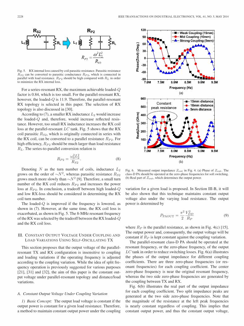
Fig. 5. RX internal loss caused by coil parasitic resistance. Parasitic resistanceRS2 can be converted to parasitic conductance RP2, which is connected inparallel with load resistance. RP2 should be high compared with RL in orderto minimize the RX internal loss.
For a series-resonant RX, the maximum achievable loaded-Qfactor is 0.84, which is too small. For the parallel-resonant RX,however, the loaded-Q is 11.9. Therefore, the parallel-resonantRX topology is selected in this paper. The selection of RXtopology is also discussed in [30].
According to (7), a smaller RX inductance L2 would increasethe loaded-Q and, therefore, would increase reflected resis-tance. However, too small RX inductance increases the RX coilloss at the parallel-resonant LC tank. Fig. 5 shows that the RXcoil parasitic RS2, which is originally connected in series withthe RX coil, can be converted to a parallel resistance RP2. Forhigh efficiency, RP2 should be much larger than load resistanceRL. The series-to-parallel conversion relation is
RP2 =ω20L
22
RS2. (8)
Denoting N as the turn number of coils, inductance L2
grows on the order of ∼N2, whereas parasitic resistance RS2
grows much more slowly than ∼N2 [9]. Therefore, a small turnnumber of the RX coil reduces RP2 and increases the powerloss at RP2. In conclusion, a tradeoff between high loaded-Qand low RX-loss should be considered in determining the RXcoil turn number.
The loaded-Q is improved if the frequency is lowered, asshown in (7). However, at the same time, the RX coil loss isexacerbated, as shown in Fig. 5. The 8-MHz resonant frequencyof the RX was selected by the tradeoff between the RX loaded-Qand the RX coil loss.
III. CONSTANT OUTPUT VOLTAGE UNDER COUPLING AND
LOAD VARIATIONS USING SELF-OSCILLATING TX
This section proposes that the output voltage of the parallel-resonant TX and RX configuration is insensitive to couplingand loading variations if the operating frequency is adjustedaccording to the coupling variation. While the idea of split fre-quency operation is previously suggested for various purposes[21], [31] and [32], the aim of this paper is the constant out-put voltage under parallel-resonant topology and distance/loadvariations.
A. Constant Output Voltage Under Coupling Variation
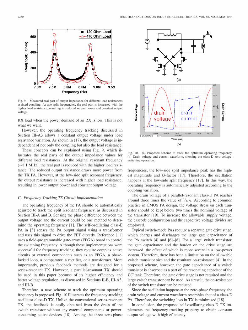
1) Basic Concept: The output load voltage is constant if theoutput power is constant for a given load resistance. Therefore,a method to maintain constant output power under the coupling
Fig. 6. Measured output impedance Zout in Fig. 4. (a) Phase of Zout. Theclass-D PA should be operated at the zero-phase frequencies for soft switching.(b) Real part of Zout, which determines the output power.
variation for a given load is proposed. In Section III-B, it willbe also shown that this technique maintains constant outputvoltage also under the varying load resistance. The outputpower is determined by
PPAOUT =π2
2
V 2DD
RP(9)
where RP is the parallel resistance, as shown in Fig. 4(c) [15].The output power and, consequently, the output voltage will beconstant if RP is kept constant against the coupling variation.
The parallel-resonant class-D PA should be operated at theresonant frequency, or the zero-phase frequency, of the outputLC tank in order to reduce switching losses. Fig. 6(a) illustratesthe phases of the output impedance for different couplingcoefficients. There are three zero-phase frequencies (or res-onant frequencies) for each coupling coefficient. The centerzero-phase frequency is near the original resonant frequency,whereas the two side zero-phase frequencies are generated bythe coupling between TX and RX.
Fig. 6(b) illustrates the real part of the output impedancefor each coupling coefficient. Two split impedance peaks aregenerated at the two side zero-phase frequencies. Note thatthe magnitude of the resistance at the left peak frequenciesis nearly constant regardless of coupling. This implies thatconstant output power, and thus the constant output voltage,

AHN AND HONG: WIRELESS POWER TRANSMISSION WITH OUTPUT VOLTAGE FOR BIOMEDICAL IMPLANT 2229
Fig. 7. Equivalent circuit to find PA output admittance for parallel-resonantTX and RX. Constant reflected admittance can be obtained under couplingvariation if the operating frequency tracks the split frequencies automatically.
will be obtained if the excitation frequency tracks the split peakfrequencies when the coupling is changed.
2) Fixed-Frequency Operation: If the operating frequencyis fixed at the original resonant frequency ω0, the parallel outputconductance 1/RP can be calculated using Fig. 4, resulting in
1
RP
∼= Rreflected
ω20L
21
∼= k21
ω0L1QRX. (10)
Substituting (10) into (9) gives the output power
PPAOUT =π2
2V 2DDk2
1
ω0L1QRX (11)
which is proportional to ∼k2. Therefore, the output powerat fixed-frequency operation is very sensitive to couplingvariation.
3) Tracking Optimum Frequency According to Coupling:As discussed in Section III-A1, constant output impedance canbe obtained under coupling variation if the system operatesat the split resonant frequency. The split resonant frequenciesare found using the procedures outlined in [14], [16], or [17],resulting in
ω =ω0√1 + k
, and ω =ω0√1− k
. (12)
The KVL equation in Fig. 7 can be written as
1
jωC1(I1 − IS) + jωL1I1 + jkω
√L1L2I2 =0 (13.a)
jkω√L1L2I1 + jωL2I2 +
RL
1 + jωRLC2I2 =0. (13.b)
The output admittance in Fig. 7 at the low-side split resonantfrequency is obtained by evaluating YOUT = jωC1IS/(IS −I1), resulting in
YOUT|ω=ω0√1+k
=jω0C1
(1− 1/k − jQRX/
√1 + k
)√1 + k
((1− 1
k
)2+
Q2RX
1+k
) (14)
which is reduced to
YOUT∼= ω0C1
QRX=
1
RP(15)
under the condition of
k2 � 1 + k
Q2RX
. (16)
Fig. 8. Equivalent circuit to find PA output resistance for series-resonant TX.Unlike that of its parallel-resonant TX counterpart, the output voltage of theseries-resonant TX is sensitive to coupling variation.
Therefore, the admittance becomes independent of couplingwhen the coupling and the RX-Q are sufficiently high. Sub-stituting (15) into (9) gives the output power of a class-Damplifier. The induced voltage to load resistance becomesconstant if the output power is constant under the given loadresistance. The induced voltage can be found using (9) and (15),resulting in
VLOAD|ω=ω0√1+k
= VDD
√π2
2
C1
C2(17)
which is independent of the coupling coefficient. Therefore,the parallel-resonant TX and RX system, such as that shownin Fig. 7, exhibits constant output voltage when the operatingfrequency is adjusted to the resonant frequencies in (12).
Note that, unlike that of the parallel-resonant TX, the outputvoltage of series-resonant TX varies under the coupling vari-ation even if frequency tracking is used as in (12). Fig. 8(a)illustrates the equivalent circuit to find the PA output resistancefor series-resonant TX. The output resistance at the low-sidesplit frequency is
ROUT|ω=ω0√1+k
∼= ω0L1QRX(1 + k) (18)
under the condition of k2 � ((1 + k)/(Q2RX)). Unlike the
parallel-resonant TX case in (15), the output resistance of theseries-resonant TX in (18) varies depending on the couplingeven at the split resonant frequencies.
B. Constant Output Voltage Under Load Variation
The power demand in an RX is continuously varied duringits operation. The decrease in power demand under the givensupply voltage corresponds to the increase in load resistance.Therefore, to meet the various power demands, the systemshould be able to maintain a constant output voltage even whenthe load resistance is varied.
Unfortunately, the fixed-frequency operation at the originalresonant frequency is not able to maintain a constant outputvoltage under load variations. The output voltage at an RX loadunder fixed-frequency operation can be found as
VLOAD|ω=ω0 = kRLVDD
√π2
2
1
ω0L1
1
ω0L2(19)
which implies that the output voltage is proportional to loadresistance RL. This induces an excessive output voltage at the
2230 IEEE TRANSACTIONS ON INDUSTRIAL ELECTRONICS, VOL. 61, NO. 5, MAY 2014
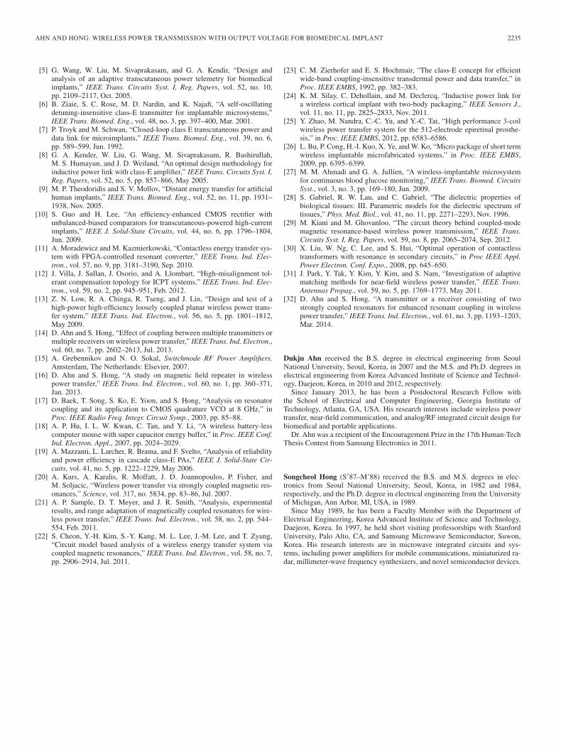
Fig. 9. Measured real part of output impedance for different load resistancesat fixed coupling. At two split frequencies, the real part is increased with thehigher load resistance, resulting in reduced output power and constant outputvoltage.
RX load when the power demand of an RX is low. This is notwhat we want.
However, the operating frequency tracking discussed inSection III-A3 allows a constant output voltage under loadresistance variation. As shown in (17), the output voltage is in-dependent of not only the coupling but also the load resistance.
These concepts can be explained using Fig. 9, which il-lustrates the real parts of the output impedance values fordifferent load resistances. At the original resonant frequency(∼8.1 MHz), the real part is reduced with the higher load resis-tance. The reduced output resistance draws more power fromthe TX PA. However, at the low-side split resonant frequency,the output resistance is increased with higher load resistance,resulting in lower output power and constant output voltage.
C. Frequency-Tracking TX Circuit Implementation
The operating frequency of the PA should be automaticallyadjusted to track the split resonant frequency, as discussed inSection III-A and B. Sensing the phase difference between theoutput voltage and the current could be one method to deter-mine the operating frequency [1]. The self-oscillating class-EPA in [3] senses the PA output signal using a transformerand uses this signal to drive the FET directly. Reference [11]uses a field-programmable gate-array (FPGA) board to controlthe switching frequency. Although these implementations weresuccessful for frequency tracking, they require complex activecircuits or external components such as an FPGA, a phase-locked loop, a comparator, a rectifier, or a transformer. Moreimportantly, previous feedback methods are designed for aseries-resonant TX. However, a parallel-resonant TX shouldbe used in this paper because of its higher efficiency andbetter voltage regulation, as discussed in Sections II-B, III-A3,and III-B.
Therefore, a new scheme to track the optimum operatingfrequency is proposed. Fig. 10 illustrates the frequency-trackingoscillator class-D TX. Unlike the conventional series-resonantTX, the feedback is easily obtained from the drain of theswitch transistor without any external components or power-consuming active devices [18]. Among the three zero-phase
Fig. 10. (a) Proposed scheme to track the optimum operating frequency.(b) Drain voltage and current waveform, showing the class-D zero-voltage-switching operation.
frequencies, the low-side split impedance peak has the high-est magnitude and Q-factor [17]. Therefore, the oscillationhappens at the low-side split frequency [17]. In this way, theoperating frequency is automatically adjusted according to thecoupling variation.
The drain voltage of a parallel-resonant class-D PA reachesaround three times the value of VDD. According to commonpractice in CMOS PA design, the voltage stress on each tran-sistor should be kept below two times the nominal voltage ofthe transistor [19]. To increase the allowable supply voltage,the cascode configuration and the capacitive voltage divider areemployed.
Typical switch-mode PAs require a separate gate drive stage,which charges and discharges the large gate capacitance ofthe PA switch [4] and [6]–[8]. For a large switch transistor,the gate capacitance and the burden on the drive stage areincreased, the effect of which is more severe in a low-powersystem. Therefore, there has been a limitation on the allowableswitch transistor size and the resultant on-resistance [4]. In theproposed scheme, however, the gate capacitance of a switchtransistor is absorbed as a part of the resonating capacitor of theLC tank. Therefore, the gate drive stage is not required and thelarge switch transistor can be used. As a result, the on-resistanceof the switch transistor can be reduced.
Since the oscillation happens at the zero-phase frequency, thedrain voltage and current waveform resembles that of a class-DPA. Therefore, the switching loss in TX is minimized [18].
In conclusion, the proposed self-oscillating class-D TX im-plements the frequency-tracking property to obtain constantoutput voltage with high efficiency.

AHN AND HONG: WIRELESS POWER TRANSMISSION WITH OUTPUT VOLTAGE FOR BIOMEDICAL IMPLANT 2231
Fig. 11. (a) RX resonator consisting of two coils. (b) Comparison of outputresistances between the one-coil and the two-coil RXs under the same distancevariations.
IV. TWO-COIL RESONATOR AND TWO STRONGLY
COUPLED RESONATORS FOR DISTANCE ENHANCEMENT
The coupling strength should be large enough to satisfy theconstant-output condition in (16). The output voltage is reducedif the coupling coefficient becomes smaller and the condition in(16) is no longer valid. To alleviate this problem, we proposea new resonator structure capable to achieve constant outputvoltage with coupling strength lower than that obtained in (16).
Consider a single RX resonator that contains two parallelcoils, as depicted in Fig. 11(a). The output admittance inFig. 11(a) becomes constant as
YOUT|ω=ω0√
1+√
2k
=ω0C1
2QRX(20)
under the condition of
k2 � 1 +√2k
8Q2RX
. (21)
Inspecting (21) and comparing it with (16), the smallercoupling strength is enough to maintain the constant outputadmittance. Therefore, the distance for the constant outputvoltage is extended using a two-coil resonator Rx. Fig. 11(b)compares the output resistances between the one-coil and thetwo-coil RXs under the same distances. The left peak resistanceof the two-coil resonator is kept constant even with smallercoupling, whereas the resistance of the one-coil resonator isincreased quite a lot with the smaller coupling.
In actual implementation, there exists coupling kRX betweenthe two coils within an RX resonator. This coupling detunesthe resonant frequency of the RX. To compensate for the
Fig. 12. Two-coil resonator in an RX in Fig. 11 can be split into two stronglycoupled resonators.
detuning effect, the resonating capacitor C2 should be adjustedaccordingly. The required capacitor value is changed from 2C2
to 2C2/(1 + kRX).If kRX approaches unity, the two split coils of an RX can
be treated as one thicker coil. Then, the coupling conditionrequired for constant voltage would approach (16). Since thekRX of 0.61 was measured in this paper, the minimum requiredcoupling for constant output voltage becomes larger than thatin (21) but smaller than the one in (16).
In an actual situation, kRX � k. Then, a two-coil resonatorcan be split into two strongly coupled resonators, as illustratedin Fig. 12. The performances of the two-coil resonator and ofthe two strongly coupled resonators are similar because thecurrents flowing in the two kinds of coils are almost the same.
At first glance, it seems that the proposed structure shownin Fig. 12 resembles the well-known resonator structure withan additional impedance matching loop [20]–[22]. However,the role of the impedance matching loop in [20]–[22] is not tocouple with TX resonator but to minimize the loading effectand maximize the loaded-Q [16] and [29]. Although the re-duced loading effect (i.e., high loaded-Q) increases the reflectedresistance, the RX efficiency is degraded, as shown in Fig. 5,because the power consumption in the load resistance becomessmaller compared with losses in the coil parasitic resistance.In this paper, since the loading effect is already sufficientlylow, an additional impedance matching loop, such as those in[20]–[22], will degrade the RX internal efficiency. Under suchconstraints, the two resonators in Fig. 12 are useful in thatthey extend the distance range without reducing the RX internalefficiency.
The TX can be also configured as a two-coil resonator, whoseoutput admittance is calculated as
YOUT|ω=ω0√
1+√
2k
=2ω0C1
QRX(22)
under the condition of
k2 � 1 +√2k
2Q2RX
. (23)
Comparing (22) with (15), it is shown that the output admit-tance is increased using a two-coil TX resonator. This increasesthe output voltage under the given TX supply voltage.

2232 IEEE TRANSACTIONS ON INDUSTRIAL ELECTRONICS, VOL. 61, NO. 5, MAY 2014
Fig. 13. (a) Schematic of the fabricated system. (b) Photograph of the fabri-cated system.
Fig. 14. (a) Chip photograph of the implemented class-D oscillator. (b) Chipphotograph of the fabricated RX active rectifier.
V. MEASUREMENT RESULTS
Fig. 13(a) provides a schematic of the proposed system,which consists of frequency-tracking CMOS TX, PCB coil,and CMOS RX rectifier. Fig. 13(b) provides a photograph ofthe fabricated system. FR4 PCB substrate is used to fabricatethe system. The bottom plate is the TX, and the top plate is theRX. The coupling coil is patterned on the PCB. The TX coilsize is 3 cm by 3 cm, and the RX coil size is 2 cm by 2 cm.At the backside of each plate, an additional coil with identicaldimensions is patterned to implement the two-coil resonator
Fig. 15. Measurement results versus distance and load variation. TX VDD is2.5 V. A TX with a two-coil resonator and an RX with two strongly coupledresonators. (a) Output voltage. (b) Efficiency.
discussed in Section IV. The RF choke, resonating capacitor,and CMOS oscillating driver are mounted on the TX PCB. Theresonating capacitor, CMOS active rectifier, and load resistanceare mounted on the RX PCB.
Fig. 14 shows a chip photograph of the TX class-D oscillatorand the RX active rectifier. The frequency-tracking oscilla-tion class-D PA and the RX rectifier are implemented using0.35-μm standard CMOS technology. The chips are connectedto the PCB pattern using bonding wires. For the RX rectifier,although a discrete Schottky diode provides a lower voltagedrop (∼0.3 V per diode) than that of other types of diode,this voltage drop is still unacceptable for low-voltage output.Therefore, active rectification methods [10] are used to avoiddiode voltage drops.
Fig. 15(a) shows that the measured output voltage is insen-sitive to distance and load variations. The output voltage ofthe higher load resistance is constant up to a distance longerthan that possible with the lower load resistance. As the loadresistance is reduced, the loaded-Q of the RX resonator is alsoreduced. In order to satisfy the constant-output condition in (16)or (21) under the reduced loaded-Q, higher coupling is needed.Therefore, the output voltage drops more quickly with smallerload resistance as the distance is increased.
As the load resistance is increased, the output voltage increasesslightly and converges to a constant value asymptotically. Thesystem is stable even under the no-load condition, limiting itsinduced voltage to 4 V.

AHN AND HONG: WIRELESS POWER TRANSMISSION WITH OUTPUT VOLTAGE FOR BIOMEDICAL IMPLANT 2233
Fig. 16. Comparison between the conventional single-coil resonator and theproposed resonators.
Fig. 15(b) represents the measured efficiency. The efficiencyvalues are over 65% for 120- and 180-Ω load resistances. Theefficiency is degraded as the load resistance is increased. This isbecause the power loss in the coil parasitic resistance remainsthe same, whereas the load power consumption is decreased,resulting in RX efficiency degradation. Careful selection oftopology and coil turn numbers yielded high efficiency, al-though the individual components such as the PCB coil andCMOS switch are relatively lossy.
Fig. 16 compares the two kinds of RXs, which contain asingle coil and two coils, respectively. The load resistance usedis 180 Ω. Fig. 16(a) shows that the output voltages of a two-coil resonator or of the two strongly coupled resonators areinsensitive to coupling variations, as discussed in Section IV.In the case of the conventional single-coil resonator, the outputvoltage quickly drops as the distance is slightly increased.Fig. 16(b) shows that the efficiency values of the two stronglycoupled resonators or of the two-coil resonator are higher thanthat of the single-coil resonator. This is because the currentflowing in the coil is divided into two coils, and thus, the powerloss is reduced.
Fig. 17 shows that the system can be operated in a wide rangeof supply voltages. The load resistance is 75 Ω, and the distanceis 10 mm. Maximum power of 174 mW can be transmitted with63% efficiency at the 3.0-V supply voltage.
Fig. 18 provides the efficiency values of individual blocks.The overall efficiency is mainly limited by the TX-to-RXresonator efficiency. When the load resistance is increased to
Fig. 17. Output power and efficiency versus supply voltage. The proposedsystem can be operated in the wide range of supply voltages. Maximum powerof 174 mW can be transmitted with 63% efficiency.
Fig. 18. Efficiency values of individual blocks.
470 Ω, the resonator efficiency is degraded due to the increasedRX internal loss, as explained in Fig. 5.
Table I compares the performances obtained in previousworks to that obtained in this paper.
VI. DEPLOYMENT INTO THE BODY
The system is intended to be used for short-distance portablebiomedical application, in which the external power TX isattached outside the skin while the implanted RX is beneaththe skin. Some examples with the same coil dimension can befound in [5], [24], and [25].
For actual deployment into the body, the RX may need tobe coated with biocompatible materials [24], [26], and [27].The packaging techniques using biocompatible materials arebeing actively studied [26]. The packaging is also essential inorder to protect the metals and electronic parts from the cor-rosive biological environment [27]. Depending on the surgicalcircumstances, standard solid wires can be also used insteadof the patterned PCB coil. The solid wires can be implantedseparately from the PCB [5] and [25]. Although this paperutilized PCB coils for low-cost RX, the discussions and theproposed techniques are still applicable with the standard wires.
Fig. 19 provides the simulated specific absorption rate(SAR). The SAR is simulated for the designed TX under thenominal L1 current of 228 mA at 2.5-V VDD. While the bodyconsists of various types of tissues, blood was simulated as

2234 IEEE TRANSACTIONS ON INDUSTRIAL ELECTRONICS, VOL. 61, NO. 5, MAY 2014
TABLE IPERFORMANCE COMPARISON
Fig. 19. Simulated local SAR distribution. The peak local SAR is simulated as 0.37 W/kg, which is five times lower than the ICNIRP guideline. For the bloodat 8.1 MHz, conductivity is 1.08 S/m, relative permittivity is 347, and loss tangent is 6.9 [28].
a homogeneous tissue phantom because blood is one of themost lossy tissues. The electrical parameters for blood can befound in [28]. HFSS 3-D electromagnetic field solver is usedfor simulation. The International Commission on Non-IonizingRadiation Protection (ICNIRP) guideline states that the local-ized SAR shall be below 2 W/kg. The simulated maximumSAR is 0.37 W/kg, which is five times lower than the ICNIRPguideline.
VII. CONCLUSION
A wireless power system for biomedical implants has beenanalyzed and implemented. The system achieves high effi-ciency even with lossy but compact components such as thePCB pattern coil and the CMOS switch. The output voltage iskept constant under distance and load variations by employ-ing the proposed parallel resonance topology and frequency-tracking scheme.
The proposed parallel-resonant class-D oscillator TX tracksthe split resonant frequency, at which the constant output volt-age is obtained. It is also proposed that the two-coil resonator
structure extends the operating distance for the constant outputvoltage. The proposed system does not require any additionalblocks to stabilize its output voltage against coupling and load-ing variations. Zero-voltage switching of the designed class-Doscillator TX is achieved because of its oscillation at zero-phase frequency, resulting in low switching losses. Overall, theproposed topology allows for a compact, efficient, and robustwireless power system for biomedical implants.
REFERENCES
[1] Q. Chen, S. C. Wong, C. K. Tse, and X. Ruan, “Analysis, design, andcontrol of a transcutaneous power regulator for artificial hearts,” IEEETrans. Biomed. Circuits Systs., vol. 3, no. 1, pp. 23–31, Feb. 2009.
[2] P. Si, A. P. Hu, S. Malpas, and D. Budgett, “A frequency control methodfor regulating wireless power to implantable devices,” IEEE Trans.Biomed. Circuits Systs., vol. 2, no. 1, pp. 22–29, Mar. 2008.
[3] C. M. Zierhofer and E. S. Hochmair, “High-efficiency coupling-insensitive transcutaneous power and data transmission via an induc-tive link,” IEEE Trans. Biomed. Eng., vol. 37, no. 7, pp. 716–722,Jul. 1990.
[4] M. W. Baker and R. Sarpeshkar, “Feedback analysis and design of RFpower links for low-power bionic systems,” IEEE Trans. Biomed. CircuitsSysts., vol. 1, no. 1, pp. 28–38, Mar. 2007.
AHN AND HONG: WIRELESS POWER TRANSMISSION WITH OUTPUT VOLTAGE FOR BIOMEDICAL IMPLANT 2235
[5] G. Wang, W. Liu, M. Sivaprakasam, and G. A. Kendir, “Design andanalysis of an adaptive transcutaneous power telemetry for biomedicalimplants,” IEEE Trans. Circuits Syst. I, Reg. Papers, vol. 52, no. 10,pp. 2109–2117, Oct. 2005.
[6] B. Ziaie, S. C. Rose, M. D. Nardin, and K. Najafi, “A self-oscillatingdetuning-insensitive class-E transmitter for implantable microsystems,”IEEE Trans. Biomed. Eng., vol. 48, no. 3, pp. 397–400, Mar. 2001.
[7] P. Troyk and M. Schwan, “Closed-loop class E transcutaneous power anddata link for microimplants,” IEEE Trans. Biomed. Eng., vol. 39, no. 6,pp. 589–599, Jun. 1992.
[8] G. A. Kender, W. Liu, G. Wang, M. Sivaprakasam, R. Bashirullah,M. S. Humayun, and J. D. Weiland, “An optimal design methodology forinductive power link with class-E amplifier,” IEEE Trans. Circuits Syst. I,Reg. Papers, vol. 52, no. 5, pp. 857–866, May 2005.
[9] M. P. Theodoridis and S. V. Mollov, “Distant energy transfer for artificialhuman implants,” IEEE Trans. Biomed. Eng., vol. 52, no. 11, pp. 1931–1938, Nov. 2005.
[10] S. Guo and H. Lee, “An efficiency-enhanced CMOS rectifier withunbalanced-biased comparators for transcutaneous-powered high-currentimplants,” IEEE J. Solid-State Circuits, vol. 44, no. 6, pp. 1796–1804,Jun. 2009.
[11] A. Moradewicz and M. Kazmierkowski, “Contactless energy transfer sys-tem with FPGA-controlled resonant converter,” IEEE Trans. Ind. Elec-tron., vol. 57, no. 9, pp. 3181–3190, Sep. 2010.
[12] J. Villa, J. Sallan, J. Osorio, and A. Llombart, “High-misalignment tol-erant compensation topology for ICPT systems,” IEEE Trans. Ind. Elec-tron., vol. 59, no. 2, pp. 945–951, Feb. 2012.
[13] Z. N. Low, R. A. Chinga, R. Tseng, and J. Lin, “Design and test of ahigh-power high-efficiency loosely coupled planar wireless power trans-fer system,” IEEE Trans. Ind. Electron., vol. 56, no. 5, pp. 1801–1812,May 2009.
[14] D. Ahn and S. Hong, “Effect of coupling between multiple transmitters ormultiple receivers on wireless power transfer,” IEEE Trans. Ind. Electron.,vol. 60, no. 7, pp. 2602–2613, Jul. 2013.
[15] A. Grebennikov and N. O. Sokal, Switchmode RF Power Amplifiers.Amsterdam, The Netherlands: Elsevier, 2007.
[16] D. Ahn and S. Hong, “A study on magnetic field repeater in wirelesspower transfer,” IEEE Trans. Ind. Electron., vol. 60, no. 1, pp. 360–371,Jan. 2013.
[17] D. Baek, T. Song, S. Ko, E. Yoon, and S. Hong, “Analysis on resonatorcoupling and its application to CMOS quadrature VCO at 8 GHz,” inProc. IEEE Radio Freq. Integr. Circuit Symp., 2003, pp. 85–88.
[18] A. P. Hu, I. L. W. Kwan, C. Tan, and Y. Li, “A wireless battery-lesscomputer mouse with super capacitor energy buffer,” in Proc. IEEE Conf.Ind. Electron. Appl., 2007, pp. 2024–2029.
[19] A. Mazzanti, L. Larcher, R. Brama, and F. Svelto, “Analysis of reliabilityand power efficiency in cascade class-E PAs,” IEEE J. Solid-State Cir-cuits, vol. 41, no. 5, pp. 1222–1229, May 2006.
[20] A. Kurs, A. Karalis, R. Moffatt, J. D. Joannopoulos, P. Fisher, andM. Soljacic, “Wireless power transfer via strongly coupled magnetic res-onances,” Science, vol. 317, no. 5834, pp. 83–86, Jul. 2007.
[21] A. P. Sample, D. T. Meyer, and J. R. Smith, “Analysis, experimentalresults, and range adaptation of magnetically coupled resonators for wire-less power transfer,” IEEE Trans. Ind. Electron., vol. 58, no. 2, pp. 544–554, Feb. 2011.
[22] S. Cheon, Y.-H. Kim, S.-Y. Kang, M. L. Lee, J.-M. Lee, and T. Zyung,“Circuit model based analysis of a wireless energy transfer system viacoupled magnetic resonances,” IEEE Trans. Ind. Electron., vol. 58, no. 7,pp. 2906–2914, Jul. 2011.
[23] C. M. Zierhofer and E. S. Hochmair, “The class-E concept for efficientwide-band coupling-insensitive transdermal power and data transfer,” inProc. IEEE EMBS, 1992, pp. 382–383.
[24] K. M. Silay, C. Dehollain, and M. Declercq, “Inductive power link fora wireless cortical implant with two-body packaging,” IEEE Sensors J.,vol. 11, no. 11, pp. 2825–2833, Nov. 2011.
[25] Y. Zhao, M. Nandra, C.-C. Yu, and Y.-C. Tai, “High performance 3-coilwireless power transfer system for the 512-electrode epiretinal prosthe-sis,” in Proc. IEEE EMBS, 2012, pp. 6583–6586.
[26] L. Bu, P. Cong, H.-I. Kuo, X. Ye, and W. Ko, “Micro package of short termwireless implantable microfabricated systems,” in Proc. IEEE EMBS,2009, pp. 6395–6399.
[27] M. M. Ahmadi and G. A. Jullien, “A wireless-implantable microsystemfor continuous blood glucose monitoring,” IEEE Trans. Biomed. CircuitsSyst., vol. 3, no. 3, pp. 169–180, Jun. 2009.
[28] S. Gabriel, R. W. Lau, and C. Gabriel, “The dielectric properties ofbiological tissues: III. Parametric models for the dielectric spectrum oftissues,” Phys. Med. Biol., vol. 41, no. 11, pp. 2271–2293, Nov. 1996.
[29] M. Kiani and M. Ghovanloo, “The circuit theory behind coupled-modemagnetic resonance-based wireless power transmission,” IEEE Trans.Circuits Syst. I, Reg. Papers, vol. 59, no. 8, pp. 2065–2074, Sep. 2012.
[30] X. Liu, W. Ng, C. Lee, and S. Hui, “Optimal operation of contactlesstransformers with resonance in secondary circuits,” in Proc IEEE Appl.Power Electron. Conf. Expo., 2008, pp. 645–650.
[31] J. Park, Y. Tak, Y. Kim, Y. Kim, and S. Nam, “Investigation of adaptivematching methods for near-field wireless power transfer,” IEEE Trans.Antennas Propag., vol. 59, no. 5, pp. 1769–1773, May 2011.
[32] D. Ahn and S. Hong, “A transmitter or a receiver consisting of twostrongly coupled resonators for enhanced resonant coupling in wirelesspower transfer,” IEEE Trans. Ind. Electron., vol. 61, no. 3, pp. 1193–1203,Mar. 2014.
Dukju Ahn received the B.S. degree in electrical engineering from SeoulNational University, Seoul, Korea, in 2007 and the M.S. and Ph.D. degrees inelectrical engineering from Korea Advanced Institute of Science and Technol-ogy, Daejeon, Korea, in 2010 and 2012, respectively.
Since January 2013, he has been a Postdoctoral Research Fellow withthe School of Electrical and Computer Engineering, Georgia Institute ofTechnology, Atlanta, GA, USA. His research interests include wireless powertransfer, near-field communication, and analog/RF integrated circuit design forbiomedical and portable applications.
Dr. Ahn was a recipient of the Encouragement Prize in the 17th Human-TechThesis Contest from Samsung Electronics in 2011.
Songcheol Hong (S’87–M’88) received the B.S. and M.S. degrees in elec-tronics from Seoul National University, Seoul, Korea, in 1982 and 1984,respectively, and the Ph.D. degree in electrical engineering from the Universityof Michigan, Ann Arbor, MI, USA, in 1989.
Since May 1989, he has been a Faculty Member with the Department ofElectrical Engineering, Korea Advanced Institute of Science and Technology,Daejeon, Korea. In 1997, he held short visiting professorships with StanfordUniversity, Palo Alto, CA, and Samsung Microwave Semiconductor, Suwon,Korea. His research interests are in microwave integrated circuits and sys-tems, including power amplifiers for mobile communications, miniaturized ra-dar, millimeter-wave frequency synthesizers, and novel semiconductor devices.