05898192
DESCRIPTION
ÂTRANSCRIPT
Automated Systematic Discovery for Development and Production
Brad Austin (1), Andrew Cross (2), Marcus Liesching (2) (1) IBM Corporation, East Fishkill, NY, USA
(2) KLA-Tencor Corporation, Milpitas, CA, USA [email protected] / [email protected]
Keywords: Design, Inspection, Design based binning, systematic defectivity
1. INTRODUCTION
In many semiconductor Fabs a combination of in-line photo inspection (PLY) and targeted physical failure analysis (PFA) is used to identify and monitor random defectivity, process excursions, and systematic defects. This analysis is fed back to process and design teams to create actions and fixes which drive yield ramps for integration and development. At the 45nm design node and below the number of process steps involved has greatly increased the time and cost from wafer start to testable product. To meet compressed time to market schedules, semiconductor companies must be more reliant on in-line wafer inspection and defect classification for yield learning, excursion flagging, and process split analysis. Design based binning (DBB) of detectable defects is a relatively new capability of integrating design information with wafer inspection. This capability provides new opportunities for filtering and binning of defects based on both attributes of the defects and the design patterns at the precise locations where defects are detected. [1] Much value has been shown in the use of Design Based Classifiers (DBC) for more efficient SEM review sampling and for the historical analysis of known design patterns prone to systematic defects so that these patterns can be closely monitored. [2] Design based attributes are generated on tool concurrently with in-line wafer inspection. A semi-automated method was needed to compare and monitor inspection results from multiple wafers for the identification of unknown systematic defects, process window deviations, and the comparison of process splits. In addition a baseline design clip pareto is required for overall qualitative design aware analysis. To achieve this a client initiated offline (off tool) design aware methodology was developed to identify potential systematic defects, identify excursion wafers based on user set statistical limits,
and allow for deep dive/drill down engineering analysis to find and resolve the source of the defects. The results of this analysis can be used to exclude excursion wafers from Design Based Group (DBG) analysis, and then identify potential systematic issues based on manually classified defect types.
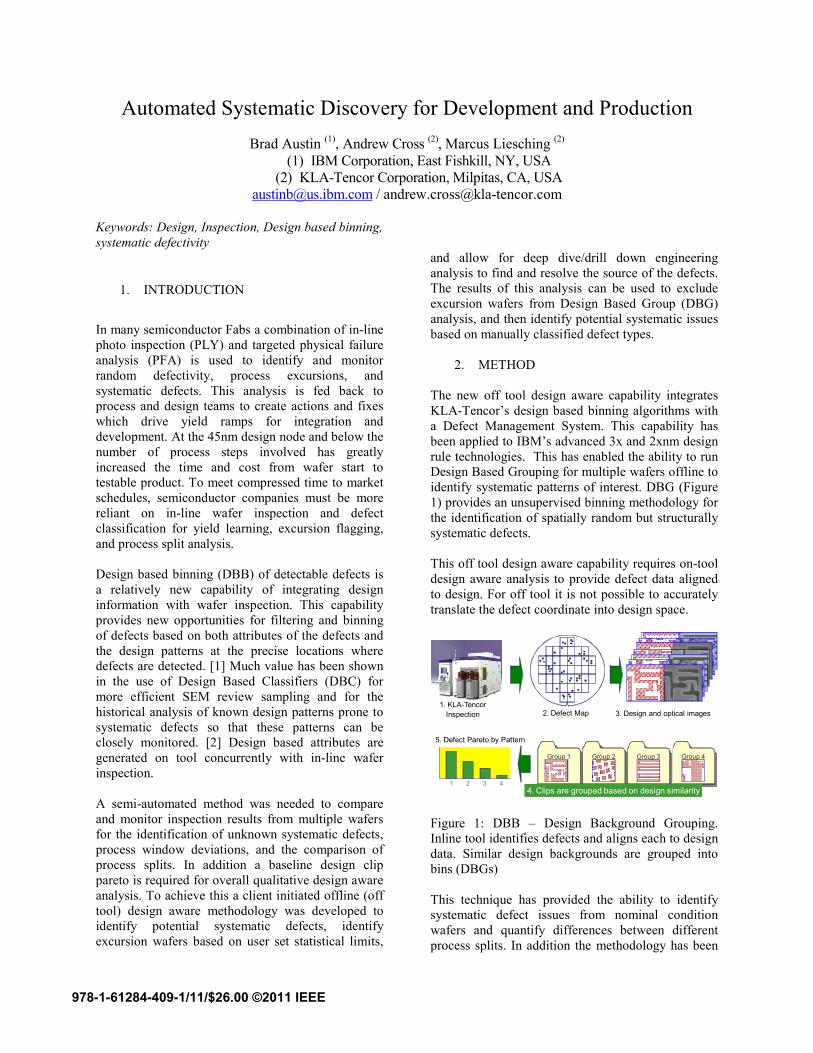
2. METHOD The new off tool design aware capability integrates KLA-Tencor’s design based binning algorithms with a Defect Management System. This capability has been applied to IBM’s advanced 3x and 2xnm design rule technologies. This has enabled the ability to run Design Based Grouping for multiple wafers offline to identify systematic patterns of interest. DBG (Figure 1) provides an unsupervised binning methodology for the identification of spatially random but structurally systematic defects. This off tool design aware capability requires on-tool design aware analysis to provide defect data aligned to design. For off tool it is not possible to accurately translate the defect coordinate into design space.
5. Defect Pareto by Pattern
1 2 3 4
1. KLA-TencorInspection 2. Defect Map 3. Design and optical images
Group 1 Group 2 Group 4Group 3
4. Clips are grouped based on design similarity Figure 1: DBB – Design Background Grouping. Inline tool identifies defects and aligns each to design data. Similar design backgrounds are grouped into bins (DBGs) This technique has provided the ability to identify systematic defect issues from nominal condition wafers and quantify differences between different process splits. In addition the methodology has been
978-1-61284-409-1/11/$26.00 ©2011 IEEE

applied to inline defectivity monitor data to enable automated identification of excursions of defects in specific DBG Bins for large data sets.
Figure 2: A Pareto of DBG bins for a set of scanned hardware. Design clips show similar pattern for selected bins. Each DBG bin contains a particular design region or pattern of interest where defectivity has been detected, and on the resultant pareto design clips can be shown for each bin (Example shown in Figure 2). DBG bins generally provide very high accuracy and purity for the design features they group. In addition Design Background Classification (DBC) can be utilized to investigate the historical impact of a particular systematic excursion. DBC allows supervised classification of known patterns of interest. When design background for a detected defect matches a previously defined design library, that defect is binned into the appropriate DBC bin (Figure 3).
Figure 3: DBB - Design Background Classification (DBC)
Figure 4: Historical tracking capability for DBC. DBC has been shown to be effective for identifying both historical and current excursions of potential systematic defect types of interest. Figure 4 shows a monitoring example where the defect count for a specific pattern of interest was monitored before and after an improvement was put in place. However given the comparative rarity of nominal wafer systematic excursions an automated excursion identification method was required. Figure 5 shows the excursion identification and control flow investigated. This methodology first allows the identification of systematic excursions on nominal wafers with the application of control limits on DBG bins. These control limits identify abnormal contributions to a specific bin from specific lots or wafers. In addition a control methodology for baseline identification of systematic issues related to DBG bins showing a difference to an expected value has been developed to identify baseline systematic issues. Because DBG bins are based on pattern matching and not area based, a nominal value based on defect density cannot be used. For this analysis the baseline for expected values is a random distribution of defects across the smallest repeating unit. In this case that is a single die. This is accomplished by populating an artificial die result with random distribution of defect coordinates. The DBB operation is executed in the same manner as a the true wafer results and thus a random defect pareto based on DBG bins is created and used as the basis for identification of systematic issues. DBG bins that vary greatly from the random distribution are considered systematic candidates.
3. KLA-TencorInspection 4. Defect Map 5. Design and optical images
ThinLine Dummy Location 1
Serp
1. Identify hot spots:OPC, DRC, FA, etc.
2. Build pattern library using design clips6. Defects are classified based on design
InspectionLocation mapping Design background
DBC library
DBC 1
DBC 2
DBC 3
DBC 4
DBC n
DBC 0
DBG binning
3. KLA-TencorInspection 4. Defect Map 5. Design and optical images
ThinLine Dummy Location 1
Serp
1. Identify hot spots:OPC, DRC, FA, etc.
2. Build pattern library using design clips6. Defects are classified based on design
InspectionLocation mapping Design background
DBC library
DBC 1
DBC 2
DBC 3
DBC 4
DBC n
DBC 0
DBG binning
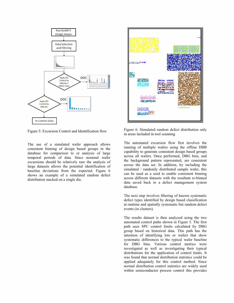
Figure 5: Excursion Control and Identification flow The use of a simulated wafer approach allows consistent binning of design based groups in the database for comparison to or analysis of large temporal periods of data. Since nominal wafer excursions should be relatively rare the analysis of large datasets allows the potential identification of baseline deviations from the expected. Figure 6 shows an example of a simulated random defect distribution stacked on a single die.
Figure 6: Simulated random defect distribution only in areas included in tool scanning The automated excursion flow first involves the running of multiple wafers using the offline DBB capability to generate consistent design based groups across all wafers. Once performed, DBG bins, and the background pattern represented, are consistent across the data set. In addition, by including the simulated / randomly distributed sample wafer, this can be used as a seed to enable consistent binning across different datasets with the resultant re-binned data saved back to a defect management system database. The next step involves filtering of known systematic defect types identified by design based classification at runtime and spatially systematic but random defect events (in clusters). The results dataset is then analyzed using the two automated control paths shown in Figure 5. The first path uses SPC control limits calculated by DBG group based on historical data. This path has the intention of identifying lots or wafers that show systematic differences to the typical wafer baseline for DBG bins. Various control metrics were investigated as well as investigating their typical distributions for the application of control limits. It was found that normal distribution statistics could be applied adequately for this control method. Since normal distribution control statistics are widely used within semiconductor process control this provides

the advantage of a well understood method to be utilized. Figure 7 shows an example of this excursion control path – identifying a potential excursion of a circular missing pattern affecting an SRAM cell.
Figure 7: Wafer / lot level DBG excursion identification example. This DBG bin on this wafer was flagged as out of control (OOC) The second control path makes use of the simulated random defectivity wafer to compare each DBG bin for the dataset under investigation to the expected defect percentage for each DBG bin. Figure 8 shows an example of such a comparison.
Figure 8: Comparison of actual DBG results to expected defect percentage. Show is a clip of a systematic missing pattern defect for an OCC DBG bin Where a specific DBG bin has a much greater percentage in defectivity compared with the expected value we can consider this a potential bin of interest for further investigation. With control limits based on this delta between the expected and actual results baseline systematic defect types that potentially affect multiple wafers / lots within a dataset can be
automatically identified. An example of such excursion identification can be seen in Figure 9 – showing a systematic bridging defect at gate level.
Figure 9: DBG type excursion identification In this case a systematically weak structure is identified which can now be monitored with a DBC library. This allows for sensitized control of the pattern type of interest. When a systematic pattern of interest is identified DBC can be run offline allowing an immediate quantification of the frequency of any pattern of interest occurring in historical data. This allows confirmation of whether a systematic event is a single temporal excursion or has been occurring at other intervals. Further, tool and process commonality or other deep dive analysis can be performed. Without this capability there would be a need to implement the design based classifier inline for data collection on future lots, requiring additional hardware be processed with this systematic issue before action could be taken. When comparing a split lot, where wafers from a common start and process history are processed under different conditions at a particular step, this control methodology can be used to identify specific systematic structures which are sensitive to the differing conditions so that they can be identified apart from structures which are common to both sides of the process split. Figure 10 shows an example where two wafers were processed using different design masks. Although the overall random defectivity for the two wafers was similar, two DBG bins stood out. Investigation into these pattern types revealed a systematic bridging defect which was very dense on only one of the design masks. Because of the automated nature of the control method, this type of important analysis can be performed immediately
Simulated wafer
Inspected wafers
Simulated wafer
Inspected wafers

after wafer scan is completed. Reducing the time required to evaluate experimental process or design changes.
Figure 8: Lot split comparison where sensitive DBG bins are identified This methodology is being investigated in the IBM East Fishkill facility to allow automated identification of potential systematic issues for critical devices.
3. CONCLUSIONS The general approach for systematic defect discovery has been with the use of modulated wafers investigating the litho process window. This approach is seen as essential for initial hot spot identification and process window qualification. However the ability to process multiple wafers and lots with consistent design based binning provides a significant enabler for systematic defect discovery and monitoring from nominal wafers; to identify process interactions that cannot be fully simulated using a single wafer and to identify any process or device induced hot spots over time. In addition the ability to consistently bin multiple wafers based on design allows the speedy comparison of process splits where patterns of interest can be identified as potential responses to different process conditions on different wafers. Overall this automated methodology will allow for faster identification of problems in line and lessen the time to implement corrective actions. References [1] Park A and Yeh, J. “Novel Technique to Identify Systematic and Random Defects during 65 nm and 45nm Process Development for Faster Yield Learning”. ASMC 2007. [2] Jansen, S. Florence, G. Perry, A Fox, S. “Utilizing Design Layout Information to Improve Efficiency of SEM Defect Review Sampling” ASMC 2008.
Patterns with new mask sensitivity
Patterns with old mask sensitivity