0+1+)-' functional materials by design for solar energ
TRANSCRIPT

Functional Materials by Design for Solar Energy Conversion
Bill Tumas
Associate Lab Director Materials and Chemical Science and Technology
National Renewable Energy Laboratory February 19, 2014
!""#$%&#"'(#)'*+)',"-)./'0+1+)-'

Director W. Tumas (NREL) Theory A. Zunger, Chief Scientist-Theory (CU)
S. Lany, P. Graf (NREL); V. Stevanovic (CSM) L. Yu, X. Zhang (CU), A.J. Freeman, G.Trimarchi (Northwestern)
Inorganic D.G. Ginley, Chief Scientist-Experiment (NREL) Synthesis J.D. Perkins, A Zakutayev, P. Ndione (NREL) & Characterization D.A. Keszler and J.F. Wager (Oregon State University);
K.R. Poeppelmeier and T.O. Mason (Northwestern University); M.Toney (SLAC)
Program Integrator L. Kazmerski, John Perkins
Acknowledgement: Center for Inverse Design EFRC
!"

Global Energy Challenge: Sustainable Materials, Processes and Systems
Cost ($/W) Performance
Reliability
Sustainable development is development that meets the needs of the present without compromising the ability of future generations to meet their own needs – UN Bruntland Commission
-! Greenhouse Gases -! Land Use -! Water Use -! Resources -! Hazards -! Waste
Integration at Scale

From Horse Power to Horsepower: The Great Horse-Manure Crisis of the 1890s
Shift Happens - Eric Morris, UC Davis

Solar Energy Generation AND
Storage/Use of Solar Energy
Materials ! Processes/Components ! Devices ! Systems
Thermal (heat)
Electrical (storage)
Fuels (chemical)
Solar (light)

Key Solar R&D Needs Addressed at NREL •! Applied R&D
•! Costs and efficiency, performance •! Understanding and control defects and interfaces •! Processing
•! Reliability -! Testing -! Prediction, Mechanisms of degradation
•! Manufacturing •! Next Generation
-! New absorbers/contacts -! Advanced processing -! New architectures, substrates, balance of system
•! Fundamental Research -! New materials by design -! Efficiency beyond the Shockley-Queisser limit -! Advanced manufacturing
Cost ($/W) Performance
Reliability

Gap between Cell and Module Efficiencies

Target Functionalities – Solar Energy Conversion
Solar Absorber Materials -! Strong solar absorption
Eg, absorptivity, SLME -! Carrier Lifetimes -! Carrier Diffusion recombination centers/defect -! Doping -! Low cost, non-toxic Transparent Conductors (n, p) - Transparency (band-structure) optical band gap > 3 eV - Conductivity (defects)
- Minimize hole-killer defects dopability, avoid formation of O-vacancies
- Maximize hole-producing defects intrinsic: vacancies, anti-sites, ... extrinsic: impurity doping
- Enhance hole mobility

• Semiconductor “high-tech” is based on just a handful of basic species: Si, Ge, GaAs, …
• These provide but a limited and sparse scale of band gaps:
Very ,Very few ….
0 1 2 3
InSb Ge Si InP GaAs AlAs eV
Some Observations

DOE Basic Research Needs Workshop report noted Missing Materials:
“ ! the range of materials currently available for use in photovoltaics is highly limited compared to the enormous number of semiconductor materials that can in principle be synthesized “ .
EERE invested in incremental refinement of the “usual-suspect materials” ( Si, CdTe, CIS !) Most involved accidental discoveries.
Need broad base of materials with optimized tailored properties not just few materials

11
Traditional approach: “Given a material, what are the properties” Inverse design: “Given a desired property, what is the material”
“Inverse Design”: Declare first the functionality you need, then use theory-guided experiment to iteratively find the material that has this target functionality
Center for Inverse Design

Center for Inverse Design
* tight coupling of theory and experiment * iterative attempts at a problem, teaching each other; * synergism between theory, synthesis and characterization
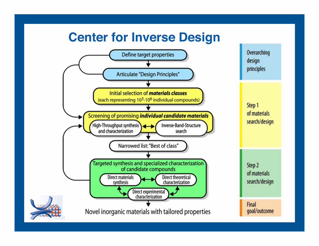
Center for Inverse Design!

Properties of interest •! Thermodynamic stability- !Hf •! Band structure and optical properties •! Defects and doping •! Carrier transport mechanism (band vs. small-polaron) •! !
Electronic structure methods •! Density functional theory
self-consistent charge density, total-energy •! Many body interactions in GW approximation
Quasi-particle energies, optical properties •! Credit to VASP group
Theory Tools
Tools for Inverse Design Tools for Inverse Design
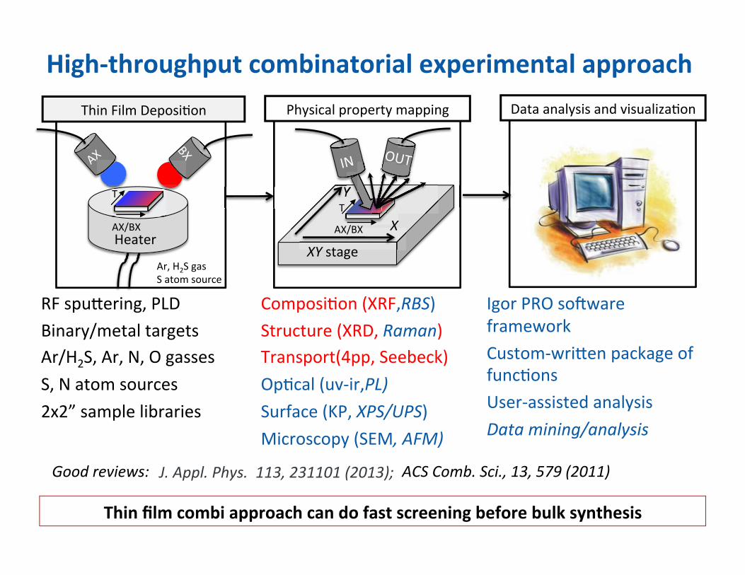
!"#$%&$'()#$*)&+,(-."/0&('"01+23*2'"-2/&01+0**'(0,$+
#$%&$'" 23"(&%)$"
3"
2"
*+",-.",-.,-.
3
./01"2034"5$67(0871"" 9/:(0;%3"6'76$'&:"4%6601)""
."
<=>?="
."
<=>?="
<'@"#!A")%("A"%&74"(7B';$"
5%&%"%1%3:(0("%1C"D0(B%30E%871"
F2"(6BG$'01)@"9H5"?01%':>4$&%3"&%')$&("<'>#!A@"<'@"+@",")%(($("A@"+"%&74"(7B';$("!I!J"(%463$"30K'%'0$("
L7467(0871"M=F2@456N"A&'B;&B'$"M=F5@"4%7%"N".'%1(67'&MO66@"A$$K$;PN",68;%3"MBDQ0'@89:"AB'R%;$"MS9@"286;<86N"T0;'7(;76:"MAUT='>0?:'
*)7'"9F,"(7VW%'$"R'%4$W7'P"LB(&74QW'0G$1"6%;P%)$"7R"RB1;871("-($'Q%((0(&$C"%1%3:(0("@%1%'7A"A".;%"%B/CAC'
4$"/+51-+,(-."+0**'(0,$+,0/+6(+708&+8,'22/"/#+.27('2+.)19+8:/&$28"8+
>D6'D#7EF'6GAF='HI='JKL'MNOHH:'PF'>QQBF'8R/CF''HHI='NIHHOH'MNOHI:S'T##U')-$A-VCW'
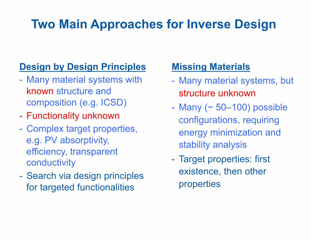
Two Main Approaches for Inverse Design
Design by Design Principles - Many material systems with
known structure and composition (e.g. ICSD)
- Functionality unknown - Complex target properties,
e.g. PV absorptivity, efficiency, transparent conductivity
- Search via design principles for targeted functionalities
Missing Materials - Many material systems, but
structure unknown - Many (~ 50–100) possible
configurations, requiring energy minimization and stability analysis
- Target properties: first existence, then other properties
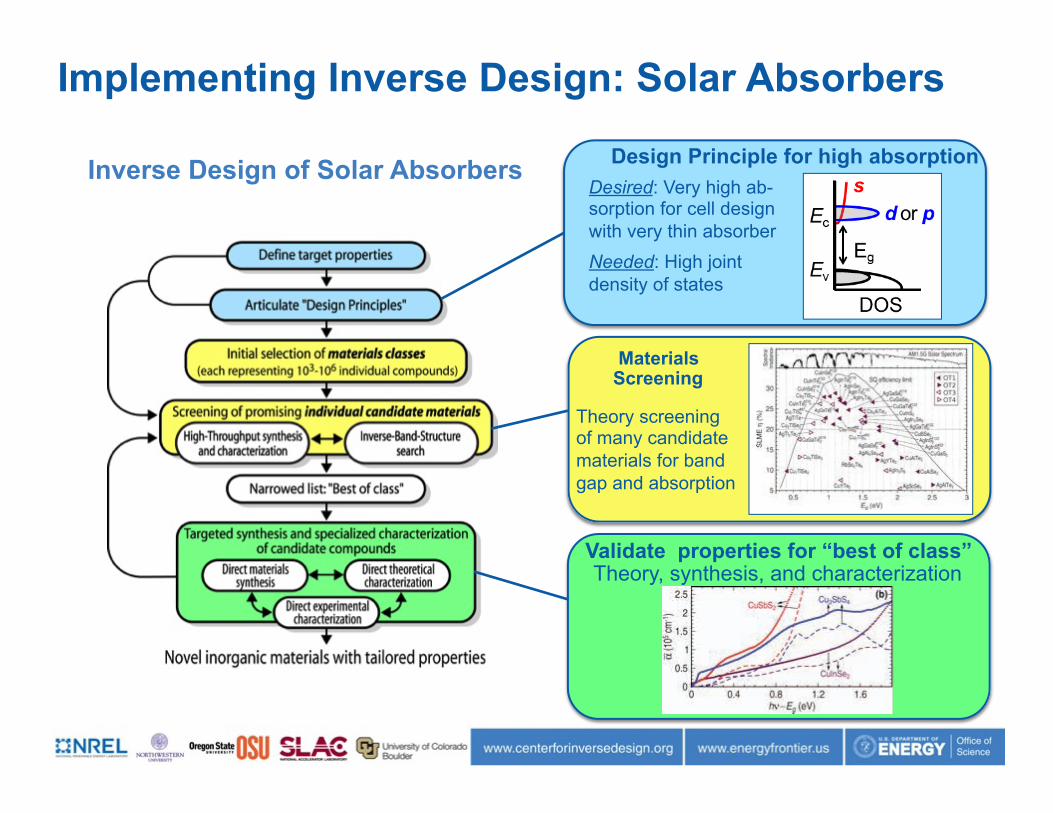
Inverse Design of Solar Absorbers Design Principle for high absorption
Validate properties for “best of class” Theory, synthesis, and characterization
Theory screening of many candidate materials for band gap and absorption
Materials Screening
Desired: Very high ab-sorption for cell design with very thin absorber Needed: High joint density of states
Implementing Inverse Design: Solar Absorbers
17

Inorganic Crystal Structure Database: ICSD
> 166,000 crystal structures; updated semi-annually http://www.fiz-karlsruhe.com/icsd.html

Selec<on Criteria: Spectroscopically Limited Maximum Efficiency-‐-‐SLME
• Detailed balance between cell inside and outside
• Photon energy dependent absorp8on
• Op8cal band gap type factor f(r) – non-‐radia8ve recombina8on
Captures physics of absorption, emission and recombination optical type, gaps and material-dependent non-radiative recombination loss
Yu, Zunger Phys Rev Lett 108, 068701 (2012)

Absorption Screening • High Throughput screening:
– First-principles quasi-particle GW method (G0W0+HSE06)
– Provides good band gap estimation
• Input: – ICSD structure – No element or stoichiometry
restrictions
• Output: – Band gap type – Absorption spectra – Electronic structure
20

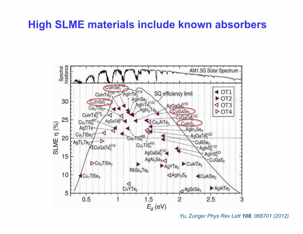
High SLME materials include known absorbers
Yu, Zunger Phys Rev Lett 108, 068701 (2012)

Other experimentally confirmed PV absorbers (less studied)
Yu, Zunger Phys Rev Lett 108, 068701 (2012)

Previously unrecognized high SLME materials
Yu, Zunger Phys Rev Lett 108, 068701 (2012)

In Cu-III-VI system: Cu3Tl1+Se2 has stronger absorption than CuTl3+Se2
In Cu3Tl1+Se2: -('2+41+*+"/+=CD+-('2+41+8+"/+EC+
Yu, Zunger Phys Rev Lett 108, 068701 (2012)

F$0&+,(/&'(18+&$2+8&'2/#&$+(7+(*<,01+0.8('*<(/G+
26 "! Increase p DOS near CBM and s DOS near VBM
4$2+6"'2,&+&'0/8"<(/+'0&2+HI2'-"J8+K(162/+'(12L>+
GaAs, CdTe
VB
CB
anion p
cation s
DOS
cation s VI s M p
Cu-M-VI
VI s
DOS
M p
VI p + Cu d M s
VI s VI s VI s M p M p
CuInSe2 (CIS)
Se p + Cu d
In s + Se s
In p In p
DOS
+ Cu d
In s + Se s
Se p +
In s + Se s
weak
Liping Yu

Cu-III-VI ! Cu-V-VI
=)%MMMH8N*OL%EM+ =)%EH8N*PL%EM+
<3"MXYN" 9"MZY@"XYN"
[%"MXYN" <("MZY@"XYN"
*1"MXYN" AK"MZY@"XYN"
.3"MXY@\YN" ?0"MZY@"XYN"
Low valence compound: Cu-V(3+)-VI High valence compound: Cu-V(5+)-VI
27

Case of Cu-Sb-S: Cu-Sb3+-S vs. Cu-Sb5+-S vs. CuInSe2 (CIS)
?7&/"LBXAKAX"%1C"LBAKA!"/%D$"(&'71)$'"%K(7'6871"&/%1"LBXAKAO"%1C"L*A"R7'"/]"^"U)Y_`"
_"C$6$1C("71"&/$"$1$'):"C0a$'$1;$"K$&W$$1"01C0'$;&")%6"%1C"C0'$;&")%6"LBAKA!"b""c`cZ"MU)U'd"U)A'N"""""LBXAKAXb"c`\X"MU)U'd"U)A'N"
3+='9F='-1'%BF'='!"#$%&'()*+%,-.()$%/0%1/%2345/6'
e<A9b""[cfcg#AUch"

Experiment shows same absorption trend in Cu-Sb-S case
By R. S Kokenyesi and D. A Keszler, Oregon State University
3+='9F='-1'%BF'='!"#$%&'()*+%,-.()$%/0%1/%2345/6'

More V p in Cu-V3+-VI compounds near CBM
VBM
CBM
CBM+2eV
VBM-2eV
CBM+2eV
VBM VBM
V p DOS
Ene
rgy
(eV
)
VBM-2eV VBM-2eV VBM-2eV
DOS
CBM
Integrated V p DOS near VBM
Inte
grat
ed V
p D
OS
near
CB
M
30

More V s in Cu-V3+-VI compounds near VBM
VBM
CBM
CBM+2eV
VBM-2eV
CBM+2eV
VBM VBM
V s DOS
Ene
rgy
(eV
)
VBM-2eV VBM-2eV VBM-2eV
DOS
CBM
Integrated V s DOS near VBM
Inte
grat
ed V
s D
OS
near
CB
M
31

Step 3: Experimental Realization
Low temperature synthesis Polycrystalline absorbers with rapid onset of absorption
(">105 cm-1 at EG+0.5 eV) Keszler et al. Oregon State
substrate Sb2S3
Cu
Sb2S3
substrate
polycrystalline Cu-V-VI
+S, 300°C

A;0$18i;"%66'7%;/"7R"&/$"jQ0*"6+R2S21(*-2/&J"6'7k$;&"
A3*1('0<(/" Q2820',$+ R2S21(*-2/&+
57W1Q($3$;871"R'74"4%1:"67((0K0308$(" R2S",28+@0&2'"018+
A3*1('0<(/ Q2820',$+ R2S21(*-2/&+R2S21(*-2/&+R2S21(*-2/&+R2S21(*-2/&+R2S21(*-2/&+
57W1Q($3$;871"R'74"4%1:"67((0K0308$(" R2S",28+@0&2'"018+ 57W1Q($3$;871"R'74"4%1:"67((0K0308$("
A&%&$"7R"&/$"%'&"'$($%';/"4$&/7C("2'74"4%&$'0%3("&7"C$D0;$("MX"(&$6(N"9'$C0;8D$"&/$7'$8;%3";%3;B3%871("#0)/Q&/'7B)/6B&";74K01%&7'0%3"$I6$'04$1&(""?'7%C"(;76$"7R"9e"4%&$'0%3(".$(&Q;%($(b"LBQA1QA"%1C"LBQAKQA"%K(7'K$'("+$I&Q)$1$'%871b"7I0C$QK%($C"%K(7'K$'("?'7%C3:"%6630;%K3$"&7"W0C$"'%1)$"7R"4%&$'0%3(""

Exploration of Cu-Sn-S family of materials
•! LBOA1AO"Q"&77"4%1:"/73$("M,/"LBN"•! LBOA1lA\h"Q"2$'40"3$D$3"MEFN"601101)"•! LB!A1AX"Q"R$W"/73$(@"17"U2"601101)"
=)N;/;P+"8+0+-('2+*'(-"8"/#+TE+0.8('.2'8+&$0/+(&$2'+=)%;/%;+-0&2'"018+
=)%;/%;+&$2('2<,01+*'26",<(/+
U+=)%;/%;+-0&2'"018+
Cu-Sn-S experimental realization
=)N;/;P+-0&2'"01+
=)%*(('+#'(V&$+
Zakutayev et al. Appl Phys Lett 103, 253902 (2013)'
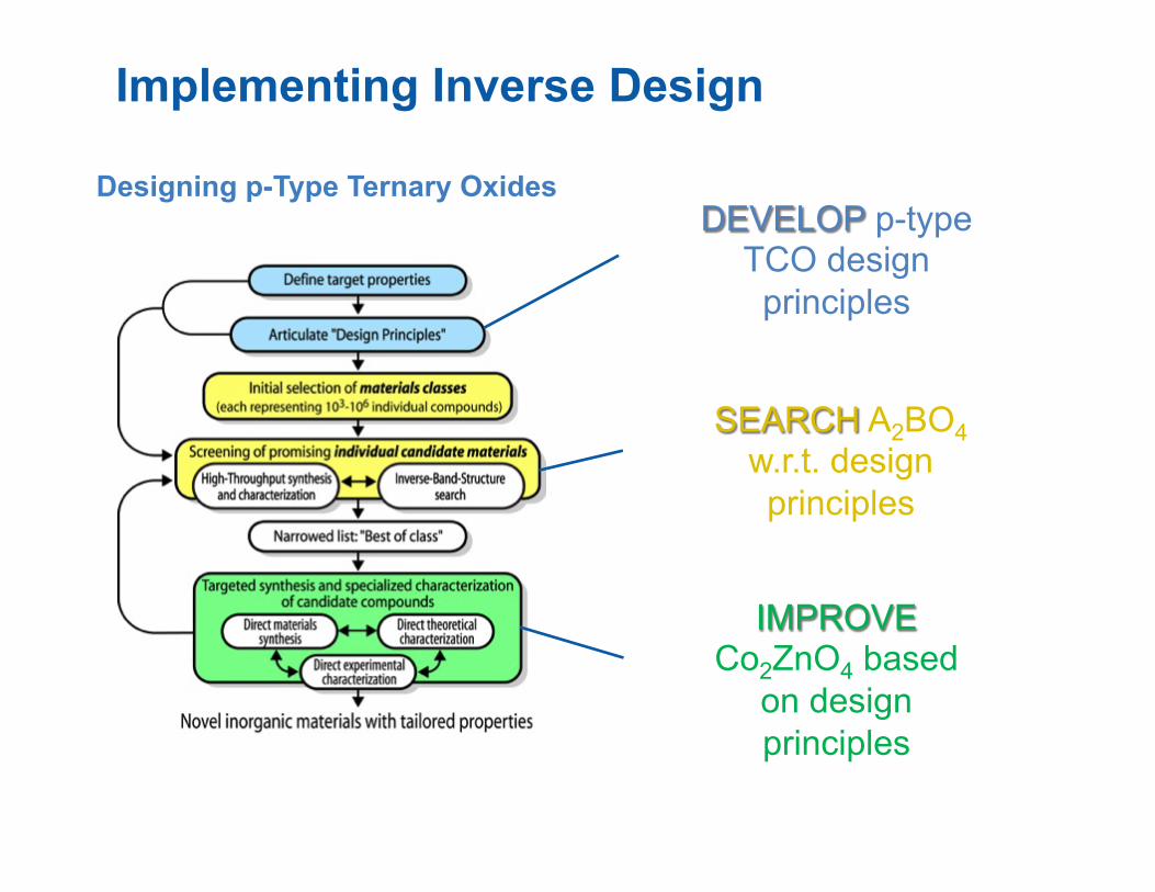
Designing p-Type Ternary Oxides
Implementing Inverse Design
DEVELOP p-type TCO design principles
SEARCH A2BO4 w.r.t. design principles
IMPROVE Co2ZnO4 based
on design principles

Modality 2 = Inverse Design By Design Principles
78*9%9:;(%<:'<('.)-=:'%2"(>(<.%<-;<$6%%
"""
78*9%9:;(%?:@8;8.+%2A:;-):'%<-;<$6%%
"
"
B)-'CA-)('<+%2@-'"DC.)E<.E)(%<-;<$6%
" ""
•!"<18QK71C01)"D%3$1;$"K%1C"4%I04B4"
•!"+7"K7B1C"673%'71("
•!"<K($1;$"7R"/73$QP033$'"C$R$;&"
•!"9'$($1;$"7R"/73$Q6'7CB;01)"C$R$;&("
•!",68;%3"K%1C")%6"^"X"$e"•!"f0C$"30)%1C"i$3C"(630m1)"M(74$";%($(N"
T%4=W+TQWTAQ4MA;+ RA;MKX+TQMX=MT?A;+
Chose Search Space: A2BO4 Spinels – 40 in ICSD
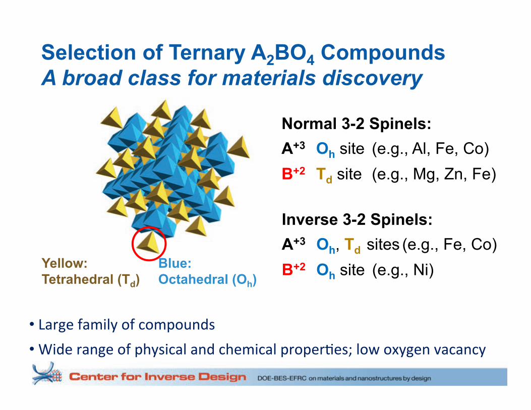
Normal 3-2 Spinels: A+3 Oh site (e.g., Al, Fe, Co) B+2 Td site (e.g., Mg, Zn, Fe)
Yellow: Tetrahedral (Td)
Blue: Octahedral (Oh)
•"H%')$"R%403:"7R";7467B1C(""•!"f0C$"'%1)$"7R"6/:(0;%3"%1C";/$40;%3"6'76$'8$(n"37W"7I:)$1"D%;%1;:"
Selection of Ternary A2BO4 Compounds A broad class for materials discovery
Inverse 3-2 Spinels: A+3 Oh, Td sites (e.g., Fe, Co) B+2 Oh site (e.g., Ni)

R(*"/#+Y+&:*28+
A3+ on Td is DONOR B2+ on Oh is ACCEPTOR
Paudel et al. Adv. Func. Matl 21, 4493 (2011) Perkins et al. Phys Rev B, 84, 205207 (2011)
Anti-site defects control properties:
DT-2--No Intrinsic Hole Killer !!
Co2(Zn,Ni)O4 – best of class!
Role of Anti-Site Defects in Spinels <K030&:"&7";%3;B3%&$"C$R$;&("%1C"C76%1&("0(";'08;%3"&7"$3$;&'710;"4%&$'0%3("C$(0)1"M(B6$';$33"%66'7%;/N"

12 of 40 A2BO4 Spinels Type 2 (Naturally P-Type)
VB
CB
Paudel et al, Advanced Functional Materials, 21, 01469 (2011)
Acceptor
Donor
Low Cost + Non-Toxic ! Take Co2ZnO4 as Prototype

Sputtered Co2ZnO4 Can Be Zn-Rich
Non-Equilibrium Theory - Excess Zn ! Oh Site - AXRD Confirms
Sputtered Films (TS = 340°C) - Zn-Rich Spinel Phase - Conductivity Increases
Annealed Films - Conductivity Decreases - Reduced Antisite Defects?
Perkins et al, Phys. Rev. B, 84, 205207 (2011)
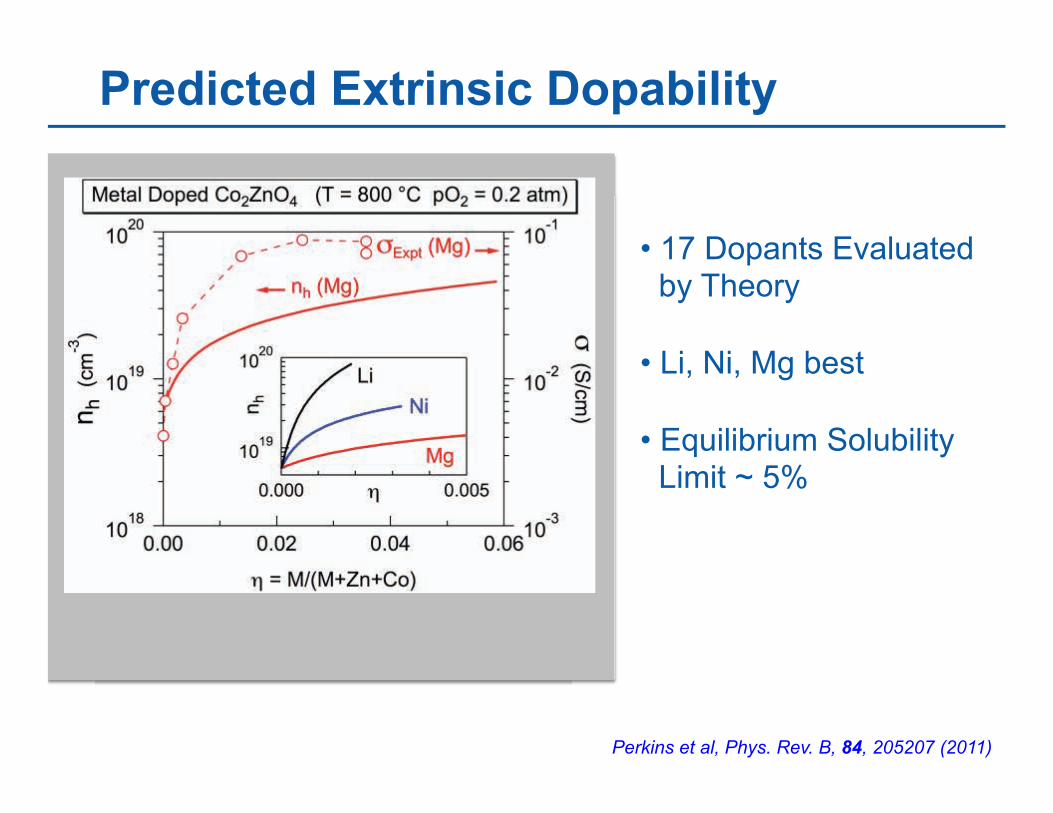
Predicted Extrinsic Dopability
• 17 Dopants Evaluated by Theory
• Li, Ni, Mg best • Equilibrium Solubility
Limit ~ 5%
Perkins et al, Phys. Rev. B, 84, 205207 (2011)
As shown in Fig. 1(a), the Zn–Ni–Co–O spinel thin filmsappear to have no other crystalline phases over a broad portionat the high-Co region of the ZnO–NiO–Co3O4 compositionrange; however, at low-Co regions rocksalt (NiO) and wurtzite(ZnO) phases are present. The color scale in Fig. 1(a) indicatesthe ratio of the sum of XRD intensities of ZnO (002) and NiO(111) peaks to the intensity of the spinel (311) peak. The com-positional range of stability for the spinel phase is broader (i.e.,the minimum amount of Co is lower) for Co3O4 co-doped withZn and Ni (Zn–Ni–Co–O) compared with Co3O4 doped withonly Zn (Zn–Co–O) or only Ni (Ni–Co–O). Within thespinel-only region, the XRD measurements cannot distinguishbetween a single-phase spinel solid solution and a multi-phasemixture of phase-separated spinels, because of the close matchof the lattice parameter of Co2ZnO4 (0.810 nm)[8] and Co2NiO4
(0.811 nm).[9] The stability range of the Zn–Ni–Co–O spinel
remains mostly unaffected by the 500 °C air anneal: onlyZn-rich films (<20 at.% Ni) show a 5–10 at.% decrease of thecomposition range of stability.
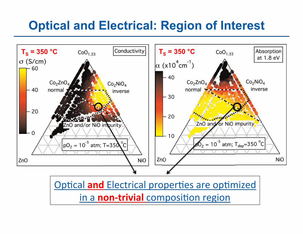
As shown in Fig. 1(b), co-doping of Co3O4 with Zn and Nidecreases the strength of the sub-gap absorption band at 689nm (1.8 eV), which is a relevant part of the spectrum for PVapplications. We attribute the sub-gap absorption α to opticaltransition between the Co atoms in tetrahedral (Td) and octa-hedral (Oh) coordination, because the absorption disappearsabove 33 at.% of Zn in Zn–Co–O (Co2ZnO4), at which Znatoms fill all available Td sites (1/3 of total cation sites), andabove 67 at.% of Ni in Ni–Co–O (CoNi2O4), at which Niatoms fill all available Oh sites (2/3 of total cation sites). Theabsence of absorption below the tie-line that connectsCo2ZnO4 and CoNi2O4 [dash-dotted line in Fig. 1(b)] suggeststhat the Zn–Ni–Co–O thin films are a mixture of Zn–Co–O
Figure 1. (Color online) (a) Crystalline phase purity and (b) optical absorption maps of Zn–Ni–Co–O thin films. The dashed and dash-dotted lines indicateCo2ZnO4–Co2NiO4 and Co2ZnO4–CoNi2O4 tie-lines, respectively. The dotted line indicates a phase boundary with NiO and ZnO. Symbols outlined by black lines in(a) show 44 points from one combinatorial library.
Figure 2. (Color online) (a) Conductivity σ of Zn–Ni–Co–O thin films. The dashed and dash-dotted lines indicate Co2ZnO4–Co2NiO4 and Co2ZnO4–CoNi2O4tie-lines, respectively. The dotted line indicates a phase boundary with NiO and ZnO impurity phases. (b) J–V curves and their parameters for PCDTBT:PCBMbulk heterojunction organic photovoltaic devices with amorphous hole transport layers with Zn1.65Co1.35O4 composition. The dashed line indicates a J–V curvemeasured in the dark.
2▪ MRS COMMUNICATIONS • www.mrs.org/mrc
As shown in Fig. 1(a), the Zn–Ni–Co–O spinel thin filmsappear to have no other crystalline phases over a broad portionat the high-Co region of the ZnO–NiO–Co3O4 compositionrange; however, at low-Co regions rocksalt (NiO) and wurtzite(ZnO) phases are present. The color scale in Fig. 1(a) indicatesthe ratio of the sum of XRD intensities of ZnO (002) and NiO(111) peaks to the intensity of the spinel (311) peak. The com-positional range of stability for the spinel phase is broader (i.e.,the minimum amount of Co is lower) for Co3O4 co-doped withZn and Ni (Zn–Ni–Co–O) compared with Co3O4 doped withonly Zn (Zn–Co–O) or only Ni (Ni–Co–O). Within thespinel-only region, the XRD measurements cannot distinguishbetween a single-phase spinel solid solution and a multi-phasemixture of phase-separated spinels, because of the close matchof the lattice parameter of Co2ZnO4 (0.810 nm)[8] and Co2NiO4
(0.811 nm).[9] The stability range of the Zn–Ni–Co–O spinel
remains mostly unaffected by the 500 °C air anneal: onlyZn-rich films (<20 at.% Ni) show a 5–10 at.% decrease of thecomposition range of stability.
As shown in Fig. 1(b), co-doping of Co3O4 with Zn and Nidecreases the strength of the sub-gap absorption band at 689nm (1.8 eV), which is a relevant part of the spectrum for PVapplications. We attribute the sub-gap absorption α to opticaltransition between the Co atoms in tetrahedral (Td) and octa-hedral (Oh) coordination, because the absorption disappearsabove 33 at.% of Zn in Zn–Co–O (Co2ZnO4), at which Znatoms fill all available Td sites (1/3 of total cation sites), andabove 67 at.% of Ni in Ni–Co–O (CoNi2O4), at which Niatoms fill all available Oh sites (2/3 of total cation sites). Theabsence of absorption below the tie-line that connectsCo2ZnO4 and CoNi2O4 [dash-dotted line in Fig. 1(b)] suggeststhat the Zn–Ni–Co–O thin films are a mixture of Zn–Co–O
Figure 1. (Color online) (a) Crystalline phase purity and (b) optical absorption maps of Zn–Ni–Co–O thin films. The dashed and dash-dotted lines indicateCo2ZnO4–Co2NiO4 and Co2ZnO4–CoNi2O4 tie-lines, respectively. The dotted line indicates a phase boundary with NiO and ZnO. Symbols outlined by black lines in(a) show 44 points from one combinatorial library.
Figure 2. (Color online) (a) Conductivity σ of Zn–Ni–Co–O thin films. The dashed and dash-dotted lines indicate Co2ZnO4–Co2NiO4 and Co2ZnO4–CoNi2O4tie-lines, respectively. The dotted line indicates a phase boundary with NiO and ZnO impurity phases. (b) J–V curves and their parameters for PCDTBT:PCBMbulk heterojunction organic photovoltaic devices with amorphous hole transport layers with Zn1.65Co1.35O4 composition. The dashed line indicates a J–V curvemeasured in the dark.
2▪ MRS COMMUNICATIONS • www.mrs.org/mrc
,68;%3"0/6"U3$;&'0;%3"6'76$'8$("%'$"76840E$C""01"%"/(/%&'"S"01+;7467(0871"'$)071"
Optical and Electrical: Region of Interest
TS = 350 °C TS = 350 °C

Three ways to improve conductivity in Co spinels
NZ+(/+W$+8"&2+*'(6),28+$(128 + +/(+$(12+9"112'8[+
\3+"-*'(S2-2/&+
1. Non-equilibrium growth
N]3+"-*'(S2-2/&+
2. Extrinsic dopants
O]]]]3+"-*'(S2-2/&+
3. Induce inverse spinel phase
@03"-"^2+&$"8+&(+"/,'2082+,(/6),<S"&:+


•!+X2V+-0&2'"018+0'2+1"921:+&(+$0S2+/2V+*'(*2'<28+
•!T'(*2'<28+$0S2+*'2S"()81:+.22/+23&'0,&26+"/+1"&2'0&)'2+7'(-+0/+"/,(-*12&2+82&+(7+-0&2'"018+H2_#_+M=;RL+
•!@0/:+$0S2+,01,)10&26+*'(*2'<28+7('+)/9/(V/+,(-*()/68+H2_#_+`Ca+$017%!2)812'+,(-*()/68L+.)&+$0S2/J&+62&2'-"/26+&$2"'+8&0."1"&:+H"_2_+23"8&2/,2L+
+•!=0/6"60&2+-0&2'"018+7('+011(:"/#+
@"88"/#+@0&2'"018+
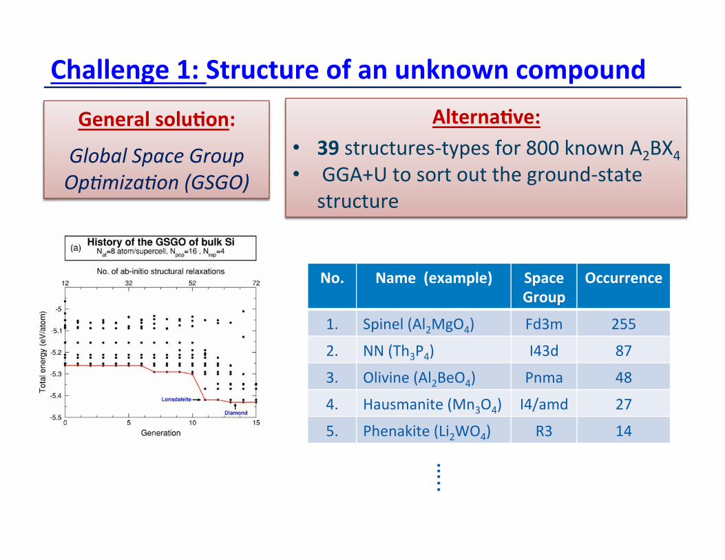
=$0112/#2+O>+;&'),&)'2+(7+0/+)/9/(V/+,(-*()/6+
K2/2'01+8(1)<(/>++
TB#E%B'6Q%G-'T)#+Q'*Q&7AY%&#"'MT6T*:'
`1&2'/0<S2>+•! Pb"(&'B;&B'$(Q&:6$("R7'"occ"P17W1"<!?=O"•! "[[<Y-"&7"(7'&"7B&"&/$")'7B1CQ(&%&$"(&'B;&B'$"
X(_+ X0-2++H230-*12L+ ;*0,2+K'()*+
W,,)''2/,2++
\`" A601$3"M<3!T),ON" 2CX4" !ZZ"
!`" ++"M./X9ON" *OXC" ol"
X`" ,30D01$"M<3!?$,ON" 914%" Oo"
O`" #%B(4%10&$"MT1X,ON" *O>%4C" !l"
Z`" 9/$1%P0&$"MH0!f,ON" FX" \O"
p``"

;(cV0'2+62S21(*-2/&>+
\N"A$m1)"B6"%B&74%8;%33:"&/$";':(&%3301$"%1C"4%)1$8;"(&'B;&B'$"R7'"$%;/"67&$18%3")'7B1C"(&%&$"
!N"<B&74%8;"C$&$;871"7R"$''7'(""
XN"<B&74%8;"$I&'%;871"7R"6'76$'8$("
!"#$+%+4$'()#$*)&+,01,)10<(/8+
;,(*2>+•! Och"<!?=O"•! Xq"(&'B;&B'$Q&:6$("R7'"$%;/"<!?=O"•! A$D$'%3"4%)1$8;";71i)B'%871("
de]+]]]+KK`Zf+;%3;B3%871("dO]g+=Tf$+B(01)"
Q26+@280+!T="

=$0112/#2+N>+;&0."1"&:+V"&$+'28*2,&+&(+,(-*2</#+*$0828+
_#RM<4?1=3N"r"U&7&M<4?1=3N""""d"""""M4sc<"Y"1sc?"Y"3sc=N"
.7&%3"$1$'):" U3$4$1&%3"'$R$'$1;$""$1$')0$("
!"<"Y"?"Y"O"="
`"`"`"
<!?=O" `"`"`"_#R"
<!=X"Y"?="
<?=X"Y"t"<!="Y"t"="

•! Fitted Elemental-phase Reference Energies (FERE) + GGA+U •! 50 µ0-values fit to 252 binary compounds with measured "Hf
=(''2,</#+RI4+7('+0,,)'0&2+h!7+Y+IAQA+

I"i26+A12-2/&01+Q272'2/,2+A/2'#"28+Y+IAQA++
Sn +0.18
Ge +0.15
Ga +0.66
Cd +0.35
Ca +0.29
Na +0.17
O +0.23
S +0.06
Se -0.07
Te -0.11
F +0.15
Cl +0.16
N -0.20
P -0.68
As -0.41
Sb -0.16
Bi -0.33
Si +0.43
Al +0.72
In +0.41
Zn +0.43
Hg +0.17
Cu +0.05
Ag -0.12
Ni +0.08
Co -0.10
Fe -0.15
Mn -0.03
Cr +0.07
V -0.45
Ti +0.05
Sc +0.49
Be +0.35
Mg
+0.55
Sr +0.51
Ba +0.54
Li +0.21
K +0.28
Rb +0.29
Au -1.26
Pd -0.27
Pt -0.43
Rh -0.53
Ir -0.19
La +0.20
Zr +0.72
Hf +0.72
Y +0.66
Nb +0.36
Ta +0.40
µ0 (FERE) = µ0 (GGA+U) + #µ0 (FERE)
cations anions
U=3 eV U=5 eV
Cu +0.05
Ag -0.12
Au
Zc"uc"D%3B$("iG$C"B(01)"4$%(B'$C"_#R"D%3B$("7R"!Z!"K01%':"610;8C$(@";/%3;7)$10C$("%1C"/%30C$("
V. Stevanovic, S. Lany, X. Zhang, and A. Zunger, Phys. Rev. B 85, 115104 (2012)

IAQA+E01"60<(/+%+42'/0'"28++
55 ternary compounds with measured "Hf
V. Stevanovic, S. Lany, X. Zhang, and A. Zunger, Phys. Rev. B 85, 115104 (2012)

A30-*12>+@/N;"Wj+
Theory: Structure: Olivine "Hf = -2.53 eV/atom
Experiment: Structure: Olivine "Hf = -2.56 eV/atom

How it Works: Mn2SiO4
Theory: Structure: Olivine "Hf = -2.53 eV/atom
Experiment: Structure: Olivine "Hf = -2.56 eV/atom

Example: Mn2SiO4
Theory: Structure: Olivine "Hf = -2.53 eV/atom
Experiment: Structure: Olivine "Hf = -2.56 eV/atom

Example: Mn2SiO4
-4.18 eV < "$O < -3.16 eV
Finch et al. J. Cryst. Growth, 29, 269 (1975)
T = 1600 K, pO2 = 10-10 atm
% "$O = -3.45 eV
Theory: Structure: Olivine "Hf = -2.53 eV/atom
Experiment: Structure: Olivine "Hf = -2.56 eV/atom

Example: Mn2SiO4, growth conditions
Theory: Structure: Olivine "Hf = -2.53 eV/atom
Experiment: Structure: Olivine "Hf = -2.56 eV/atom
Growth: T = 1600 K
pO2 = 10-10 atm
experiment
Mn : Si = 2 : 1

High-throughput Discovery of New A2BX4 Compounds
(A,B)
X
Rules: (1) only one transition metal at a time (2) respect possible oxidation states
Total 656 possible combinations 250 are reported 406 are not reported (“missing compounds”)
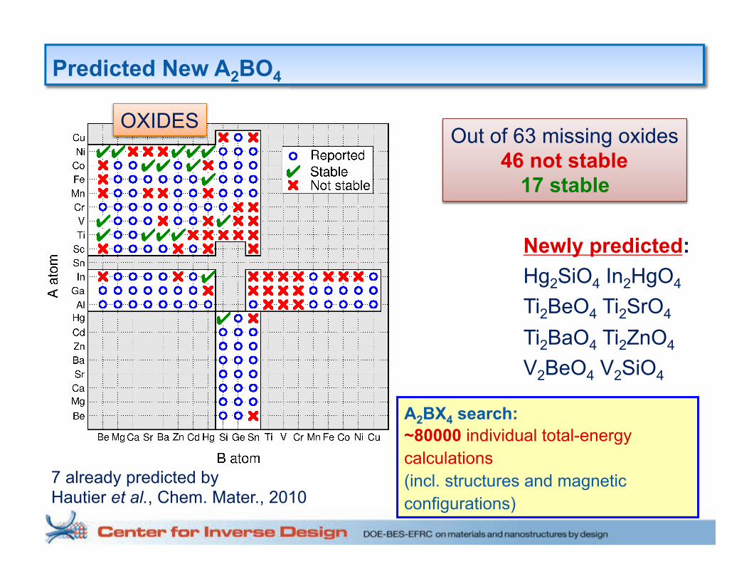
Predicted New A2BO4
Out of 63 missing oxides 46 not stable
17 stable
Newly predicted: Hg2SiO4 In2HgO4 Ti2BeO4 Ti2SrO4 Ti2BaO4 Ti2ZnO4 V2BeO4 V2SiO4
7 already predicted by Hautier et al., Chem. Mater., 2010
OXIDES
A2BX4 search: ~80000 individual total-energy calculations (incl. structures and magnetic configurations)

Results – Sulfides
We predict: Hg2GeS4, Al2TiS4, Al2VS4, Al2CoS4, Al2NiS4, In2VS4, Sc2BaS4, Ti2MgS4,!
Out of 92 not reported 34 stable,
1 undermined 57 not stable
Be"Mg"Ca"Sr"Ba"Zn"Cd"Hg"Al"Ga"In"Sn"Sc"Ti"V"Cr"Mn"Fe"Co"Ni"Cu"
Be"Mg"Ca"Sr"Ba"Zn"Cd"Hg"Si"Ge"Sn"Ti" V" Cr"Mn"Fe"Co"Ni"Cu"

CID Predicted Ternary Materials
!3FG1%?-.()8-;C%?-8'%*):EA%-'"%/"%(;(?('.CH%%IE.%:>%JK1%#-)8-=:'C0%13L%-)(%E')(A:).("%
544%A)("8<.("%C.-@;(0%55%E'"(.()?8'("0%-'"%/5K%A)("8<.("%':.%C.-@;(%
!FG%?-.()8-;C%M8.9%K%(;(<.):'CH%IE.%:>%N51%#-)8-=:'C0%1KK%-)(%E')(A:).("%
3/O%A)("8<.("%C.-@;(0%5K%E'"(.()?8'("0%-'"%3/O%A)("8<.("%':.%C.-@;(%%%
X. Zhang, V. Stevanovic, M. d'Avezac, S. Lany, and A. Zunger, Phys. Rev. B, 86, 014109 (2012)
X. Zhang et al., Adv. Funct. Mater. 22, 1425–1435 (2013).

30 compounds F-43m
15 compounds Pnma
6 compounds P21/c
2 compounds P63/mmc
2 compounds R-3m
1 compound P-3m1
1 compound P42/mmc 1 compound
Imm2
Identification of ABX ternary materials
a%'0:+6"k'0,<(/+"8+)8)011:+&$2+*'21"-"/0':+&((1+&(+"62/<7:+0+/2V+-0&2'"01_++`++708&+"62/<5,0<(/+(7+&$2+/2V+`Ca+,(-*()/68+"/+-)1<*$08",+80-*128+"8+*(88".12+.:+8"-)10</#+&$2+*0i2'/+(7+&$2+*'26",&26+8&'),&)'2_+
58 Stable and NOT reported ABX
18 electron compounds
The symmetry of a predicted stable
compound makes possible:
1) Simulation of diffraction pattern
2) Fast identification in the experimental
pattern

Fast identification in multiphasic sample
(110) zone
Simulation Experiment F-43m
Predicted crystal structure
&P-?A;(H%%!7M';.+QD1/?%
!7M';.D+l'Q$C"D+;,Q$42D+40=(;/D+40M'K2D+EM';"D+EQ$;"+0/6+!7Q$T+$0S2++
.22/+8$(V/+&(+,':8&011"^2+"/+&$2"'+
*'26",&26++,':8&01+8&'),&)'2_"
With Confirmation
By Electron diffraction
Identification of ABX ternary materials
The symmetry of a predicted stable
compound makes possible:
1) Simulation of diffraction pattern
2) Fast identification in the experimental
pattern
Single crystallite
X. Zhang et al. submitted to Nature Materials

Example: TaCoSn – A Semiconductor from 3 metals
Experiment: •!Thin film growth •! Potential absorber applications
Functionality of ABX ternary materials +
4$2('2<,01+,01,)10<(/8+(/+*'26",&26+H0/6+&$2/+8:/&$28"^26L+`Ca+-0&2'"018+*'(S"62+"/7('-0<(/+0.()&+&$2"'+*'(*2'<28_+
Indirect band gap of 1.3 eV Absorption onset at 1.6 eV High absorption above 1.8 eV
L%3;B3%&$C"5,A" L%3;B3%&$C"5,A"
>F'Z%[+1%/-$='-1'%BF='PF'>7F'DR-7F'6#GF'HIJ='HOO\]'MNOHI:''

Missing TaCoSn Compound
Not known in ICSD or ICDD Large stability range Predicted to have semi-conducting gap ~ 1.3 eV (GGA + U)

Validation: Growth of New TaCoSn
Predicted Structure
XRD: Predicted & Measured
TaCoSn Grown
>F'Z%[+1%/-$='-1'%BF='PF'>7F'DR-7F'6#GF'HIJ='HOO\]'MNOHI:''

M62/<5,0<(/+"/+-)1<*$08",+
80-*128+
I)/,<(/01"&:+
;&'),&)'2+62&2'-"/0<(/+
;&0."1"&:+
M/S2'82+R28"#/+G+M/S2'82+M/S2'82+M/S2'82+M/S2'82+M/S2'82+R28"#/+G+R28"#/+G+R28"#/+G+R28"#/+G+R28"#/+G+R28"#/+G+R28"#/+G+
Experiment
Experiment
Expe
rimen
t
Experiment
Inverse Design provides a scientific framework to accelerate the discovery of new materials

Summary
v"*1D$'($"5$(0)1""""""""""""""./$7':"""""""""""""""UI6$'04$1&"L7B6301)"0("L'08;%3"""""""""""""./$7':"%1C"UI6$'04$1&%3".773(""v""5$(0)1"D0%"5$(0)1"9'01;063$(""""""""""""A$3$;871";'0&$'0%"R7'"9e"%K(7'K$'(""""""""""""L7!w1,O"R'74"<!?=O"!"6Q&:6$".L,""""""""""""A$%';/"R7'"40((01)"4%&$'0%3("%1C"&/$0'"RB1;871%30&:"v"T%&$'0%3("5$(0)1"<66'7%;/"?'7%C3:"<6630;%K3$"""""""""""",&/$'"2B1;871%308$("v"T$&%(&%K030&:@"A:1&/$(0E%K030&:"""

cooperation and innovation “without borders” to develop and ready
emerging and revolutionary solar electricity
technologies toward the extended-time success of India’s Jawaharlal Nehru
National Solar Mission and the U.S. DOE SunShot
Program
Solar Energy Research Institute for India and US
SERIIUS
seriius.org

Research Thrusts Th
rust
s Sustainable Photovoltaics
(PV)
Multiscale Concentrated
Solar Power (CSP)
Solar Energy
Integration (SEI)
Act
iviti
es
Proj
ects
Core Projects
Ear
th A
bund
ant P
V
Adv
ance
d P
roce
ss/
Tech
nolo
gy
Mul
tisca
le M
odel
ing
and
Rel
iabi
lity
Hig
h-T,
Clo
sed-
Cyc
le,
Bra
vton
Cyc
le
Low
-T O
rgan
ic
Ran
kine
Cyc
le
Ther
mal
Sto
rage
&
Hyb
ridiz
atio
n
Roa
dmap
ping
, A
naly
sis
and
Ass
essm
ent
Grid
Inte
grat
ion
and
Ene
rgy
Sto
rage
Consortium Projects
• CONSORTIUM PROJECTS: disruptive, transformative R&D • CORE PROJECTS: core industry partner-led and focused
SERIIUS R&D Thrusts
Core Projects
Consortium Projects
Core Projects
Consortium Projects

Developing Low Cost Atmospheric Processing
Integration •! Materials/
devices integrated onto flexible substrates
Inks and synthesis •! Understanding
metalorganic decomposition
•! Molecular precursor design
•! Synthesis to desired materials
•! Inks: •! Absorbers •! Transparent
conductors •! Contacts/
Packaging
Deposition •! Desired
precursor with no residual organics
•! Designed to densify with and allow grain growth
•! Compatible with other layers
Processing •! Device quality:
•! Rapid thermal processing
•! Optical Processing

Acknowledgements: CID EFRC Partner Senior Inves<gators, Staff and Students, Graduates/Alumni
NREL Dave Ginley, John Perkins, Stephan Lany, Andriy Zakutayev, Peter Graf, Jun Wei Luo, Paul Ndione, Haowei Peng, Vince Bollinger, Josh Mar&n, Mayeul d’Avezac, Alberto Franceschem, Arkadiy Mikhaylushkin
Northwestern University
Ken Poeppelmeier, Art Freeman, Tom Mason, Giancarlo Trimarchi, Feng Yan, Arpun Nagaraja, Jimo Im, Kanber Lam, Romain Gau&er, Kelvin Chang, Jeremy Harris, Karl Rickers, Evan Stampler, Nicola Perry, Veerle Cloet, Adam Raw
Oregon State University
Doug Keszler, John Wager, Robert Kokenyesi, Jae-‐Seok Heo, Greg Angelos, Brian Pelae, Ram Ravichandran, Jeremy Anderson, Vorranutch Jieratum, Ben Waters, Emmeline Altschul
University of Colorado -‐ Boulder
Alex Zunger, Liping Yu, Lijun Zhang, Josh Ford
SLAC Mike Toney, Linda Lim, Kevin Stone, Yezhou Shi, Joanna Bemnger
Colorado School of Mines
Vladan Stevanovic, Xiuwen Zhang

Summary
v"*1D$'($"5$(0)1""""""""""""""./$7':"""""""""""""""UI6$'04$1&"L7B6301)"0("L'08;%3"""""""""""""./$7':"%1C"UI6$'04$1&%3".773(""v""5$(0)1"D0%"5$(0)1"9'01;063$(""""""""""""A$3$;871";'0&$'0%"R7'"9e"%K(7'K$'(""""""""""""L7!w1,O"R'74"<!?=O"!"6Q&:6$".L,""""""""""""A$%';/"R7'"40((01)"4%&$'0%3("%1C"&/$0'"RB1;871%30&:"v"T%&$'0%3("5$(0)1"<66'7%;/"?'7%C3:"<6630;%K3$"""""""""""",&/$'"2B1;871%308$("v"T$&%(&%K030&:@"A:1&/$(0E%K030&:"""

Acknowledgements: CID EFRC Partner Senior Inves<gators, Staff and Students, Graduates/Alumni
NREL Dave Ginley, John Perkins, Stephan Lany, Andriy Zakutayev, Peter Graf, Jun Wei Luo, Paul Ndione, Haowei Peng, Vince Bollinger, Josh Mar&n, Mayeul d’Avezac, Alberto Franceschem, Arkadiy Mikhaylushkin
Northwestern University
Ken Poeppelmeier, Art Freeman, Tom Mason, Giancarlo Trimarchi, Feng Yan, Arpun Nagaraja, Jimo Im, Kanber Lam, Romain Gau&er, Kelvin Chang, Jeremy Harris, Karl Rickers, Evan Stampler, Nicola Perry, Veerle Cloet, Adam Raw
Oregon State University
Doug Keszler, John Wager, Robert Kokenyesi, Jae-‐Seok Heo, Greg Angelos, Brian Pelae, Ram Ravichandran, Jeremy Anderson, Vorranutch Jieratum, Ben Waters, Emmeline Altschul
University of Colorado -‐ Boulder
Alex Zunger, Liping Yu, Lijun Zhang, Josh Ford
SLAC Mike Toney, Linda Lim, Kevin Stone, Yezhou Shi, Joanna Bemnger
Colorado School of Mines
Vladan Stevanovic, Xiuwen Zhang