01 cover - diagramas dediagramasde.com/diagramas/otros/sony_dvp-ns325_ns330_ns333_ns430... ·...
TRANSCRIPT

DVP-NS325/NS330/NS333/NS430/NS433/NS530/NS725P/NS730P
4-5 4-6
AF-098 BOARD MB-108 BOARD
IC102 ed1
2.5Vp-p
H
IC102 ea2
2.0Vp-p
H
IC102 wl3
2.0Vp-pH
IC102 wf4
2.0Vp-p
H
IC102 ws5
1.4Vp-p
H
IC102 w;6
1.4Vp-p
H
IC404 37
3.9Vp-p
125nsec
IC103 31
3.3Vp-p
1.17msec
IC103 82
3.3Vp-p
38nsec
IC103 9 q;3
3.3Vp-p
42nsec
IC103 qg4
IC104 tf5
3.3Vp-p
60nsec
IC201 2 (CD PB)6
20nsec
IC201 2 (DVD PLAY)6
0.79Vp-p
20nsec
IC201 ra (CD PB)7
1.6Vp-p
IC201 ra (DVD PLAY)7
1.7Vp-p
IC201 rs (CD PB)8
383mVp-p
IC201 rs (DVD PLAY)8
433mVp-p
IC201 tl9
1.3Vp-p
890nsec
IC301 (DVD PLAY)10
1.34Vp-p40ns/div
IC301 (CD PB)11
1.46Vp-p
0.2us/div
IC301 (CD PB)12
1.5Vp-p
1.8msec
IC301 (DVD PLAY)12
1.62Vp-p
1.0msec
IC301 (CD PB)13
770mVp-p
21msec
IC301 (DVD PLAY)13
466mVp-p
32.4msec
IC30114
1.1Vp-p
30nsec
IC403 ws15
3.3Vp-p
40nsec
IC403 tg16
1.0Vp-p
63.5usec
IC403 tj17
979mVp-p
63.5usec
IC403 tl18
675mVp-p
63.5usec
IC403 ya19
666mVp-p
6.35usec
IC403 yd20
625mVp-p
6.8usec
IC403 yg21
1.1Vp-p
33.5usec
IC40322
3.3Vp-p
38nsec
IC502 r;23
3.3Vp-p
36nsec
IC50224
3.3Vp-p
18.3nsec
IC504 es25
3.3Vp-p
36nsec
IC504 ej26
483mVp-p
63.5nsec
IC504 ek27
633mVp-p
63.5usec
IC504 el28
131Vp-p
63.5usec
IC504 rs29
508Vp-p
280nsec
IC504 rd30
979mVp-p
63.5usec
IC504 rf31
1.08Vp-p
63.4usec
IC601 132
3.3Vp-p
42nsec
3.3Vp-p
30nsec
0.47Vp-p
111
125
125
150 158
103
160
113
124
124
WAVEFORMSAF-098/MB-108

DVP-NS325/NS330/NS333/NS430/NS433/NS530/NS725P/NS730P
1
A
B
C
D
E
F
G
H
I
J
2 12 1311109876543 14 15
4-9 4-10
For Schematic Diagram• Refer to page 4-7 for printed wiring board of AF-98 board.• Refer to page 4-5 for waveform• Refer to page 4-17 for Differential Part List
The components identified bymark or dotted line with mark
are critical for safety.Replace only with partnumber specified.
Les composants identifiés parune marque sont critiquespour la sécurité. Ne lesremplacer que par une pièceportant le numéro spécifié.
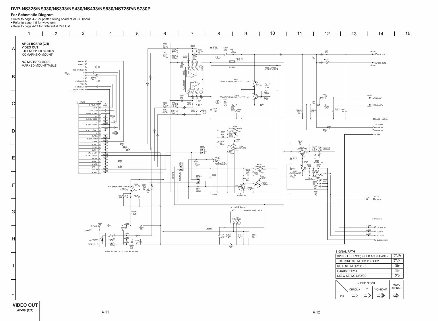
AF-98 BOARD (1/4)AUDIO OUT-REF.NO.:1000 SERIES-XX MARK:NO MOUNT
NO MARK:PB MODEMARKED:MOUNT TABLE
0.1
-5.0
0.03
0.01
0
0.2
5.0
0.03
-5.0
-5.0
0.2
0.01
0.04
0
0.2
5.0
0
00
0
0.4
0.6
0
0.6
3.5
0.4
1.2
0
0.1
0.4
1.2
0
0.6
3.5
0.6
-5.0
-13.
1
0 -5.0
-5.0
0.1
3.4
0.03
5.0
5.00.03
0.3
0
0
0.06
5.0
0.1
3.4
0.1
0.1
1
2
5
6
3
4
1 TO (2/2)
TO MB108 BOARD ( )CN
1000V100p
120u200V
18mH
47u35V
MTZJ7.5MA4075
0.0022u50V
0.0001u50V
2200p250v
0.022u50V
0.1u250V
SIGNAL PATH
VIDEO SIGNAL
CHROMA
PB
Y Y/CHROMA
AUDIOSIGNAL
AUDIO OUTAF-98 (1/4)
DVP-NS325/NS330/NS333/NS430/NS433/NS530/NS725P/NS730P
1
A
B
C
D
E
F
G
H
I
J
2 12 1311109876543 14 15
4-11 4-12
For Schematic Diagram• Refer to page 4-7 for printed wiring board of AF-98 board.• Refer to page 4-5 for waveform• Refer to page 4-17 for Differential Part List
AF-98 BOARD (2/4)VIDEO OUT-REF.NO.:2000 SERIES-XX MARK:NO MOUNT
NO MARK:PB MODEMARKED:MOUNT TABLE
-13.
3
1.3
1.3 0
10.8
01.3
1.3
1.72
2.4
1.7
5.0
5.0
0
5.0
0 10.3
0
-13.10
0
0
-13.1
-13.1
10.2
10.2
10.2
0.1
0
0.1
0
3.2
4.8 3.4
0.1
0.1
10.2
0.03
0.03
0.1
0
14.0
14.0
-14.0
-15.0
-15.2
10.0
11.011.0
1
2
3
4
5
6
7
8
9
10
11
12
13
14
15
16
17
18
19
20
21
22
23
24
25
1000.25W
2.2k0.25W 2.55k
0.25W
68010V
47010V
1k0.25W
1/16W10k
2250V
xx 4725V
2700.5W1000
10V1/4W1.5k
10025V 2.7k
0.25W
2SC3311A-QTA
1500.5W
0.5W
25d965-QTA
10k0.25W
SB290
10k0.25WFE1D
SB290 xx
680.25W
33025V
10010V
xx
1.8k0.25W
25D965-QTA
UF4007-AMMO
681W
10025V
S1230705
VIDEO SIGNAL
CHROMA
PB
Y Y/CHROMA
AUDIOSIGNAL
SIGNAL PATH
SPINDLE SERVO (SPEED AND PHASE)
TRACKING SERVO DVD/CD CDV
SLED SERVO DVD/CD
FOCUS SERVO
SKEW SERVO DVD/CD
VIDEO OUTAF-98 (2/4)

DVP-NS325/NS330/NS333/NS430/NS433/NS530/NS725P/NS730P
1
A
B
C
D
E
F
G
H
I
J
2 12 1311109876543 14 15
4-13 4-14
For Schematic Diagram• Refer to page 4-7 for printed wiring board of AF-98 board.• Refer to page 4-5 for waveform• Refer to page 4-17 for Differential Part List
AF-98 BOARD (3/4)PS TROUGH-REF.NO.:4000 SERIES-XX MARK:NO MOUNT
NO MARK:PB MODEMARKED:MOUNT TABLE
3.5
2.0
0
3.5
0.3
3.2
-14.5
-15.2 -15.2
0
5.0
1.3
3.5
5.0
PS TROUGHAF-98 (3/4)

DVP-NS325/NS330/NS333/NS430/NS433/NS530/NS725P/NS730P
1
A
B
C
D
E
F
G
H
I
J
2 12 1311109876543 14 15
4-15 4-16
For Schematic Diagram• Refer to page 4-7 for printed wiring board of AF-98 board.• Refer to page 4-5 for waveform• Refer to page 4-17 for Differential Part List
AF-98 BOARD (4/4)IF-REF.NO.:4000 SERIES-XX MARK:NO MOUNT
NO MARK:PB MODEMARKED:MOUNT TABLE
0
4.0
4.0
-10.1
-13.0
-15.3
-14.3-13.0
-6.0
-10.2
0
0
1.1
1.5
0
4.0
0
3.4
4.0
0
4.0
4.0
0
0
3.1
2.0
3.4
3.4
0
0
0
0
0
3.5
3.5
0 4.0
4.0
0 4.0
2.7
0 0 0 4.0
4.0
4.0
4.0
0 4.0
-15.
3
-6.4
-6.3
-6.5
-6.4
-6.4
-15.2
-12.4
-15.2
-15.2
-12.4
-7.1
-4.3
-15.2
-12.4
-15.2
-7.0
-7.0
-4.3
-7.0
7.0
2.0
-15.2
-12.4
-15.2
-4.3
-7.0
-15.
2
-15.
2
-15.
2
15.2
13.0
13.0
13.0
13.0
13.0
13.0
13.04.000
7
NS725/NS730
NS725/NS730
Except NS725/NS730
IFAF-098 (4/4)

DVP-NS325/NS330/NS333/NS430/NS433/NS530/NS725P/NS730P
4-17 4-18
NS325 NS330/NS333 NS430/NS433 NS530 NS725P NS730P
C212 xx 1u 1u xx xx xx50V 50V
C215 xx 220p 220p 220p xx 220p50V 50V 50V 50VCH CH CH CH
C216 xx 220p 220p 220p xx 220p50V 50V 50V 50VCH CH CH CH
C227 xx xx 47u 47u 47u 47u16V 16V 16V 16V
D203 xx DAP202K-T- DAP202K-T- xx xx xx871991445 871991445
IC204 xx xx GP1FA55OTZ GP1FA55OTZ GP1FA55OTZ GP1FA55OTZ874901731 874901731 874901731 874901731
Q206 xx MUN2213T1 MUN2213T1 xx xx xx872902489 872902489
Q209 xx UN2217-TX UN2217-TX xx xx xx872942472 872942472
Q210 xx MSB709-RT1 MSB709-RT1 xx xx xx872901005 872901005
R214 xx 4700 4700 xx xx xx
R231 xx 10k 10k xx xx xx
R232 xx 10k 10k xx xx xx
R233 xx 47k 47k xx xx xx
R235 4700 xx xx 4700 4700 4700
R236 xx 10k 10k xx xx xx
R237 xx 4700 4700 xx xx xx
R239 xx 100k 100k xx xx xx
R242 xx xx xx xx xx xx
R243 xx xx xx xx xx xx
[AUDIO]
NS325/NS330/ NS725P/NS730NS333/NS430/NS433/NS530
CN402 7p 7p177063811 177063811
CN406 xx xx
D401 xx EB3804X-TP650017601
R436 xx 10k
R437 10k xx
R461 xx 220
[IF]
AF-98 Board Differential Part List
[VIDEO]
NS325/NS530 NS330/NS333/ NS730P/NS430/NS433 NS725P
C112 0.1u xx 0.1u16V 16VB B
CN102 xx 21P xx181514911
D108 HZM6.8WA1 xx HZM6.8WA1871907115 871907115
D109 HZM6.8WA1 xx HZM6.8WA1871907115 871907115
IC102 LA73050-TL LA73051-TL LA73053-TL875985645 875982646 670182001
J102 3P xx 3P179344511 179344511
J103 179419811 xx 179419811
Q104 MUN2213T1 xx MUN2213T1872902489 872902489
Q105 MUN2111T1 xx MUN2111T1872902483 872902483
Q106 xx 2SA1162-YG xx872923047
R121 10K xx 3300
R122 xx 1K xx
R127 68 xx 68
R128 68 xx 68
R129 10K xx 10K
R133 68 xx 68

DVP-NS325/NS330/NS333/NS430/NS433/NS530/NS725P/NS730P
1
A
B
C
D
E
F
G
H
I
J
2 12 1311109876543 14 15
4-21 4-22
For Schematic Diagram• Refer to page 4-19 for printed wiring board of ER-21 board.
ER-21 BOARD (NS330: AE1,AE2,UK,RUS/NS333/NS430/NS730P)EURO AV-REF.NO.:9000 SERIES-XX MARK:NO MOUNT
NO MARK:PB MODEMARKED:MOUNT TABLE
B- B-
B-
B+
B+
B+ B+
B+
B+
1.1 4.7
-0.6
3.4
3.4
-0.6
3.4
-0.6
-0.1
3.4
-5.1
-5.1
11.7
4.9
11.7
11.7
4.9
3.4
0
0
0
0
0.5
0.5
0.6
0.5
0
0
0
0
3.3
0.1
LINE(RGB)-TV
IC 901
VIDEO BUFFER
EURO AVER-21

DVP-NS325/NS330/NS333/NS430/NS433/NS530/NS725P/NS730P
1
A
B
C
D
E
F
G
H
I
J
2 12 1311109876543 14 15
4-25 4-26
SYSTEM CONTROLMB-108 (1/6)
For Schematic Diagram• Refer to page 4-23 for printed wiring board of MB-108 board.• Refer to page 4-5 for waveform• Refer to page 4-37 for Differential Part List
The components identified bymark or dotted line with mark
are critical for safety.Replace only with partnumber specified.
Les composants identifiés parune marque sont critiquespour la sécurité. Ne lesremplacer que par une pièceportant le numéro spécifié.
MB-108 BOARD (1/6)SYSTEM CONTROL-REF.NO.:1000 SERIES-XX MARK:NO MOUNT
NO MARK:REC/PB MODE
1
23
4
5

DVP-NS325/NS330/NS333/NS430/NS433/NS530/NS725P/NS730P
1
A
B
C
D
E
F
G
H
I
J
2 12 1311109876543 14 15
4-27 4-28
MOTOR DRIVEMB-108 (2/6)
2.0
2.0
2.0
2.0
2.0
2.0
0
2.0
2.0
2.0
2.0
2.0
2.0
2.0
2.0
0.01
3.4
3.4
0 0 3.4
3.4
3.4
3.4
11.0
5.3
5.3
-0.05
6.0
5.0
5.3
5.3
5.4
5.2
-0.05
5.3
5.3
5.3
0
5.3
11.05.3
3.4
2.0
2.0
2.0
5.0
2.4
3.2
3.2
2.0 0
3.2
3.2
0
2.0
0
3.3
0.03
0.03
2.4
0.03
0.030.022.50.03
0.03
3.0
0.1
5.0
5.0
0 3.0
0.1
0
0.1
0 4.4
3.1
2.1
0.1
2.1
2.2
3.0
0.04
3.0
0.3
1.3
2.2
0.05
2.0
3.0
2.0
2.0
4.0
0.4
4.0
0.04
0.1
0
3.4
1.0
3.2
3.00
2.2
2.2
3.2
3.2
2.3
3.0
5.0
4.0
4.0
4.0
4.0
4.0
3.0 3.2 5.1
1.05.1
6
7
8
9
MS-81
For Schematic Diagram• Refer to page 4-23 for printed wiring board of MB-108 board.• Refer to page 4-5 for waveform• Refer to page 4-37 for Differential Part List
MB-108 BOARD (2/6)MOTOR DRIVE-REF.NO.:2000 SERIES-XX MARK:NO MOUNT
NO MARK:PB MODE
VIDEO SIGNAL
CHROMA
PB
Y Y/CHROMA
AUDIOSIGNAL
SIGNAL PATH
SPINDLE SERVO (SPEED AND PHASE)
TRACKING SERVO DVD/CD CDV
SLED SERVO DVD/CD
FOCUS SERVO
SKEW SERVO DVD/CD

DVP-NS325/NS330/NS333/NS430/NS433/NS530/NS725P/NS730P
1
A
B
C
D
E
F
G
H
I
J
2 12 1311109876543 14 15
4-29 4-30
SERVOMB-108 (3/6)
For Schematic Diagram• Refer to page 4-23 for printed wiring board of MB-108 board.• Refer to page 4-5 for waveform• Refer to page 4-37 for Differential Part List
MB-108 BOARD (3/6)SERVO-REF.NO.:3000 SERIES-XX MARK:NO MOUNT
NO MARK:PB MODE
0
0
0.1
0
1.2
0
2.0
1.0
1.0
3.0
3.4
3.4
0
0
2.0
0
0
0
3.4
2.0
0
2.0
0
3.1
2.0
3.4
3.4
3.4
3.2
3.1
2.0
2.0
0.1
3.2
3.2
3.1
3.2
3.2
3.4
3.1
3.0
3.1
2.4
3.0
0
3.2
3.2
3.1
3.2
3.1
3.2
3.2
2.0
3.4
2.0
2.0
3.4
3.00
3.4
3.4
3.0
3.4
0.3
0.1
0.3
0.2
0.4
0.5
0.3
0.2
0.2
0.20
2.0
1.3
3.000
2.0
3.0
2.0
0.5
2.0
2.00
2.0
3.1
0
2.0
1.0
2.4
3.3
0
2.0
2.0
2.0
-0.03
2.0
2.0
3.3
-0.04
0.5
0
3.3
0
1.0
0
3.4
3.0
2.0
3.3
2.0
0
1.0
0
3.4
0
3.4
0
0
0
0
2.0
2.0
0
2.0
2.2
0
0
1.0
0
3.4
2.0
2.1
1.4
1.1
1.4
1.0
1.0
2.0
3.4
2.0
0 0 2.0
0.1
0 2.0
2.0
0 1.5
0 3.4
3.4
0 0 3.4
3.4
3.0
3.4
3.4
3.4
0 3.3
0 0 0 2.0
3.4
3.0
2.0
0 1.3
1.7
2.0
3.4
3.3
3.0
3.2
3.3
3.4
3.2
3.2
3.2
4.0
0
0
0
3.1
3.3
0
0
0.2
0.2
0.3
0.2
4.0
0.2
0.2
0.3
0.1
0.2
0.2
0
0
3.3
3.3
0
0
3.1
3.2
3.1
3.1
0
3.2
3.2
3.2
3.2
0
5.0 5.0
0
1.3 3.3
10
11
1213
14
VIDEO SIGNAL
CHROMA
PB
Y Y/CHROMA
AUDIOSIGNAL
SIGNAL PATH
SPINDLE SERVO (SPEED AND PHASE)
TRACKING SERVO DVD/CD CDV
SLED SERVO DVD/CD
FOCUS SERVO
SKEW SERVO DVD/CD

DVP-NS325/NS330/NS333/NS430/NS433/NS530/NS725P/NS730P
1
A
B
C
D
E
F
G
H
I
J
2 12 1311109876543 14 15
4-31 4-32
AV DECODERMB-108 (4/6)
For Schematic Diagram• Refer to page 4-23 for printed wiring board of MB-108 board.• Refer to page 4-5 for waveform• Refer to page 4-37 for Differential Part List
MB-108 BOARD (4/6)AV DECODER-REF.NO.:4000 SERIES-XX MARK:NO MOUNT
NO MARK:PB MODE
0
2.1
3.4
5.0
3.1
0
3.2
5.0
0
1.3
03.4
1.1
2.0
2.0
2.2
3.4
2.1
2.0
0
2.0
2.0
3.4
0.1
0.1
1.4
3.4
0.1
0.1
0.1
2.0
2.4
1.5
1.5
0
2.0
2.0
0
2.0
2.0
3.4
2.0
2.0
0
1.2
1.5
3.4
0.1
1.3
3.0
3.0
3.1
2.0
0.1
0.1
0.5
2.0
0.12
3.4
03.4
1.0
2.0
0
2.1
2.4
3.4
2.0
2.0
0
2.0
2.0
3.4
0.1
1.4
0.1
3.4
-0.05
0.1
0.1
2.0
1.2
1.5
1.5
0
2.0
2.0
0
2.0
1.4
3.4
2.0
1.5
0
1.0
2.0
3.4
0.1
3.1
3.0
3.0
3.1
1.0
0.1
0.1
1.0
2.0
1.0
3.4
0
0
0
4.33.4
0
2.1
2.2
3.4
2.0
1.0
0
1.0
1.0
0.5
2.1
3.4
2.0
1.1
1.0
1.1
1.3
1.0
1.2
2.3
1.3
0
0.1
0.1
0
3.3
3.0
0
0
0
3.0
3.4
4.0
3.3
3.3
2.0
0
0.03
0
0.3
0.04
4.0
0.1
2.4
0.3
3.0
0
3.3
1.0
1.3
0
1.0
1.0
1.4
1.2
0
2.0
1.0
1.0
1.3
2.0
2.0
2.0
2.0
0
0
2.0
1.0
1.0
2.0
0
2.0
2.0
0
0
0
3.4
2.0
2.0
2.0
2.0
0
0
2.0
2.0
3.4
3.4
0
0
3.4
3.4
0
0
0
3.4
2.0
2.0
4.0
4.0
3.4
3.4
0.1
0.1
2.1
2.0
2.0
2.0
1.1
1.0 0
1.0 0 0
2.0
0.5
1.2 0 0
2.0
3.4
1.2
2.1
2.0
2.0
3.2
3.4
3.4
3.1
3.4
3.40
3.4
3.4
3.4
3.4
1.0
1.0
0.2 0
2.0
2.1 0
2.4
1.0
3.4
3.4
4.0 0 0 0 0
2.0
2.0
2.0 0
3.3
0.3
0 0.3
3.3
1.0
0 1.0
3.3
2.0
0 0.3
0 3.4
2.0
3.3
0.4
0.4
4.0
2.0
3.2
0 0 0 2.0
0 0 0 4.0
4.0
0 2.0
1.0
1.2
2.0
2.0
2.0
1.1
1.1
3.0
2.0
3.1
0 2.0
3.1
0 3.3
3.0
0 0 0
16 17 1918 20 21
15
22
SIGNAL PATH
VIDEO SIGNAL
CHROMA
PB
Y Y/CHROMA
AUDIOSIGNAL

DVP-NS325/NS330/NS333/NS430/NS433/NS530/NS725P/NS730P
1
A
B
C
D
E
F
G
H
I
J
2 12 1311109876543 14 15
4-33 4-34
I/P CONVERTERMB-108 (5/6)
For Schematic Diagram• Refer to page 4-23 for printed wiring board of MB-108 board.• Refer to page 4-5 for waveform• Refer to page 4-37 for Differential Part List
MB-108 BOARD (5/6)1/P CONVERTER-REF.NO.:5000 SERIES-XX MARK:NO MOUNT
NO MARK:PB MODE
23
24
25
26
27
29
28
3031
SIGNAL PATH
VIDEO SIGNAL
CHROMA
PB
Y Y/CHROMA
AUDIOSIGNAL

DVP-NS325/NS330/NS333/NS430/NS433/NS530/NS725P/NS730P
1
A
B
C
D
E
F
G
H
I
J
2 12 1311109876543 14 15
4-35 4-36
AUDIO DAC, PLLMB-108 (6/6)
For Schematic Diagram• Refer to page 4-23 for printed wiring board of MB-108 board.• Refer to page 4-5 for waveform• Refer to page 4-37 for Differential Part List
MB-108 BOARD (6/6)AUDIO DAC, PLL-REF.NO.:6000 SERIES-XX MARK:NO MOUNT
NO MARK:PB MODE
0
3.4
3.4
3.4
2.0
1.2
2.0
2.0
5.0
5.0
5.0
0
2.4
2.4
2.4
2.4
1
TO AF-98 BOARD CN203 (PAGE )

DVP-NS325/NS330/NS333/NS430/NS433/NS530/NS725P/NS730P
4-37 4-38
MB-108 Borad Differential Part List
NS325 NS330 NS333/NS430/ NS725P NS730PNS530
C401 10u 10u 10u xx xx16V 16V 16V
C403 0.01u 0.01u 0.01u xx xx25V 25V 25VB B B
C405 100u 100u 100u xx xx6.3V 6.3V 6.3V
C420 0.1u 0.1u 0.1u xx xx16V 16V 16VB B B
IC402 TK11133CSC TK11133CSC TK11133CSC xx xx670230201 670230201 68230201
IC403 CXD1935Q CXD1935Q CXD1935Q CXD1935Q CXD1935Q875241960 875241960 875241960 875241645 875241645
R401 0 0 0 xx xx
R403 470 470 470 xx xx
R406 220 220 220 xx xx
R407 220 220 220 xx xx
R408 220 220 220 xx xx
R409 220 220 220 xx xx
R410 220 220 220 xx xx
R411 220 220 220 xx xx
R415 xx xx xx 10 10
R436 xx xx xx 0 0
R438 xx xx xx 0 0
R439 0 0 0 0 0
RV401 1k 1k 1k xx xx122358341 122358341 122358341
[MB-108 (4/6)]
NS325 NS330 NS333/NS430/ NS725P NS730PNS433/NS530
FB602 146978421 146978421 146978421 xx xx
FB603 146978421 146978421 146978421 xx xx
R607 0 0 0 xx xx
R608 0 0 0 xx xx
R609 0 0 0 xx xx
R612 0 0 0 xx xx
R613 xx xx xx 0 0
R614 xx xx xx 0 0
[MB-108 (6/6) AUDIO]
NS325 NS330 NS333/NS430/ NS725P NS730PNS433/NS530
P5 xx xx xx Mount Mount
[MB-108 (5/6) I/P CONVERTER]
NS325 NS330/NS333 NS530 NS725P NS730PNS430/NS433
C441 xx 0.01u 0.01u 0.01u 0.01u25V 25V 25V 25VB B B B
C442 xx 0.01u 0.01u 0.01u 0.01u25V 25V 25V 25VB B B B
C447 xx 0.01u 0.01u 0.01u 0.01u25V 25V 25V 25VB B B B
IC404 GLT5160L16 GLT5160L16 GLT5160L16 GLT5160L16 GLT5160L16670384201 670384201 670384201 670384201 670384201
IC405 xx GLT5160L16 GLT5160L16 GLT5160L16 GLT5160L16670384201 670384201 670384201 670384201
[MB-108 (4/6) AV DECODER]
NS325 NS330 NS333/NS430/ NS725P NS730PNS433/NS530
C106 9p 9p 9p 9p 12p50V 50V 50V 50V 50VCH CH CH CH CH
C107 10p 10p 10p 10p 12p50V 50V 50V 50V 50VCH CH CH CH CH
C124 xx xx xx xx xx
C130 xx 0.01u 0.01u xx 0.01u25v 25v 25vB B B
CN101 9P 9P 9P 9P 9P181633921 181633921 181633921 181633921 181633921
R164 xx 22k 12k 12k 4700
R166 xx xx xx 47k 22k
R169 xx 12k 47k 47k 6800
IC101 CAT24WC16J CAT24WC16J CAT24WC16J CAT24WC16J CAT24WC16J875956153 875956153 875956153 875956153 875956153
IC104 MB91307RPF MB91307RPF MB91307RPF MB91307RPF MB91307RPF670183701 670305901 670305901 670305901 670305901
IC108 xx IDT71V016S IDT71V016S xx IDT71V016S670187401 670187401 670187401
[MB-108 (1/6)]
DVP-NS325/NS330/NS333/NS430/NS433/NS530/NS725P/NS730P
1
A
B
C
D
E
F
G
H
I
J
2 12 1311109876543 14 15
4-41 4-42
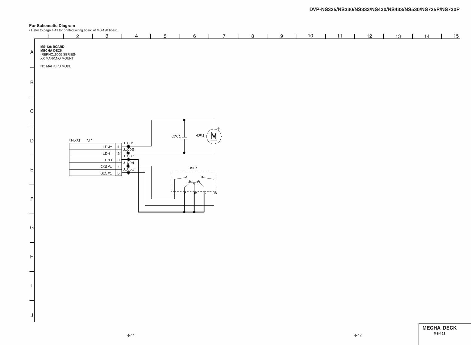
For Schematic Diagram• Refer to page 4-41 for printed wiring board of MS-128 board.
MS-128 BOARDMECHA DECK-REF.NO.:6000 SERIES-XX MARK:NO MOUNT
NO MARK:PB MODE
MECHA DECKMS-128

DVP-NS325/NS330/NS333/NS430/NS433/NS530/NS725P/NS730P
1
A
B
C
D
E
F
G
H
I
J
2 12 1311109876543 14 15
4-45 4-46
For Schematic Diagram• Refer to page 4-45 for printed wiring board of SW-384 board.
The components identified bymark or dotted line with mark
are critical for safety.Replace only with partnumber specified.
Les composants identifiés parune marque sont critiquespour la sécurité. Ne lesremplacer que par une pièceportant le numéro spécifié.
SW-384 BOARDSWITCH-REF.NO.:1000 SERIES-XX MARK:NO MOUNT
NO MARK:REC/PB MODE
Except NS430/NS433/NS725P/NS730P
Except NS430/NS433/NS725P/NS730P
NS430/NS433/NS725P/NS730P NS725P/NS730P
NS325/NS333/NS430/NS433/NS530/NS725P/NS730P
NS430/NS433/NS725P/NS730P X
X
XX
SWITCHSW-384
SW-384 Borad Differential Part List
NS325/NS330/ NS430/NS433 NS725/NS730NS530
JS801 121629591 xx xx
JS811 xx 121629591 121629591
R812 xx xx 3900
S801 176219621 xx xx
S802 176219621 xx xx
S805 176219621 xx xx
S811 xx xx 176219621
S812 xx 176219621 176219621
S814 xx 176219621 176219621
S815 xx 176219621 176219621

DVP-NS325/NS330/NS333/NS430/NS433/NS530/NS725P/NS730P
1
A
B
C
D
E
F
G
H
I
J
2 12 1311109876543 14 15
4-49 4-50
For Schematic Diagram• Refer to page 4-49 for printed wiring board of HS8S2U board.
The components identified bymark or dotted line with mark
are critical for safety.Replace only with partnumber specified.
Les composants identifiés parune marque sont critiquespour la sécurité. Ne lesremplacer que par une pièceportant le numéro spécifié.
SWITCHING REGULATORPOWER BLOCK (HS8S2U)
HS8S2U BOARDSWITCHING REGULATOR-REF.NO.:1000 SERIES-XX MARK:NO MOUNT
NO MARK:REC/PB MODE

DVP-NS325/NS330/NS333/NS430/NS433/NS530/NS725P/NS730P
1
A
B
C
D
E
F
G
H
I
J
2 12 1311109876543 14 15
4-53 4-54
For Schematic Diagram• Refer to page 4-53 for printed wiring board of ETXNY410E0F board.
ETXNY410E0F BOARDSW REG-REF.NO.:3000 SERIES-XX MARK:NO MOUNT
NO MARK:PB MODE
SW REGPOWER BLOCK (ETXNY410E0F)

DVP-NS325/NS330/NS333/NS430/NS433/NS530/NS725P/NS730P
1
A
B
C
D
E
F
G
H
I
J
2 12 1311109876543 14 15
4-57 4-58
For Schematic Diagram• Refer to page 4-57 for printed wiring board of ETXNY410M0F board.
ETXNY410M0F BOARDSW REG-REF.NO.:5000 SERIES-XX MARK:NO MOUNT
NO MARK:PB MODE
SW REGPOWER BLOCK (ETXNY410M0F)

6-1
6-3. SYSCON DIAGNOSIS
The same contents as board detail check by serial interface canbe checked from the remote commander. On the Test Mode Menuscreen, press - key on the remote commander, and thefollowing check menu will be displayed.
### Syscon Diagnosis ###Check Menu
0. Quit1. All2. Version3. Peripheral4. Servo5. Supply6. AV Decoder7. Video8. Audio_
0. QuitQuit the Syscon Diagnosis and return to the Test Mode Menu.
1. (All items continuous check)This menu checks all diagnostic items continuously. Normally,all items are checked successively one after anotherautomatically unless an error is found, but at a certain item thatrequires judgment through a visual check to the result, thefollowing screen is displayed for the key entry.
### Syscon Diagnosis ###
Diag All CheckNo. 2 Version
2-3. ROM Check SumCheck Sum = 2005
Press NEXT Key to ContinuePress PREV Key to Repeat_
For the ROM Check, the check sum calculated by the Syscon isoutput, and therefore you must compare it with the specifiedvalue for confirmation.Following the message, press > key to go to the next item,or . key to repeat the same check again.
6-1. GENERAL DESCRIPTION
The Test Mode allows you to make diagnosis and adjustmenteasily using the remote commander and monitor TV. Theinstructions, diagnostic results, etc. are given on the on-screendisplay (OSD).
6-2. STARTING TEST MODE
Press the [TOP MENU], [CLEAR], [POWER] keys on theremote commander in this order with the power of main unit inOFF status, and the Test Mode starts, then “DIAG START” willbe displayed on the fluorescent display tube and the menushown below will be displayed on the TV screen. At the bottomof menu screen, the model name and revision number aredisplayed. Last Off at the lower right of screen indicates theinformation code concerning the last power off. To execute eachfunction, select the desired menu and press its number on theremote commander. To exit from the Test Mode, press the [I/ ]key.
Test Mode Menu
0. Syscon Diagnosis1. Drive Auto Adjustment2. Drive Manual Operation3. Mecha Aging4. Emargency Hisory5. Version Information6. Video Level Adjustment
Exit: Power Key_Model : DPX-17xxxxRevision : x.xxx Last Off: xx
Power Off Information Code List00 : Primary Power Off01 : Power Off Request from SYSTEM CONTROL02 : Power Off by Emergency Power Off Command from
SYSTEM CONTROL(if information is sent from SYSTEM CONTROL)
03 : IF CON Judged that SYSTEM CONTROL is Faulty04 : Power Off from Diagnosis Mode of IF CON05 : Forced Power Off by the User06 : Power Off by Power Supply Voltage Monitor
SECTION 6TEST MODE
DVP-NS325/NS330/NS333/NS430/NS433/NS530/NS725P/NS730P
1

6-2
*In "All item continuous check", pressing step or enter will notquit the diagrosis.
Selecting 2 and subsequent items calls the submenu screen ofeach item. When “–––––” is displayed in the submenu, it meansthat the test is not supported in the model.
For example, if “5. Supply” is selected, the following submenuwill be displayed.
### Syscon Diagnosis ###Check MenuNo. 5 Supply
0. Quit1. All2. ARP Register Check3. ARP to RAM Data Bus4. ARP to RAM Address Bus5. ARP RAM Check_
0. QuitQuit the submenu and return to the main menu.
1. (All submenu items continuous check.)This menu checks 2 and subsequent items successively. At theitem where visual check is required for judgment or an erroroccurred, the checking is suspended and the message is outputfor key entry. Normally, all items are checked successively oneafter another automatically unless an error is found.Selecting 2 and subsequent items executes respective menusand outputs the results.For the contents of each submenu, see “General Description ofChecking Method” and “Check Items List”.
General Description of Checking Method2. Version(2-2) Revision
ROM revision number is displayed.Error: Not detected.The revision number defined in the source file isdisplayed with four digits.
(2-3) ROM Check SumCheck sum is calculated.Error: Not detected.8-bit data are added up to the ROM address 0x000F0000to 0x002EFFFF, and the result is displayed with 4-digithexadecimal number. Error is not detected. Compare theresult with the specified value.
(2-4) Model TypeModel code is displayed.Error: Not detected.The model code read from the EEPROM is displayedwith 2-digit hexadecimal number.
(2-5) RegionRegion code is displayed.Error: Not detected.The region code determined from the model code isdisplayed.
(2-6) M’t checkMount resistance is checked.Error 22: The region code does not accord.Check wether the region code that is deduced from modelresistance and destination resistance accords with theregion code that is deduced from region resistance value.
3. Peripheral(3-2) EEPROM Check
Data write t read, and accord checkError 03: EEPROM write/read discord0x9249, 0x2942 and 0x4294 are written to the address0x00 to 0xFF of the EEPROM and then read forchecking. Before writing, the data are saved, then afterchecking, they are written to restore the contents ofEEPROM.
(3-6) Venc Check (NS755V/NS915V)Data write t read, and accord checkError 52: Write and read data discord.Accessing to the SYSCON may be defective.
(3-8) External RAM CheckTest Data write t read, and accord checkError 02: The external RAM used in the system control ischecked.
To quit the diagnosis and return to the Check Menu screen,press x or [ENTER] key. If an error occurred, the diagnosis issuspended and the error code is displayed as shown below.
### Syscon Diagnosis ###
3-3. EEPROM CheckError 03: EEPROM Write/Read NAddress : 00000001Write Data : 2492Read Data : 2490Press NEXT Key to ContinuePress PREV Key to Repeat_
Press x key to quit the diagnosis, or . key to repeat thesame item where an error occurred, or > key to continue thecheck from the item next to faulty item.

6-3
4. Servo(4-2) Servo DSP Check
Data write t read, and accord checkError 12: Read data discord0x9249, 0x2942 and 0x4294 are written to the RAMaddress 0x602 of the Servo DSP and then read forchecking.
(4-3) ––––––––––Check no support.
(4-4) RF Amp Register CheckDate write t read, and accord checkError 13: RF Amp resister write, and read data discordImplement 8-bit shift operation of the 0x01 to thereadable/writable register of the RF Amp. If once writedata do not accord with read data, it is NG.
5. Data Supply System(5-2) ARP Register Check
Data write t read, and accord checkError 08: ARP register write, and read data discordData 0x00 to 0xFF is written sequentially to the ARPTMAX register (address 0xC6) and then read forchecking.
(5-3) ARP to RAM Data BusData write t read, and accord checkError 09: ARP Tt RAM data bus errorData 0x0001 to 0x8000 where one bit each is set to 1 arewritten to the address 0 of RAM (IC303) connected to theARP (IC302) through the bus, then they are read andchecked. In case of discord, written bit pattern and readdata are displayed. If data where multiple bits are 1 areread, the bits concerned may touch each other. Further, ifdata where certain bit is always 1 or 0 regardless ofwritten data, the line could be disconnected or shorted.
(5-4) ARP to RAM Address BusData write t other address read discord checkError 10: ARP Tt RAM address bus errorCaution: Address and data display in case of an error is
different from the display of other diagnosis(described later).
Before starting the test, all addresses of RAM (IC303) arecleared to 0x0000.First, 0xA55A is written to the address 0x00000, and theaddress data are read and checked from addresses0x00001 to 0x80000 while shifting 1 bit each. Next, thedata at that address is cleared, and it is written to theaddress 0x00001, and read and checked in the samemanner. This check is repeated up to the address 0x80000while shifting the address data by 1 bit each.If data other than 0 is read at the addresses except writtenaddress, an error is given because all addresses werealready cleared to 0. In this check, the error displaypattern is different from that of other diagnosis; read data,written address, and read address are displayed in thisorder. However, the message uses same template, andaccordingly exchange Address and Data when reading.The following display, for example,
### Syscon Diagnosis ###
5-4. ARP to RAM Address BusError 10: ARP - RAM Address BAddress : 0000A55AWrite Data : 00000000Read Data : 00080000Press NEXT Key to ContinuePress PREV Key to Repeat_
shows the data 0xA55A was read from address0x00080000 though it was written to the address0x00000000. This implies that these addresses are in theform of shadow. Also, if the read data is not 0xA55A,another error will be present.
(5-5) ARP RAM CheckData write t read, and accord checkError 11: ARP RAM read data discordThe program code data stored in ROM are copied to allareas of RAM (IC303) connected to the ARP through thebus, then they are read and checked if they accord. If thedetail check was selected initially, the data are written toall areas and read, then the same test is conducted onceagain with the data where all bits are inverted between 1and 0. If discord is detected, faulty address, written data,and read data are displayed following the error code 11,and the test is suspended.

6-4
6. AV Decoder(6-2) 1935 RAM
Data write t read, and accord checkError 14: AVD RAM read data discordThe program code data stored in ROM (IC107) arecopied to all areas of RAM (IC404, IC405) connected tothe AVD through the bus, then they are read and checkedif they accord. Further, the same test is conducted onceagain with the data where all bits are inverted between 1and 0. If discord is detected, faulty address, written data,and read data are displayed following the error code 14,and the test is suspended.During the test, OSD display becomes blank as the OSDarea is also checked.
(6-3) 1935 SPROM t AVD RAM t Video OUTError: Not detected.The data including sub picture streams in ROM aretransferred to the RAM in AVD, and output as videosignals from the AVD.Though OSD display becomes blank, the output of videosignals continues until the key is pressed.
7. Video Output(7-2) Color Bar
AVD color bar command write t Video OUTError: Not detected.The command is transferred to the AVD, and the colorbar signals are output from video terminals.
(7-3) Composite Out (European model only)EURO-AV video output checkAVD color bar command write t Video (EURO-AV)OUTError: Not detected.With the component of video output turned off, the colorbar signals are output from the EURO-AV terminal.This check is performed for European model only.
(7-4) Y/C Out (European model only)Y/C video output checkAVD color bar command write t Video (Y/C) OUTError: Not detected.With the Y/C of video output turned on, the color barsignals are output.This check is performed for European model only.
(7-5) RGB Out (European model only)RGB video output checkAVD color bar command write t Video (RGB) OUTError: Not detected.With the RGB of video output turned on, the color barsignals are output.This check is performed for European model only.
(7-6) Component Out (European model only)Component video output checkAVD color bar command write t Video (Component)OUTError: Not detected.With the component of video output turned on, the colorbar signals are output.This check is performed for European model only.
(7-7) Euro AV Through (European model only)AV Through output On/OffError: Not detected.AV Through output is turned on.This check is performed for European model only.
8. Audio Output(8-2) ARP t 1935
Data flow from supply system DRAM to SDRAM of AVDecoder is tested.Error 15 : ARP t 1935 video NG
16 : ARP t 1935 audio NG
(8-3) Test TonePink noise outputError: not detectedIn the models without DD output, the test tone is outputfrom L and R of 2-channel only.After turning on all outputs, each time the > key ispressed, the output channel is switched for individualchannel checking.
Diagnosis Check Items List2. Version(2-2) Revision(2-3) ROM Check Sum(2-4) Model Type(2-5) Region(2-6) M’t Check
3. Peripheral(3-2) EEPROM Check(3-7) ––––––– (Function not supported)
4. Servo(4-2) Servo DSP Check(4-3) –––––––– (Function not supported)(4-4) RF Amp Register Check
5. Data Supply System(5-2) ARP Register Check(5-3) ARP to RAM Data Bus(5-4) ARP to RAM Address Bus(5-5) ARP RAM Check
6. AV Decoder(6-2) 1935 RAM(6-3) 1935 SP
7. Video Output(7-2) Color Bar(7-3) Composite Out (European model only)(7-4) Y/C Out (European model only)(7-5) RGB Out (European model only)(7-6) Component Out (European model only)(7-7) Euro AV Through (European model only)

6-5
8. Audio Output(8-2) ARP t 1935(8-3) Test Tone
Error Codes List00: Error not detected01: RAM write/read data discord03: EEPROM NG04: Flash memory clear error05: Flash memory write error06: Flash memory read data discord08: ARP register read data discord09: ARP Tt RAM data bus error10: ARP Tt RAM address bus error11: ARP RAM read data discord12: Servo DSP NG13: RF Amp NG14: 1935 SDRAM NG15: ARP t 1935 video NG16: ARP t 1935 audio NG1A: System call error (Function not supported)1B: System call error (Parameter error)1C: System call error (Illegal ID number)20: System call error (Time out)22: Resistor installation error90: Error occurred91: User verification NG92: Diagnosis cancelled.
6-4. DRIVE AUTO ADJUSTMENT
On the Test Mode Menu screen, press 1 key on the remotecommander, and the drive auto adjustment menu will bedisplayed.
## Drive Auto Adjustment ##
Adjustment Menu
0. ALL1. DVD-SL2. CD3. DVD-DL4. LCD
Exit: RETURN
Normally, - is selected to adjust DVD (single layer), CD andDVD (dual layer) in this order. But, individual items can beadjusted for the case where adjustment is suspended due to anerror. In this mode, the adjustment can be made easily throughthe operation following the message displayed on the screen.Which disc is currently adjusted is displayed on the fluorescentdisplay tube.
0. ALLYou will be asked if EEPROM data are initialized or not, and forthis prompt, select -. First , the servo setting data inEEPROM, are cleared to initialize. Then, 1 DVD-SL disc, 2CD disc, and 3 DVD-DL disc are adjusted in this order. Eachtime one disc was adjusted, it is ejected, and therefore exchangethe disc following the message. You can exit the adjustment bypressing the x button. In adjusting each disc, the mirror time ismeasured to check the disk type. In the auto adjustment, whetherthe disc type is correct is not checked unlike conventionalmodels, and accordingly, take care not to insert a different typeof disc.

6-6
1. DVD-SL (single layer)Select 1, insert DVD single layer disc, and press [ENTER]key, and the adjustment will be made through the followingsteps, then adjusted values will be written to the EEPROM.
DVD Single Layer Disc Adjustment Steps1. Sled Reset2. Disc Check Memory SL3. Set Disc Type SL4. Spdl Start5. LD ON6. Focus Error Check7. Focus ON 0 with PI Level Measure8. Auto Track Offset Adjust L09. Trv Level Check10. Tracking ON11. CLVA ON12. Sled ON13. Auto Focus Balance Adjust14. Auto Loop Filter Offset Adjust15. Auto Focus Gain Adjust L016. Auto Focus Balance Adjust L017. EQ Boost Adjust18. Auto Loop Filter Offset Adjust19. Auto Track Gain Adjust20. RF Level Measure21. Jitter Measure22. Eep Copy Loop Filter Offset23. All Servo Stop
2. CDSelect 2, insert CD disc, and press [ENTER] key, and theadjustment will be made through the following steps, thenadjusted values will be written to the EEPROM.
CD Adjustment Steps1. Sled Reset2. Disc Check Memory CD3. Set Disc Type CD4. Spdl Start5. LD ON6. Focus Error Check7. Fcs ON 1 with PI Level Measure8. Auto Track Offset Adjust L09. Trv Level Check10. Tracking ON11. CLVA ON12. Sled ON13. Auto focus Blance Adjust14. Auto Loop Filter Offset Adjust15. Auto Focus Gain Adjust L016. Auto Focus Balance Adjust L017. Eq Boost Adjust18. Auto Loop Filter Offset Adjust19. Auto Track Gain Adjust20. Copy Adjustment Data to LCD21. RF Level Measure22. Jitter Measure23. All Servo Stop
3. DVD Dual Layer DiscSelect 3, insert DVD dual layer disc, and press [ENTER] key,and the adjustment will be made through the following steps,then adjusted values will be written to the EEPROM.
DVD Dual Layer Disc Adjustment Steps1. Sled Reset2. Disc Check Memory DL3. Set Disc Type DL
DVD DL Layer 1 Adjust4. Spdl Start5. LD ON6. Fcs ON 1 with PI Level Measure7. Auto Track Offset Adjust L18. Tracking ON9. Clva ON10. Sled ON11. Auto Focus Balance Adjust12. Auto Focus Gain Adjust L113. Auto Focus Balance Adjust L114. Eq Boost Adjust L115. Auto Track Gain Adjust L116. Jitter Measure
DVD DL Layer 0 Adjust17. Focus Jump (L1 t L0)18. Auto Track Offset Adjust L019. Tracking ON20. Clva ON21. Sled ON22. Auto Focus Balance Adjust23. Auto Focus Gain Adjust L024. Auto Focus Balance Adjust L025. Eq Boost Adjust L026. Auto Track Gain Adjust L027. Jitter Measure28. All Servo Stop
4. LCDLCD disc is not adjusted because the adjusted data of CD arereflected, and SACD (hybrid disc) is not adjusted because theadjusted data of CD and DVD-DL are reflected.

6-7
6-5. DRIVE MANUAL OPERATION
On the Test Mode Menu screen, select 2, and the manualoperation menu will be displayed. For the manual operation,each servo on/off control and adjustment can be executedmanually.
## Drive Manual Operation ##
Operation Menu
1. Disc type2. Servo Control3. Track/Layer Jump4. Manual Adjustment5. Auto Adjustment6. Memory Check
0. Disc Check Memory
Exit: RETURN
In using the manual operation menu, take care of the followingpoints. These commands do not provide protection, thusrequiring correct operation. The sector address or time code fieldis displayed when a disc is loaded.
1. Set correctly the disc type to be used on the Disc Typescreen.The Disc Type must be performed after a disc wasloaded.The set Disc Type is cleared when the tray is opened.
2. After power ON, if the Manual Operation was selected,first perform “Reset SLED TILT” by opening 1. DiscType screen.
3. In case of an alarm, immediately press the x button tostop the servo operation, and turn the power OFF.
Basic operation (controllable from front panel or remotecommander)
"/1 : Power OFF
x : Servo stop
A (Open/Close) : Stop+Eject/Loading
O RETURN : Return to Operation Menu or Test Mode Menu
> , . : Transition between sub modes of menu
1 to 9, - : Selection of menu and items
Cursor $/4 : Increase/Decrease in manually adjusted value
0. Disc Check Memory
Disc Check
1. SL Disc Check2. CD Disc Check3. DL Disc Check
0. Reset SLED TILT
On this screen, the mirror time is measured and written to theEEPROM to check the disc type. First, set a DVD SL disc andpress 1, then set a CD disc and press 2, and finally set aDVD DL disc and press 3. The measured mirror time isdisplayed respectively.The adjustment must be executed more than once after defaultdata were written.From this screen, you can go to another mode bypressing > or . key, but you cannot enter this modefrom another mode. You can enter this mode from the OperationMenu screen only.
1. Disc Type
Disc Type1. Disc Type Auto Check2. DVD SL 12cm3. DVD DL 12cm4. CD 12cm5. SACD 12cm6. DVD SL 8cm7. DVD DL 8cm8. CD 8cm9. LCD 8cm0. Reset SLED TILT SA. ------ SI. -- EMG. 00
Jitter 00
On this screen, select the disc type. To select the disc type, pressthe number of the loaded disc. The selected disc type isdisplayed at the bottom. Selecting 2 automatically selects anddisplays the disc type. In case of wrong display, retry “DiscCheck Memory”. Also, opening the tray causes the set disc typeto be cleared. In this case, set the disc type again after loading.In performing manual operation, the disc type must be set.

6-8
Once the disc type has been selected, the sector address or timecode display field will appear as shown below. These values aredisplayed when PLL is locked.
Disc Type1. Disc Type Auto Check2. DVD SL 12cm3. DVD DL 12cm4. CD 12cm5. SACD 12cm6. DVD SL 8cm7. DVD DL 8cm8. CD 8cm9. LCD 8cm0. Reset SLED TILT SA.------ SI.-- EMG.00DVD SL 12cm Jitter FF
Display when DVD SL 12cm disc was selected
Disc Type1. Disc Type Auto Check2. DVD SL 12cm3. DVD DL 12cm4. CD 12cm5. SACD 12cm6. DVD SL 8cm7. DVD DL 8cm8. CD 8cm9. LCD 8cm0. Reset SLED TILT
TC. --:--:-- EMG.00CD 12cm Jitter FF
Display when CD 12cm disc was selected
- Reset SLED TILT Reset the Sled and Tilt to initialposition. (Reset the Sled only toinitial position because the Tiltmechanism is not available in thismodel.)
1 Disc Type Check Judge automatically the loaded disc.As the judged result is displayed atthe bottom of screen, make sure that itis correct.If Disc Check Memory menu has notbeen executed after EEPROM defaultsetting, the disc type cannot bejudged. In this case, return to theinitial menu and make a check forthree types of discs (SL, DL, CD).
2 to 9 Select the loaded disc. The adjustedvalue is written to the address ofselected disc. No further entry isnecessary if 1 was selected.
2. Servo Control
Servo Control1. LD Off R. Sled FWD2. SP Off L. Sled REV3. Focus Off4. TRK. Off5. Sled Off6. CLVA Off7. FCS. Srch Off
0. Reset SLED TILTSA.------ SI.-- EMG. 00
DVD SL 12 cm Jitter FF
On this screen, the servo on/off control necessary for replay isexecuted. Normally, turn on each servo from 1 sequentially andwhen CLVA is turned on, the usual trace mode becomes active.In the trace mode, DVD sector address or CD time code isdisplayed. This is not displayed where the spindle is not locked.The spindle could run overriding the control if the spindlesystem is faulty or RF is not present. In such a case, do notoperate CLVA.
- Reset SLED TILT: Reset the Sled and Tilt to initialposition. (Reset the Sled only toinitial position because the Tiltmechanism is not available in thismodel.)
1 LD: Turn ON/OFF the laser.2 SP: Turn ON/OFF the spindle.3 Focus: Search the focus and turn on the
focus.4 TRK: Turn ON/OFF the tracking servo.5 Sled: Turn ON/OFF the sled servo. When
PLL is not locked (cannot be locked),the sled servo is not turned ON. Thedisplay keeps ON.)
6 CLVA: Turn ON/OFF normal servo of spindleservo.
7 FCS. Srch: Apply same voltage as that of focussearch to the focus drive to check thefocus drive system.
5 Sled FWD: Move the sled outward. Perform thisoperation with the tracking servoturned off.
% Sled REV: Move the sled inward. Perform thisoperation with the tracking servoturned off.

6-9
3. Track/Layer Jump
Tracking/Layer Jump1. 1Tj FWD R. Fj (L1 −> L0)2. 1Tj REV L. Fj (L0 −> L1)3. 2Tj FWD U. Lj (L1 −> L0)4. 2Tj REV D. Lj (L0 −> L1)5. NTj FWD6. NTj REV7. 500Tj FWD8. 500Tj REV9. 10k/20k FWD0. 10k/20k REV
SA.------ SI.-- EMG. 00DVD SL 12 cm Jitter FF
On this screen, track jump, etc. can be performed. Only for theDVD-DL, the focus jump and layer jump are displayed in theright field.
1 1Tj FWD: 1-track jump forward.2 1Tj REV: 1-track jump reverse.3 2Tj FWD: 2-track jump forward.4 2Tj REV: 2-track jump reverse.5 NTj FWD: N-track jump forward.6 NTj REV: N-track jump reverse.7 500Tj FWD: Fine search forward.8 500Tj REV: Fine search reverse.9 10k/20k FWD: Direct search forward.- 10k/20k REV: Direct search reverse.
– The following commands are valid for DVD-DL disc only –5 (L1 t L0) Focus jump forward.
(Trk/Sled Servo OFF)% (L0 t L1) Focus jump reverse.
(Trk/Sled Servo OFF)$ (L1 t L0) Layer jump forward.
(Trk/Sled Servo ON)4 (L0 t L1) Layer jump reverse.
(Trk/Sled Servo ON)
4. Manual Adjustment
Manual Adjustment:Up/Down1. TRK. Offset2. Focus Gain3. TRK. Gain4. Focus Offset5. Focus Balance6. L.F. Offset7. Analog FRSW8. PLL Dac Gain9. EQ BOOST0. GD ADJAdjustment: Up/Down
SA. ------ SI. -- EMG. 00DVD SL 12cm Jitter FF
On this screen, each item can be adjusted manually. Select thedesired number 1 to - from the remote commander, andcurrent setting for the selected item will be displayed, thenincrease or decrease numeric value with $ key or 4 key. Thisvalue is stored in the EEPROM. If CLV has been applied, thejitter is displayed for reference for the adjustment.
1 TRK. Offset: Adjusts tracking offset.2 Focus Gain: Adjusts focus gain.3 TRK. Gain: Adjusts track gain.4 Focus Offset: Adjusts focus offset.5 Focus Balance: Adjusts focus balance.6 L.F. Offset: Adjusts loop filter offset.7 Analog FRSW: Sets select switch of analog feedback
circuit.8 PLL Dac Gain: Adjusts D/A converter gain of PLL.9 EQ BOOST: Adjusts boost amount of boost of
equalizer.- GD ADJ: Adjusts group delay amount.
6-10
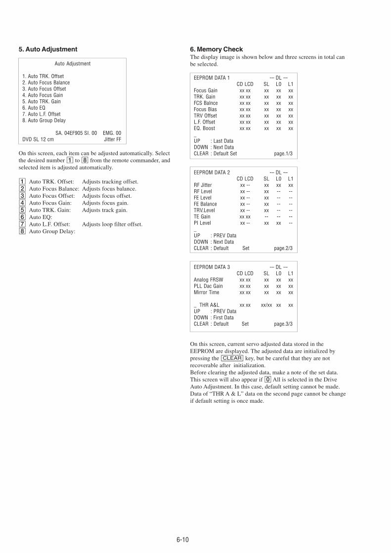
5. Auto Adjustment
Auto Adjustment
1. Auto TRK. Offset2. Auto Focus Balance3. Auto Focus Offset4. Auto Focus Gain5. Auto TRK. Gain6. Auto EQ7. Auto L.F. Offset8. Auto Group Delay
SA. 04EF905 SI. 00 EMG. 00DVD SL 12 cm Jitter FF
On this screen, each item can be adjusted automatically. Selectthe desired number 1 to 8 from the remote commander, andselected item is adjusted automatically.
1 Auto TRK. Offset: Adjusts tracking offset.2 Auto Focus Balance: Adjusts focus balance.3 Auto Focus Offset: Adjusts focus offset.4 Auto Focus Gain: Adjusts focus gain.5 Auto TRK. Gain: Adjusts track gain.6 Auto EQ:7 Auto L.F. Offset: Adjusts loop filter offset.8 Auto Group Delay:
6. Memory CheckThe display image is shown below and three screens in total canbe selected.
EEPROM DATA 1 -– DL -–CD LCD SL L0 L1
Focus Gain xx xx xx xx xxTRK. Gain xx xx xx xx xxFCS Balnce xx xx xx xx xxFocus Bias xx xx xx xx xxTRV Offset xx xx xx xx xxL.F. Offset xx xx xx xx xxEQ. Boost xx xx xx xx xx_UP : Last DataDOWN : Next DataCLEAR : Default Set page.1/3
EEPROM DATA 2 -– DL -–CD LCD SL L0 L1
RF Jitter xx -- xx xx xxRF Level xx -- xx -- --FE Level xx -- xx -- --FE Balance xx -- xx -- --TRV.Level xx -- xx -- --TE Gain xx xx -- -- --PI Level xx -- xx xx --_UP : PREV DataDOWN : Next DataCLEAR : Default Set page.2/3
EEPROM DATA 3 -– DL -–CD LCD SL L0 L1
Analog FRSW xx xx xx xx xxPLL Dac Gain xx xx xx xx xxMirror Time xx xx xx xx xx
_ THR A&L xx xx xx/xx xx xxUP : PREV DataDOWN : First DataCLEAR : Default Set page.3/3
On this screen, current servo adjusted data stored in theEEPROM are displayed. The adjusted data are initialized bypressing the [CLEAR] key, but be careful that they are notrecoverable after initialization.Before clearing the adjusted data, make a note of the set data.This screen will also appear if - All is selected in the DriveAuto Adjustment. In this case, default setting cannot be made.Data of “THR A & L” data on the second page cannot be changeif default setting is once made.

6-11
6-6. MECHA AGING
### Mecha Aging ###
Press OPEN key
Abort: STOP key
On the Test Mode Menu screen, selecting 3 executes the agingof mechanism. First, open the tray and load a disc. Pressthe H key, and the aging will start. During aging, the numberof the repeat cycle is displayed. Aging can be aborted at anytime by pressing the x key. After the operation has stopped,unload the disc and press again the x key or the [ RETURN]key to return to the Test Mode Menu.
6-7. EMERGENCY HISTORY
### EMG. History ###
Laser Hours CD xxhxxmDVD xxhxxm
1. 00 00 00 00 00 00 00 0000 00 00 00 00 00 00 00
2. 00 00 00 00 00 00 00 0000 00 00 00 00 00 00 00
Select: 1-9 Scroll: UP/DOWN(1: Last EMG.) Exit: RETURN
On the Test Mode Menu screen, selecting 4 displays theinformation such as servo emergency history. The historyinformation from last “1” up to “10” can be scrolled with $ keyor 4 key. Also, specific information can be displayed bydirectly entering that number with the ten-key pad from 1 to9.(Emergency history code is shown separately.)The upper two lines display the laser ON total hours. Databelow minutes are omitted.
Clearing History InformationClearing laser hoursPress [DISPLAY] and [CLEAR] keys in this order.Both CD and DVD data are cleared.Clearing emergency historyPress [TOP MENU] and [CLEAR] keys in this order.Initializing set up dataPress [MENU] and [CLEAR] keys in this order.The data have been initialized when “Set Up Initialized”message is displayed.The EMG. History display screen will be restored soon.
O
6-8. VERSION INFORMATION
### Version Infomation ###
IF con. Ver.x.xxx(xxxx)Group xx
SYScon. Ver.x.xxx(xxxx)Model xxRegion 0x
Servo DSP Ver: x.xxx AVD ucode Ver: xxxxxxxx
Exit : RETURN
The ROM version, region code, etc. are displayed if 5 isselected in the Test Mode Menu. The parenthesized hexadecimalnumber in the version number field indicates the checksumvalue of the ROM.
* Note after DownloadingAfter downloading ROM data, sometimes it happens thatchecksum is not the same as that of ROM data that has beendownloaded. In such a case, go back to the menu screen andselect “0. Syscon Diagnosis”, then select “1. All” in “2.Version”. If the result of this operation does not give anagreement, it must be either Download error or ROM error.
6-9. VIDEO LEVEL ADJUSTMENT
On the Test Mode Menu screen, selecting 6 displays color barsfor video level adjustment. During display of color bars, OSDdisappears but the menu screen will be restored if pressing anykey.

6-12
6-10. IF CON SELF DIAGNOSTIC FUNCTION
1. AF-98 BOARD (IF CON) TEXT MODEThe AF-98 board (IF CON) test mode is the IF CON self-diagnosis mode. THe IF CON can diagnose the functions of theAF98 board that the IF CON controls. Normally, the IF CONmakes a serial communication with the SYSTEM CONTROLand operates following the commands from the SYSTEMCONTROL, but in the Test mode, the IF CON operatesindependently from the SYSTEM CONTROL.
In the test mode, the following functions can be checked.1. Button function2. Remote commander receiving function3. SYSTEM CONTROL-IF CON serial communication4. Clisk shuttle function5. Fluorescent display tube lighting check
Grid checkAnode check
6. LED control function
In the test mode, the main unit operates same as usual, exceptvoltage monitoring, communication, display of fluorescentdisplay tube, and LED control.1. Theroutine that monitors +3.3V (PCONT) of MB-108 board
is not provided.2. The monitoring timer for serial communication with the
SYSTEM CONTROL is not provided. The main unit is notplaced in the Standby mode, even if the communication withSYSTEM CONTROL is normal.
3. Display of fluorescent display tube.(Normally, display is mode following the commands fromSYSTEM CONTROL).
4. LED control.(Normally, control is mode made following the commandsfrom SYSTEM CONTROL).
2. OPERATION OF SELF CHECK MODEThe Self Check mode is the function to conduct the basic test tothe FL display and DVD panel section.
2-1. Self Check Mode Transition ProcessingAt the AC Power ON after reset of IF CON is released with theMB-108 board are not connected to the AF-98 board, or whilepressing the x key on the main unit with the IF CON inSTANDBY mode, enter [RETURN] t [DISPLAY] (or [SETUP])on the remote commander, and the main unit transits to the SelfCheck Mode.

6-13
2-2. Operation of Auto Self CheckWhen the Self Check mode becomes active at the AC Power ON or by key input, the test display of the following steps (1) to (4) isrepeated.
(1) FLD and LED all ON (for 5 seconds)
(2) MODEL display (for 2 seconds)
(3) Version display (for 2 seconds)
(4) ROM creation date display (for 2 seconds)

6-14
2-3. Each Self Check FunctionEach Self Check function tests the FLD display, LED display, and key
input.
2-3-1. FLD and LED All ON2-3-1-1. Transition Keys in Self Check Mode• Z key and x key on the main unit• T key on the main unit and the remote commander
2-3-1-2. Operation and displayIn this mode, all LEDs except STANDBY LED and all segments of
FLD turn ON.
• Example of FLD all ON
2-3-2. Main Unit Key Name Display and Key Code Display2-3-2-1. Transition Keys in Self Check Mode• Keys on the main unit except keys transited in Self Check Mode
2-3-2-2. Operation and DisplayWhen a key on the main unit is pressed in the Self Check mode, thename of that key is displayed on the FLD. Aslo, the key name displayand the key code display can be switched with the [DISPLAY] key onthe remote commander, “NOTHING” is displayed when nothing isentered. Aslo, VIDEO CD, DVD, and CD segments turn on when acommunication error occurred.
• FLD display (at input of H key on the main unit)
InputVoltage [V]
IC404: Pin No. (Signal)
PIN ed (BRNKEY) PIN ef (PLAY) PIN eg (O/C) PIN eh (TVS)
0 - 0.21 - PLAY OPEN/CLOSE PIC MODE
0.63 - 0.86 - NEXT - TVS
1.23 - 1.55 - PREVIOUS - -
1.9 - 2.25 - PAUSE - -
2.63 - 2.86 - STOP - -

6-15
• Key code display(at input of H key, key code: 0Ah)
• At input of faulty voltage
• When key is pressed double
2-3-3. Remote Commander Key Name Display and KeyCode Display2-3-3-1. Transition Keys in Self Check Mode• Remote commander keys except keys transited in Self Check Mode
2-3-3-2. Operation and DisplayWhen a key on the remote commander is pressed in the Self CheckMode, the name of that key is displayed on the FLD. Aslo, the keyname display and the key code display can be switched with the[DISPLAY] key on the remote commander. “NOTHING” is displayedwhen nothing is entered. Aslo, VIDEO CD, DVD, and CD segmentsturn on when a communication error occurred.
• Remote commander key name display (at input of X key)
• Remote commander key code display(at input of X key, key code:39h)

6-16
2-3-4. Communication Monitoring DisplayThe communication state is momitored and displayed while the keyname on the main unit and the remote commander is displayed.When the communication to the System Controller faired, VIDEO CD,DVD, nad CD segments turn on.
• Communication error display(at no input of key and remote commander)
• Communication error display(at code display without input of the remote commander)
2-3-5. FLD Anode Test Display and SHUTTLE ClickOperation Test2-3-5-1. Transition Keys in Self Check Mode• t key on the remote commander• SHUTTLE on the remote commander during Anode Test display
(This unit does not provide JOG/SHUTTLE, and therefore useanother DVD remote commander having the JOG/SHUTTLE)
2-3-5-2. Operation and DisplayThe Self Check Mode transits to this mode when t key is entered.This tests whether each segment turns on individually. Only the firstsegment of each grid of FLD turns on, and each time the SHUTTLE isentered, the segment of each grid switched in order. When SHUTTLEinput is clockwise, the segment switches in 1 - 2 -3 direction, orcounterclockwise it switches in 3 - 2- 1 direction.
• Display at the start of Anode Test
r (Input in CW direction)

6-17
2-3-6. FLD Grid Test Display and SHUTTLE Click OperationTest2-3-6-1. Transition Keys in Self Check Mode• R key on the remote commander• SHUTTLE on the remote commander during Grid Test display
(This unit does not provide JOG/SHUTTLE, and therefore useanother DVD remote commander having the JOG/SHUTTLE)
2-3-6-2. Operation and DisplayThe Self Check Mode transits to this mode when R key is entered.This tests whether each grid turns on individually. The first grid onlyof FLD turns on and other grid turn off. Each time the SHUTTLE isentered, the grid is switched in order. When SHUTTLE input isclockwise, the grid switched in 1 - 2 - 3 direction, or counterclockwiseit switches in 3 - 2 - 1 direction.
• Display at the start of Grid Test
2-3-7. LED Test Display2-3-7-1. Transition Keys in Self Check Mode• r key on the remote commander• SHUTTLE on the remote commander during Grid Test display
(This model does not provide JOG/SHUTTLE, and therefore useanother DVD remote commander having the JOG/SHUTTLE)
2-3-7-2. Operation and DisplayLED is switched in order by the input JOG/SHUTTLE on the remotecommander. Aslo, LED ON/OFF is switched by the input of same keyas the function that turns on the LED conncerned.
• FLD display during LED Test
r (Input in CW direction)

6-18
2G 1G 7G 6G 5G 4G 3G 2G 1G
a
d
e
r
g
f
h k
j
s
n
pc
m
b
Dp
col
(7G-1G)
ANODE CONNECTION
P1
P2
P3
P4
P5
P6
P7
P8
P9
P10
P11
P12
P13
P14
P15
P16
P17
P18
P19
P20
7G 6G 5G 4G 3G 2G 1G
col col
a a a a a a a
h h h h h h h
j j j j j j j
k k k k k k k
b b b b b b b
f f f f f f f
m m m m m m m
s s s s s s s
g g g g g g g
e e e e e e e
n n n n n n n
p p p p p p p
r r r r r r r
c c c c c c c
d d d d d d d
Dp Dp Dp Dp Dp Dp Dp

6-19
6-11. TROUBLESHOOTING6-11-1. Cannot Enter Test ModeYou cannot enter the Test mode when either button has been pressedby any reason with the board assembled in the front panel. In thisstate, the power does not turn on even under normal condition (theunit is kept in standby state), and also no button is active and theremote commander is not accepted. In this case, disconnect theMB-108 board and AF-98 (CN601) board, and with the SELFCHECK (pin 0) of IF CON (IC404) on the AF-98 board kept inlow state, supply AC, and the IF CON self-diagnosis mode will beforcibly activated. The IF CON (IC404) checks the SELF CHECKport only after the power on reset (only at AC supply, not in standbystate). If any button is pressed, its name is displayed on thefluorescent display tube. But, if other than “NOTHING” isdisplayed though no button is pressed, it means that any buttonhas been pressed.
6-11-2. Faults in Test Mode (MB-108 board)1. The test mode menu is not displayed.1-1. Board visual check
Check that the ICs of SYSCON (IC104), ROM (IC106 orIC107), AVD (IC403), ARP & SERVO (IC301) are workingcorrectly.Check that outside appearance of the ICs is normal.Check that IC pins are not short-circuited.Check that there is no soldering error.Check that outside appearance of the capacitors and resistorsis normal.
1-2. Power supply voltage checkCheck the power voltage of the power connector (CN102).Check the power voltage of SYSCON (IC104).Check the power voltage of ROM (IC106 or IC107).Check the power voltage of AVD (IC403).Check the power voltage of ARP & SERVO (IC301).If the power voltage has any abnormality t
Check that the power supply lines are not shorted.Check that there is no soldering error.
If any abnormality cannot be found still tCheck that each IC is working normally.
1-3. Clock signal checkMeasure the clock signal frequency at CPUCK (CL101) ofSYSCON (IC104) with an oscilloscope.If the 8.25 MHz signal appears. t Check the machineaccording to section 1-3-1If the 33 MHz signal appears. t Check the machine accordingto section 1-3-2.If other frequencies are output.
R110 and R113 have defective soldering, X101 crystaloscillator is defective.
If the measurement point is fixed to either “H” or “L”. tObserve XFRRST (pin-uh) of SYSCON (IC104) with anoscilloscope.If the measurement point is “L”, check the following items.
If the IC has defective soldering, if the IC is short-circuited.If the measurement point is “H”,
t Component X101 or SYSCON (IC104) is defective.
1-3-1. When the 8.25 MHz signal appears at CPUCK• Check the XRD, XWRH and CS0X signal.
Observe XRD (pin-u;), XWRH (pin-ua), and CS0X (pin-tk)of SYSCON (IC104) with an oscilloscope.If these pins are fixed to either “L” (0V) or “H” (3.3V), or ifthese pins stay in the center voltage, check the followings.
Check if the signal line does not have the defectivesoldering.Check if the signal line is short-circuited with other signallines.If you cannot find any problem t SYSCON (IC104) isdefective.
• HA [0 to 21] signal and HD [0 to 15] signal checkObserve HA [0 to 21] (pins-<z/x to <z/. , <zzz to <zz, , <zx/ , 1 to 5)of SYSCON (IC104) and HD [0 to 15] (pins-ig to <z// ) withan oscilloscope.If these pins are fixed to either “L” (0V) or “H” (3.3V), or ifthe HA pin stays in the center voltage, check the followings.(HD stays in the center voltage when it is normal.)
t Check if the signal line does not have the defectivesoldering, or is short-circuited with other signal line orSYSCON (IC104) is defective.
• Reset signal checkCheck if XFRRST (pin-uh) of SYSCON (IC104) normal ornot.The signal starts up at the same time as Vcc t Defectivesoldering.
If the trouble does not apply to any of the above-describedphenomenon, SYSCON (IC104) or ROM (IC106 or IC107) isdefective.

6-20
1-3-2. When the 33 MHz signal appears at CPUCK• WAIT signal check
Observe XWAIT (pin-yj) of SYSCON (IC104) with anoscilloscope.If it is fixed to “L” (0V). t Observe CS2X to CS5X (pins-y; to yd).If CS2X or CS3X is “L”. t AVD (IC403) has defectivesoldering or AVD is defective.If CS4x or CS5X is “L”. t ARP & SERVO (IC301) hasdefective soldering or ARP & SERVO is defective.If any one of the above is not “L”. t XWAIT or CSnX isshort-circuited or has the defective soldering or AVD (IC403)is defective or ARP & SERVO (IC301) is defective.Center voltage t The XWAIT line has defective solderingor is short-circuited or AVD (IC403) is defective or ARP &SERVO (IC301) is defective or SYSCON (IC104) is defective.
• CSnX signal checkObserve CS0X to CS5X (pins-tk to yd) of SYSCON (IC104)with an oscilloscope.If they are fixed to “L” (0V) or if to center voltage t Checkthat the ICs do not have the defective soldering or is short-circuited with the other signal lines or SYSCON (IC104) isdefective.
CS0X: ROM (IC106 or IC107)CS2X, CS3X: AVD (IC403)CS4X, CS5X: ARP & SERVO (IC301)
If the trouble symptom does not apply to any of the abovephenomenon, SYSCON (IC104) or ROM (IC106 or IC107) isdefective.
2. Test mode menu is displayed but the machine stopswhen menu is selected2-1. AVD (IC403) check
Observe SDCLKO (pin-<zb, ) of AVD (IC403) with anoscilloscope.95 MHz t No problem27 MHz t Observe the XRST, HA, HD, XRD, XWRH INTand CS signal waveform at the respective pins of AVDEC,AVD (IC403) is defective.If the signal is other than the above frequencies t AVD(IC403) 27MHz signal line (CLKI (pin-<zb, ), SCLKIN (pin-<zn/ )) is short-circuited, IC mount is defective, AVD (IC403)is defective, PLL (IC103) is defective.
2-2. INT signal checkObserve INT0 to 2 (pins-qh to qk) of SYSCON (IC104) withan oscilloscope.If they are fixed to “L” (0V) or fixed to the center voltage tCheck that the ICs do not have the defective soldering, or areshort-circuited, SYSCON (IC104) is defective, or thefollowing ICs are not defective.
INT0: AVD (IC403)INT1, INT2: ARP & SERVO (IC301)
2-3. If any abnormality cannot be confirmed by theabove-described checks, check the CS signal thatis currently output.
The CS signal other than CS0X is being output. t IC mountis defective or the IC is defective depending on the movingCS signal.
CS2X, CS3X: AVD (IC403)CS4X, CS5X: ARP & SERVO (IC301)
If the trouble is not applicable to any of the above phenomenon,SYSCON (IC104) or ROM (IC106 or IC107) is defective.
3. If the message “SDSP No Ack” appears after the menuis displayed.
3-1. ARP & SERVO clock signal checkCheck frequency of CLKIN (pin-<zb/ )33 MHz t NormalFrequency other than 33 MHz t CLKIN is short-circuitedor defective soldering or PLL (IC103) is defective or ARP &SERVO (IC301) is defective
3-2. ARP & SERVO (IC301) PLL oscillation checkObserve PLCKO (pin-ij) of ARP & SERVO (IC301) withan oscilloscope.If the pin is fixed to either “L” (0V) or “H” (3.3V).
If XRST if fixed to “L”. XRST has the defective soldering,In all other cases. ARP & SERVO (IC301) is defective
If it is oscillating.HA [0 to 7] are HD [8 to 15] are short-circuited, checkXSDSPIT and XSDSPCS or ARP & SERVO (IC301) isdefective.
4. If trouble occurs at the specific item of the “Diag AllCheck”.
IC mount of the NG item is defective or IC is defective.
5. Picture and audio are not output.Check connection of CN601Check for the defective connection of flat cable and check ofdamage of the flat cable.
6. Picture is output but audio is not output.Check the audio data output (at pins-wf, wk, and wl) of AVD(IC403)
The audio data is not output. t AVD (IC403) or audioDAC (IC601) mount is defective or power supply isdefective or AVD (IC403) or audio DAC (IC601) isdefective.
PLL (IC103) 512fs output checkIf the frequency or waveform has abnormality. t Thesignal line has defective soldering or the signal line is short-circuited with other signal lines or PLL (IC103) isdefective.
7. Audio is output but picture is not output.Observe pins-tg, tj, tl, ya, yd and yg of AVD (IC403) withan oscilloscope.If the analog signal is not output. t The signal line has thedefective soldering or is short-circuited or parts are defectiveor AVD (IC403) is defective.
6-11-3. Drive Auto Adjustment stops due to error.The ARP & SERVO (IC301) analog circuit of MB-108 board isdefective or RF-Amp (IC201) or M-Driver (IC202) peripheralcircuit is defective or optical pickup block is defective or flat cableconnection is defective

6-21
6-11-4. The product itself is defective.• If MB108 does not have any problem,
The board other than MB-108 board is defective orconnection is defective or optical pickup block is defectiveor mechanism deck is defective
1. FL display does not light when the POWER buttonis pressed.
1-1. Check the EVER -15.5V (pin-2), EVER+5.0V(pin-qa), EVER+11V (pin-qd) voltage at CN201 ofthe power supply block/
If voltage is abnormal. t The power supply block isdefective.
1-2. Check if the fuse on the IF board has blown ofnot.
If the fuse has blown t Replace the fuse.
1-3. Check the P-CONT (pin-2) at CN401 of the AF-98board when the POWER button is pressed.
If it remains at “L”,t The signal line has the defective soldering or it is short-circuited with other signal lines or capacitor or resistor isdefective or IFCON is defective or connection between thepower supply block and the AF-98 board is defective, orconnector installation is defective, or the power supplyblock is defective.
1-4. Check if the button is kept depressed in theIFCON self mode.
If the button is kept depressed. t The front panel isdefective, or AF-98 board is defective.
1-5. Check PONCHK (pin-e;) of IFCON (IC404) on theAF-98 board.
If it is 0.5 V or more. t The power supply is defective, orAF-98 board is defective.
1-6. Check ND401 (pin-1 & pin-ek) on the AF-98board.
If no voltage supply t Voltage driver (IC407) defective, orthe AF-98 board is defective.
2. FL display light once and becomes not light whenPOWER button is pressed.
2-1. Check CN201 voltage of the power supply blockwhen the FL display light on.
If voltage is abnormal. t The power supply block isdefective, or the AF-98 board is defective, or MB108 isdefective
2-2. Check XFRRST (pin-8) at CN101 on the MB-108board.
If it is fixed to “L”. t The signal line has defectivesoldering, or is short-circuited with other signal lines, orparts are defective.
2-3. Check IFBSY (pin-5), XIFCS (pin-6), SI0 (pin-4),SO0 (pin-1) and SC0 (pin-3) at CN101
If they are fixed to “H” or “L”.t The signal line has defective soldering, or is short-circuited with other signal line, or parts are defective, orSYSCON (IC104) is defectiveIf they change between “L/H”.Connector installation is defective, or the AF-98 board isdefective, or SYSCON (IC104) is defective.If they stay in the center voltage.Poor connection of flexible wiring board such as it isinserted in an angle diagonally, or defective soldering, or isshort-circuited with other signal line.
2-4. Check PONCHK (pin-e;) of IFCON (IC404) on theAF-98 board.
If rise-up time from 0.5 V to 1.5 V or more takes longertime, or it does not exceed 1.5 V or more. t The AF boardis defective.
3. Both picture and audio are not output.Connection between the power supply block and the AF-98board is defective, or connection between the AF-98 boardand the MB-108 board is defective, or connector installationis defective, or AF-98 board is defective.
4. Picture is not normal. (Block noise or othersappear.)
The MB-103 board AVD (IC403) or SDRAM (IC404,IC405) is defective, or ARP & SERVO (IC301) is defective.

7-1
7-1. POWER SUPPLY CHECKETXNY410M0F NS325 : PX, E, BR, AR
NS530 : HK, SP, TW, KR, ME, AUSNS725P : PXNS730P : HK, SP, KR, ME, AUS
ETXNY410E0F NS330 : AE, UK, RUNS333 : AENS730P : AE, UKNS733P : AE
HS8S2U NS325 : US, CND, MXNS725P : US, CND
Mode E-E
Instrument Digital voltmeter
EVER +5.0 V Check
Test point CN201 pin qa
Specification 5.0 ± 0.3 Vdc
SW +3.5 V Check
Test point CN201 pin 0
Specification 3.5 ± 0.2 Vdc
SW+5 V Check
Test point CN201 pin qs
Specification 5.0 ± 0.3 Vdc
SW +11 V Check
Test point CN201 pin 5, 6
Specification 11.0 ± 1.0 Vdc
EVER +11 V Check
Test point CN201 pin qd
Specification 11.2 ± 1.0 Vdc
EVER –15.5 V Check
Test point CN201 pin 2
Specification –15.5 ± Vdc
Checking method:1) Confirm that each voltage satisfies the specification.
NoteBecause the heatsink installed on the power supply board is apart of the primary side, never touch it to avoid electrical shock.
AbbreviationUS : USA modelCND : Canadian modelPX : PX modelE : Latin AmericaMX : Mexico modelBR : Brazilian modelAR : Argentina modelHK : Hong Kong modelSP : Malaysia, Thai, Philippine, Indonesia, Vietnam modelsTW : Taiwan modelKR : Korea modelEA : Saudi Arabia modelME2 : Middle East modelME5 : India, Pakistan, Morocco modelsAUS : Australian modelCN : Chinese modelUK : UK modelRUS : Russian modelAE1 : AEP modelAE2 : AEP model
SECTION 7ELECTRICAL ADJUSTMENT
DVP-NS325/NS330/NS333/NS430/NS433/NS530/NS725P/NS730P
In making adjustment, refer to 7-3. AdjustmentRelated Parts Arrangement.
This section describes procedures and instructions necessary foradjusting electrical circuits in this set.
Instruments required:1) Color monitor TV2) Oscilloscope 1 or 2 phenomena, band width over 100 MHz,
with delay mode3) Frequency counter (over 8 digits)4) Digital voltmeter5) Standard commander (RMT-D126J)6) DVD reference disc
HLX-501 (J-6090-071-A) (dual layer) (NTSC)HLX-503 (J-6090-069-A) (single layer) (NTSC)HLX-504 (J-6090-088-A) (single layer) (NTSC)HLX-505 (J-6090-089-A) (dual layer) (NTSC)
7) SACD reference discHLXA-509 (J-6090-090-A)
8) Extention Cable (J-6090-107-A)
–7.0+1.0

7-2
1.0 Vp-p +0.04–0.02
3. Checking S Video Output S-C<Purpose>This checks whether the S video output S-C satisfies the NTSCstandard. If it is not correct, the colors will be too dark or toolight.
Mode Video level adjustment in test mode
Signal Color bars
Test point S VIDEO OUT (S-Y) connector(75 Ω terminated)
Instrument Oscilloscope
Specification 1.00 ± 0.05 Vp-p
Checking method:1) In the test mode initial menu “6” Video Level Adjustment, set
so that color bars are generated.2) Confirm that the S-C burst is 286 ± 30 mVp-p.
Figure 7-3
4. Checking Component Video Output Y<Purpose>This checks component video output Y. If it is incorrect, correctbrightness will not be attained when connected to, for instance,projector.
Mode Video level adjustment in test mode
Signal Color bars
Test point COMPONENT VIDEO OUT (Y)connector, D1 VIDEO OUT connector,Pin 1 (75 Ω terminated)
Instrument Oscilloscope
Specification 1.0 ± 0.05 Vp-p
Checking method:1) In the test mode initial menu “6” Video Level Adjustment, set
so that color bars are generated.2) Confirm that the S-C burst is “A”.
Figure 7-4
7-2. ADJUSTMENT OF VIDEO SYSTEM1. Video Level Adjustment (MB-108 BOARD)<Purpose>This adjustment is made to satisfy the NTSC standard, and if notadjusted correctly, the brightness will be too large or small.
Mode Video level adjustment in test mode
Signal Color bars
Test point LINE OUT (VIDEO) connector(75 Ω terminated)
Instrument Oscilloscope
Adjusting element RV501
Specification 1.00 Vp-p
Adjusting method:1) In the test mode initial menu “6” Video Level Adjustment, set
so that color bars are generated.2) Adjust the RV401 to attain 1.00 Vp-p.
Figure 7-1
2. Checking S Video Output S-Y<Purpose>Check S-terminal video output. If it is incorrect, pictures will notbe displayed correctly in spite of connection to the TV with a S-terminal cable.
Mode Video level adjustment in test mode
Signal Color bars
Test point S VIDEO OUT (S-Y) connector(75 Ω terminated)
Instrument Oscilloscope
Specification 1.0 ± 0.05 Vp-p
Checking method:1) In the test mode initial menu “6” Video Level Adjustment, set
so that color bars are generated.2) Confirm that the the S-Y level is 1.0 ± 0.05 Vp-p.
Figure 7-2
+0.04–0.02
+0.04–0.02
1.0 ± 0.05 Vp-p 1.0 ± 0.05 Vp-p
286 ± 30 mVp-p

7-3
5. Checking Component Video Output B-Y<Purpose>This checks component video output B-Y. If it is incorrect,correct color will not be displayed when connected to, for instance,component input projector.
Mode Video level adjustment in test mode
Signal Color bars
Test point COMPONENT VIDEO OUT (CB)connector, D1 VIDEO OUTconnector, Pin 3 (75 Ω terminated)
Instrument Oscilloscope
Specification A = 700 ± 50 mVp-p (others)646 ± 50 mVp-p(For Us, Canada)
Checking method:1) In the test mode initial menu “6” Video Level Adjustment, set
so that color bars are generated.2) Confirm that the B-Y level is A.
Figure 7-5
6. Checking Component Video Output R-Y<Purpose>This checks component video output R-Y. If it is incorrect,correct color will not be displayed when connected to, for instance,component input projector.
Mode Video level adjustment in test mode
Signal Color bars
Test point COMPONENT VIDEO OUT (CR)connector, D1 VIDEO OUTconnector, Pin 5 (75 Ω terminated)
Instrument Oscilloscope
Specification B = 700 ± 50 mVp-p (others)646 ± 50 mVp-p(For Us, Canada)
Checking method:1) In the test mode initial menu “6” Video Level Adjustment, set
so that color bars are generated.2) Confirm that the R-Y level is B.
Figure 7-6
BA