0 fermi national accelerator laboratory -...
TRANSCRIPT
0 Fermi National Accelerator Laboratory
FERMILAB-Pub-87/183-E [E-741/CDF]
The CDF Vertex Time Projection Chamber System*
F. Snider University of Chicago
Chicago, Illinois 60637, USA
M. Binkley, J. Huth, R.‘Kephart, C. Newman-Holmes, S. Palanque*, J. Patrick, R. Yarema, G. P. Yeh, and T. Zimmerman
Fermi National Accelerator Laboratoryt P.O. Box 500, Batavia, Illinois 60510, USA
M. Schub Purdue University
West Lafayette, Indiana 47907, USA
F. Abe’, K. Kondo, T. Mimashi, and M. Sekiguchi Institute of Physics. University of Tsukuba
Sakura, Niihti, lbaraki 305, Japan
July-August 1987
*Submitted to Nucl. Insuum. Methods A
e Operated by Universities Research Association Inc. under contract with the United States Department of Energy

The CDF Vertex Time Projection Chamber System
F. Snider
University of Chicago
Chicago, Illinois 80837,USA
M. Biiley, J. Huth, R. Kephart, C.Newman- Holmes, S. Palanque l
J. Patrick, R. Yarema, G.P. Yeh, and T. Zimmerman
Fermi National Accelerator Laboratory’
Batavia, Illinois 80510, USA
M. Schub
Purdue University
W. Layfayette, IN, 47907
F. Abe 1, K. Kondo, T. Miiaahi, M. Sekiguchi
Institute of Physics, University of Tsukuba
Sakura, Niiiari, Ibaraki 305, Japan
June 12, 1987
Abstract
The Vertex Tic F’rojection Chamber (VTPC) system is one of the major components
of the charged particle trdhg +m for the Collidv Detector at Fermilab (CDF).
The chambera cover about seven units of pseodwrapidity ( q )and must be capable of
handling substantially more than the SO-55 charged particle traclm produced by typical
jip collisions at CM energies of 1.8 TeV. The chambers M optimiied to provide the good
-m, h~.cfmm CEN S.c,., DPdPE - STlPE
t0p.nte.t h, “,,t.emttta Racueh A.socbtton ondrr Contr.ct with the U.S. Department of Emrg No. DE-AC02-76CH03000
:N.,bbnd L.b. ior Bfib Emera Pb,r, KEK , Ohomlchl, Tmkob.-PI,, Dmra”-ken, 305, hpm
1
pattern recognition in the r-z view required to locate the event vertex, measure the ov~all
event topology, and to complement the r-0 tracking in the large axial wire drift chamber
that swrolmds them. The chambera provide r-s information using TDC data from sense
wire sign& hform~ian on the 4 of tracks ia obtained fmm cathode pad signab on
. l bsct of chambera red out by a FADC system. A rim&r ayystem mc~urw dE/dz of
tracks in the forward COIWE snnounding the exiting beams. Because of the large number of
photona that pass through the detector during each collision, novel techniques are required
to reduce the amount of material in the chamha. These techniques include a custom
surface mount integrated eircnit preampliliu, epoxy-graphite and Kapton covered foam
atroctud members, and miniature coaxial signal cables The mechanical construction
of the chamber, radiation length YS angle, and details of the electronica are dacribed.
The event reconstruction, corrections, and preliminary performance results for 1.8 TeV @
colliaiolu are also diinsaed.
1 Design Requirements
The VTPC (Vertex Tie Projection Chamber) system consists of eight double time
projection chambers surrounding the beam pipe and mounted end-t-end along the
beam direction (x-axis). The Iocation of the VTPC in the CDF central detector
[1] is shown in Figure 1. The VTPC contributes both stand-alone tracking and
measurements which complement those obtained with the Central Tracking Chamber
(CTC) [2] and the Forward Tracking Chambers (FTC)[3].
The basic design requirements of the VTPC system were:
1. Provide z-vertex determination. The distribution of event vertices at the Teva-
tron collider is a Gaussian along the beam axis with a typical FWHM of 75 cm.
Knowledge of the location of the event vertex is a first order correction in the
1

calculation of physics quantities such as the transverse energy and is the starting
point for offline event reconstruction.
2. Determine overall event topologies over a very wide range in polar angles (3.5’ <
8 < 176.5”), and perform various charged particle measurements such as
< Nen >TCJT~ and dNd/dq for -3.5 < n < 3.5.
3. Identify multiple interactions in the same beam crossing. When the Tevatron ia
operated in three bunch mode at a luminosity of lO%m-‘s-r at least one event
in five will contain a multiple interaction. This requires good pattern recognition
in the r-z plane in eve&u often containing a hundred or more charged particle
tracks.
4. Detect charged particle tracks near the vertex where the amount of material
traversed ia still small. This ia important in order to minimize photon conversion
contamination of electrons.
5. Provide intermediate angle tracking (10” < B < 30”) . In this angular region
VTPC information is used in conjunction with limited CTC information to pro-
vide both pointing and momentum measurements. This ie essential for e/no
separation in the endplug calorimetry.
6. Provide forward angle tracking (3.5’ < 0 < 10”). The VTPC wire informa-
tion must provide pointing in the r-z projection for the forward calorimetry.
Similarly, the pad r-4 reconstruction can be used in conjunction with FTC in-
formation to determine the sign of the charge of forward particles, particularly
leptons. In addition, a rough momentum measurement is possible for low rn*
mentum particles in this region.
s

7. Finally, to minimize the effects on other tracking systems Gom secondary inter-
actions and multiple scattering, the entire VTPC system must be very thin in
terma of radiation lengths.
2 Chamber Design
Each of the eight octagonal VTPC modules has a central high voltage grid that
divides it into two 15.25 cm long drift regions. It is eventually planned to operate
the Tevatron in six bunch mode with 3.5 /,LS between crossings. The 15.25 cm drift
length ia chosen so that the maximum drift time is less than 3.5 JM when the drift
velocity in the gas ia 46 pm/ns (eg. argon-ethane 50/50 at atmospheric pressure and
E=320 V/cm). The electrons drift away from the center grid until they pass through
a cathode grid and enter one of the two proportional chamber endcaps. Each endcap
is divided into octants, with 24 sense wires and 24 cathode pads in each octant. The
arrival times of the electrons at the sense wires give a picture of the event in the r-z
plane. In addition the sense wires and pads in some endcaps are instrumented with
an analog pulse height readout using Flash Analog to Digital Converters (FADC), so
that dE/dz and 4 information is available for particles produced at angles between 5”
and 25” with respect to each beam axis. Two VTPC modules are shown in Figure 2.
Adjacent modules have a relative rotation angle of 4. = arctan (.2) about the beam
axis. For tracks passing through at least two modules, this eliminates inefficiencies
near octant boundaries and provides 4 information from small angle stereo.
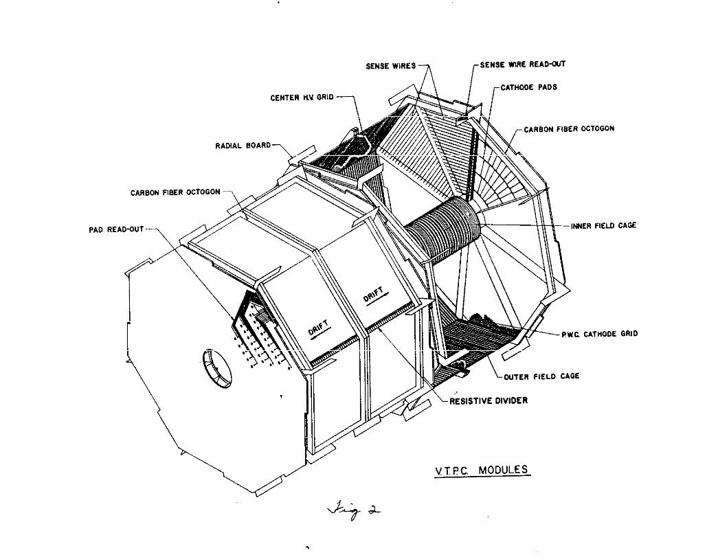
Aa viewed from the drift region, an octant consists of a cathode grid followed
by a plane of field shaping wires, a plane of sense wires, and a resistive ink cathode
4

plane. Three rows of pads are located behind the resistive cathode, separated by 150
pm of epoxy-fiberglass (GlO). A pad covers 4.12 cm in radius and 1.4 cm in r-4.
The sense wire plane is 1 cm from both the cathode grid and resistive cathode, and
the plane of field shaping wires is offset by 3 mm toward the cathode grid from the
sense wire plane. The apscing between both field shaping wires and sense wires is
6.34 mm. The field shaping wires are offset by l/2 wire spacing in r with respect
to the sense wires. Since the sense wires in each octant are read out separately, the
wires in adjacent octants are offset radially by l/2 wire spacing. The active area of
the chamber extends from about I = 7 cm to r = 21 cm. A more detailed view of
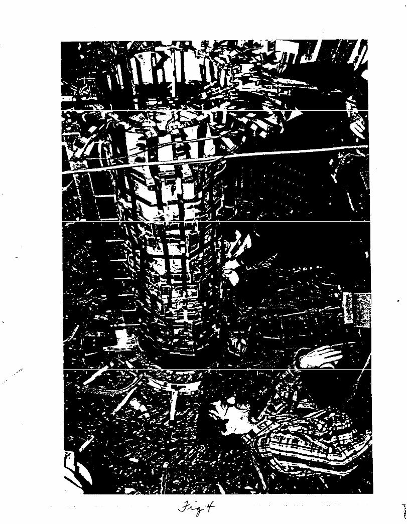
the proportional chamber portion of the VTPC is shown in Figure 3. Figure 4 is a
photograph of four VTPC modules in their service position during installation. A
summsry of VTPC parameters is given in Table 1.
3 Low-mass Construction
An average of - 30 photons pass through the VTPC per event. Since the VTPC
is located inside the CDF central and forward tracking chambers, it is extremely
important to minimize the effective thickness of the chamber in radiation lengths.
Any photon conversions which do occur in the VTPC cm result in large local track
density in these systems and can make pattern recognition and track reconstruction
difficult or impossible. In addition, such conversions degrade the electron identi5-
cation capability of the experiment and the multiple Coulomb scattering adversely
affects the CTC momentum resolution. As a result the materials used in constructing
the VTPC were chosen with particular emphasis toward low mass and long radiation
5

length. The mechanical structure of the VTPC consists mainly of such light-nuclei
materials as Rohacell foam [4], Kapton film [5], and epoxy-5ber laminates employing
either glass or graphite fibers. The basic technique is to use a core of lightweight
foam covered with a strong akin. This construction puts the denser material where it
contributes most to the moment of inertia and therefore provides the best atiffness-
t-mass ratio. The use of graphite fibers is particularly effective since they have
excellent strength, a high modulus, and a long radiation length.
The VTPC field cage assembly consists of a high voltage center grid and
two cathode grids supported by four octagonal epoxy-graphite/foam Games. These
frames are attached to the walls of the VTPC 5eld cage and provide a lightweight but
stiff base for the field cage structure. The 5eld cage walls are constructed of a three-
layer Kapton-foam-Kapton lamination that supports the 5eId shaping electrodes.
The electrodes are overlapping copper strips etched on both aides of the inner copper
clad Kapton skin. The Kapton ia 25 pm thick, the cladding is 16 pm of copper,
and the foam is 2 mm thick. Construction of the 5eld cage begins by prefabrication
of the field cage walls. The outer field cage is octagonal in shape, the inner wall
is cylindrical. The octagonal epoxy-graphite/foam frames are also prefabricated by
laying up a two layer laminate of 140 pm graphite 5bers impregnated with a Batage
epoxy [6] around a foam core and curing thii assembly in a precision mold at 15W
C for five hours. The cathode grids are made of stainless steel screen with 50 pm
wires on 500 firn centers[7]. The central high voltage grid employs screen with 50
pm wires on loo0 pm centers. The screens are stretched on a transfer fixture to a
tension of 160 N/m. The field cage walls, frames, and screens are then assembled
and glued on a machined alignment jig that controls the screen to screen spacing as
6

well as the electrode alignment to a precision of 50 pm. After assembly the transfer
fixture is removed and the epoxy-graphite Games then support the screen tension.
These Games also prevent the VTPC modules from deforming due to the stresses
of the mounting system and the weight of the cables. The precise screen-to-screen
spacing is maintained by 1.6 mm dia. ‘pultruded” glass rods [8] at each corner of
the octagonal 5eld cage.
The VTPC endcaps are fabricated with similar techniques. Ciuit boards
employing 150 pm thick epoxy-fiberglass laminates (GlO) form a sandwich with
3 mm thick foam to provide stiffness for the endcapa. The surface of one circuit
board is coated with a resistive polymer ink [Q] with a surface resistivity of about
10 MII/square. The other aide of this board is clad with 13.5 pm of copper. This
copper cladding is etched to provide the cathode readout pads. Connections to these
pads are made with conductive epoxy using copper strips passing through 6.4 mm
diameter holes in the foam to a readout board at the extreme ends of the module.
The pad preamplifiers are later mounted directly to this board. After the cathode
sandwich is complete, radial readout boards and thin GlO frames are glued to it in
another precision assembly fixture. These radial boards consist of a custom 0.74 mm
thick three-layer circuit board. The outer layers of this board are etched to provide
electric field shaping electrodes, as well M terminals to which both field shaping
and sense wires are soldered. The signals from the sense wires pass through plated-
through holes and are carried out radially on traces located in the middle of the circuit
board. At the outside radius the traces resurface and connect to the preamplifiers
mounted on the radial boards. After etching, the boards are laser machined in a
single setup that cuts them to shape and laser drills precision holes that determine
the 5eld shaping and sense wire locations. After the endcap assembly is removed
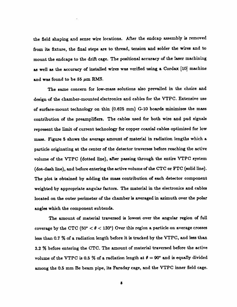
from its fixture, the final steps are to thread, tension and solder the wires and to
mount the endcapa to the drii cage. The positional accuracy of the laser machining
as well as the accuracy of installed wires was verified using a Cordax [lo] machine
and was found to be 55 pm RMS.
The same concern for low-mass solutions also prevailed in the choice and
design of the chamber-mounted electronics and cables for the VTPC. Extensive use
of surface-mount technology on thin (0.625 mm) GlO boards minimizes the mass
contribution of the preamplifiers. The cables used for both wire and pad signals
represent the limit of current technology for copper coaxial cables optimized for low
msss. Figure 5 shows the average amount of material in radiation lengths which a
particle originating at the center of the detector traverses before reaching the active
volume of the VTPC (dotted line), after passing through the entire VTPC system
(dot-dash line), and before entering the active volume of the CTC or FTC (solid line).
The plot is obtained by adding the mass contribution of each detector component
weighted by appropriate angular factors. The material in the electronics and cables
located on the outer perimeter of the chamber is averaged in azimuth over the polar
angles which the component subtends.
The amount of material traversed is lowest over the angular region of full
coverage by the CTC (50’ < 0 < 130”) 0 ver this region a particle on average crosses
less than 0.7 % of a radiation length before it is tracked by the VTPC, and less than
3.2 % before entering the CTC. The amount of material traversed before the active
volume of the VTPC is 0.5 % of a radiation length at 19 = 90’ and is equally divided
among the 0.5 mm Be beam pipe, its Faraday cage, and the VTPC inner field cage.

The traversed mass distribution peaks between 10-20” with respect to each exiting
beam with 6 % of a radiation length before, and 22 % after tracking by the VTPC
in the worst region. However, in this angular range, the VTPC provides nearly all
tracking information available. Thus the material after the VTPC active volume haa
a relatively small impact on other tracking systems. In the angular region covered by
the FTC (2’ < 6 < lo”), the amount of material crossed by a particle passing through
the VTPC drops to between 610 % of a radiation length. The discontinuitiea in the
plot correspond to places where a new set of cables ia added or a new proportional
chamber traversed. The drop in effective thickness below 10” is due to the fact that
the signal cables exit the gas vessel at lo’, then pass between the CTC endplate
and the end plug calorimeter system, away from the path of particles pointing at the
FTC. In the current version of the VTPC, copper in cables and laminates contributes
a signiticrmt fraction of the total radiation length of the overall system. Alternatives
such (u vapor deposited copper, aluminum laminates and aluminum coaxial cables
were explored but thus far have proved unsatisfactory.
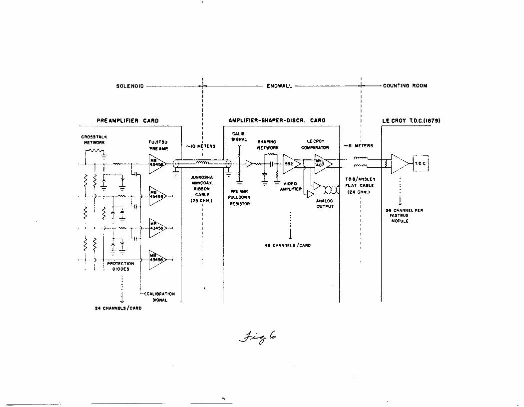
4 Electronics
The front end electronica for the VTPC consists of preamplifiers mounted directly
on the chambers, amplifier-shaper-discriminator (ASD) cards located on the central
detector endwalls, and FASTBUS TDCs and FADCa located in the counting room.
The preamplifiers are connected to the ASD cards by 10 m long miniature coaxial
cables. Each coax is 0.75 mm in diameter and ia contained in a 25 coax ribbon
cable custom manufactured for the VTPC system by Junkosha Co. Ltd Japan [ll].
9

The individual coax has an inner conductor with a resistance of 0.5 D/m (32 gauge
equivalent) and a shield with 0.27 D/ m. The characteristic impedance is 42 fl and
the rise time for the 10 meter length is about 5 ns (10% to 70%). The signals sent
Gom the ASD cards to the TDCs and FADCs in the counting room are differential.
The ECL level signals for the TDCa are sent on a 61 m long flat cable (polyethylene
dielectric) with two signal wires and one isolating ground wire per channel[l2]. The
FADC signals are sent on a round cable with 24 individually shielded twisted pairs
surrounded by a collective outer shield[l3]. Th e calibration system designed for
the CTC is used to generate test pulses and to monitor the stability of the VTPC
electronics [2].
4.1 Wire Electronica
The wire preamplifier is a fast grounded-base amplifier. To minimize mass, the
basic circuit is implemented on a custom integrated circuit using analog master slice
techniques [14]. The resulting chip (Fujitsu MB43458) contains four preamplifiers
on a single substrate in a 14 pin surface mount package. The 24 channel surface
mount preampli5er cards for the VTPC use six of these chips [15] and include both
protection diodes and a resistor network to cancel opposite sign cross-talk. The
ribbon coax cables are soldered directly to the preampli5er card in order to provide
a good low inductance ground connection. Power dissipation is an important design
consideration due to the difficulty of cooling the centrally located VTPC preamplifiers
without adding excessive material. The circuit dissipates about 25 mW per channel.
Each channel on the wire ASD card [2] consists of a pull-down resistor for
the preampli5er, an emitter follower, a shaping network, an amplifier, and a LeCroy
10

bfVL407 comparator [la]. The shaping network consists of a pole-zero alter which
cancels most of the long l/t tail of the signal (RC about 700 ns) and a short time
constant integrator (RC about 30 us) which widens the time window over which the
fast signala from different electrons are added. Computer simulations indicate that
the integration improves the resolution and reduces the number of excursions below
the comparator threshold for tracks at small angles with respect to the beams. The
comparator produces a time-over-threshold ECL logic signal that is sent to the TDC.
The TDCs are LeCroy 1879 FASTBUS modules with multihit capabilities. There are
512 time bins in the TDC, each time bin corresponding to about 320 pm. The TDCs
are read out using a modified version of the SLAC Scanner Processor (SSP) [17].
The average event taken with minimum trigger bias contains 8 kbytes of TDC data.
A schematic of this system is presented in Figure 6.
4.2 Pad Electronics
A simplified schematic of the VTPC pad electronics is shown in Figure 7. The
pad preamplifiers sre LeCroy HQV802 hybrid FET input charge sensitive amplifiers
custom packaged for the VTPC system with eight channels in a low msss plastic
case. These packages combine low msss (3.5 grams for eight channels), low power
consumption (about 60 mW per channel for our conditions), and low noise (about
1500 electrons equivalent for a 200 ns integration time). The hybrids are mounted
on a thin 24 channel circuit board containing protection diodes and a series back
termination resistor for each channel.
Each channel of the pad-amplifier-shaper (PAS) card has a pull-down resistor
for the preamplifier, a pole-zero filter, a four stage semi-Gaussian integrator, and an
11
smplifler. Emitter followers are used as needed for impedance transformation. The
pole zero filter is used to replace the 400 118 integration RC of the preamplifier with
a 40 ns RC (for a 6 function preamplifier input). Emh stage of the semi-Gaussian
integrator [18] adds another RC of about 35 ns. A very narrow input signal at the
preamplifier has a FWHM of about 170 ns at the PAS output. The purpose of the
integration is to reduce the high frequency noise that would otherwise be observed
due to the short sampling time of the FADC and to match the memory time of the
output waveform to the 10.6 MHz clock speed.
4.9 FADC System
The FADC system performs digitization of analog signals and compaction of the
digitized data. The system consists of a) 64 FADC modules (1536 channels total)
which digitize analog signals from PAS cards and b) eight compaction modules which
read and compact the digitized data from the FADC modules.
423.1 FADC Module
A FADC module contains 24 channels in a single width FASTBUS module. The
module uses the FASTBUS crate only for DC power and cooling. The analog signals
from PAS cards on the detector wall arrive at the FADC modules located in the
counting room. The signals are received by a line receiver based on an operational
amplifier and fed into an eight bit FADC chip (Sony CXAlOl6P). The analog baseline
is restored by an operational trausconductance amplifier (RCA CA3080E) which
removes charge accumulated on the final decoupling capacitor. The digitized data
from the FADC chip are continuously written into two ECL random access memories
11

(10422) until a stop signal is issued at the end of the VTPC drift time. A single
FADC module dissipates 77W total and can operate at clock speeds up to 35 MHz.
For the data described in this paper the FADC module was operated at a 10.6 MHz
sampling rate to reduce the total amount of data per event written to magnetic tape.
4.s.z compaction Module
A compaction module reads and compacts data from the FADC modules. Each
compaction module is a singIe width FASTBUS slave that communicates with eight
FADC modules through a dedicated external bus. After a stop signal, the FADCs
are read out and their data are compacted to form groups corresponding to FADC
data which are above a programmable threshold and which are contiguous in time.
Usually such a group is the result of one chamber pulse. A header word that describes
the channel address, time address, and the number of the FADC data points in the
group is added to each group. Since the typical signal from the chamber is quite long
(l-4 JM), this compaction method miniizes redundant address/time information.
The actual FADC values typically make up over 71% of the total formatted data.
The remainder is time-channel markers and headers. The average size of pad data for
1.8 TeV events taken with a mlniium bias trigger is 11-12 tbytes. The compaction
process requires 500 w per event. The compacted data is stored in local memory,
then read via FASTBUS through the SSP.
IS

5 Reconstruction and Systematics
6.1 wire ReconrtNction
A reconstruction program that uses the wire TDC information provides accurate
tracking of charged particles throughout the active volume of the VTPC. The recon-
struction algorithm has three steps. Track segments a tit identified in individual
chamber o&ants. Next, the intercepts of these track segments with the beam axis
are used to reconstruct the primary vertex location. Finally, tracks are found and
fit across octant and module boundaries. The first two steps are very fast requiring
about 300 ms of VAX 8650 CPU time per event. The information from these steps
is used for more than just subsequent VTPC reconstruction. The beam collision
point is monitored online using the VTPC vertex reconstruction. In addition, the
offline calculation of transverse energy corrections in the calorimetry uses thii ‘fast’
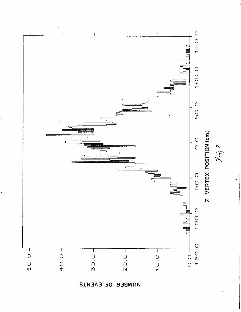
vertex location as does the CTC reconstruction. Figure 8 shows the distribution of
reconstructed event vertices for a typical run. The third step, track 5nding across
o&ant and module boundaries, begins by hiitogrrunming hits as a function of polar
angle with respect to the vertex found in step two. Primary tracks appear as spikes
in this histogram. The positions of these spikes determine roads used to associate
specific hits to a given track. These associated hits are then tit sepmately in modules
having the same 4 rotation angle. Finally, three-dimensional information is obtained
by combining these fit parameters for tracks crossing module boundaries. All tracks
are currently assumed linear. The effect of track curvature due to the axial magnetic
field is not observable in wire data for tracks with Pt > 300 MeV/c.
Thii multi-step procedure has the advantage that it uses a single algorithm to
14

6nd tracks over the large angular acceptance of the VTPC. As a result, reconstruction
efficiency should be smooth as a function of track angle. In addition, this procedure
has good efficiency in a high multiplicity environment and is sufficiently fast to allow
full reconstruction of a large number of events. The average reconstruction time for
events taken with minimum trigger bias is about 1.5 seconds and scales linearly with
the number of tracks in the event.
The Iong drift lengths, ExB forces on drifting electrons, and the wide range of
track polar angles seen by the VTPC result in several important systematic effects
which require correction. Proper treatment of these effects is important to ensure
good tracking efficiency when linking tracks across chamber boundaries. The two
largest systematic effects are:
l Variations in drift velocity due to variations in pressure, temperature and gas
composition.
. Apparent shii in track position as a function of the polar production angle.
The chamber ia sensitive to small changes in gas conditions which result in
variations in drift vefocity. Thii is because the VTPCs operate at a value of E/p of
256 V/cm at one atmosphere, well below that necessary to saturate the drii velocity
in Argon-Ethane[lQ]. At 256 V/cm the variation in driit velocity with E/p is roughly
5 x 10e3 cm/,us (V/cm)-t atm. This corresponds to about 1% change in drii velocity
for a change in operating pressure of 25 torr. Variation of as much as 2% in vd over
a period of days is possible. This corresponds to about a 3 mm shift in the apparent
position of electrons drifting from near the central grid. Clearly it is important to
carefully monitor the drift velocity as a function of time. A technique (described
15

below) has been developed for doing this directly from the data.
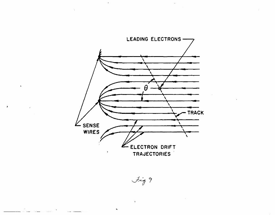
The second major systematic effect is due to the use of leading edge TDC
timing to determine track locations in the chamber. The leading electrons contribut-
ing to the wire signal arrive from different radial positions within a cell, depending
upon the inclination angle of the track relative to the sense wire plane (see Figure 9).
For example, the leading electron from a QO” track will arrive from the center of the
cell, whereas the leading electron from a 10” track will arrive from the edge of the
sense wire cell. This results in an apparent shllt in the r position of the wire, or
equivalently in the z position of the track. Thii effect can be quite large for tracks
at small polar angles. The corrections for this effect depend on the details of the
electric field near the sense wire, diffusion, and ExEt forces. These effects have been
modeled analytically, but better estimates of these corrections are obtained directly
from the data.
Two constraints are useful in determining these corrections. First, tracks
crossing the center high voltage grid of the chamber must be continuous. If track
segments measured in each half of the same module are not aligned, deviations are
assumed to be the result of drift velocity variations and the inclination angle effect
mentioned above. The second constraint ls that the vast majority of tracks originate
from the primsry vertex. Using both of these constraints, the drift velocity and
the polar angle corrections are extracted from fip collision data. This procedure
uses a vertex constrained fit which forces track segments to be continuous across the
central high voltage grid. The drift velocity, the parameterisation of the polar angle
correction, the TDC time offset, and the z position of the vertex are fit for each
event. Only tracks which are isolated in a single octant and found on both sides of
16

the high voltage grid in a single module are used in the fit. Each measured time ti
on a track corresponds to a location y parameterized ss:
G = z, f (V&i - to) + f(e))
where
(1)
z, is the position of the sense wire plane for that particular hit
vd is the driit velocity
ri is the leading edge time from wire i
t. is a global time offset related to the difference between the actual interaction
time and the TDC stop time.
f(e) is the polar angle correction
The “+” ln eq. 1 corresponds to tracks drifting towards smaller values of z,
while *-II refers to tracks drifting in the opposite direction. An event x* is formed
by forcing the vertex z position to be the intercept for all the tracks. By minlling
this x’ with respect to the event vertex, v,+, t. and the parameters for f(e), one can
derive these constants on rm event-by-event basis. Figure 10 shows the wire hits and
the track fits used to determine these constants for a typical event.
The results of these fits yield a measurement of drift velocity for each event.
When averaged over only a few events, a value accurate to < 0.5% can be obtained.
For the majority of runs, the drift velocity is found to be about 4.2 cm/w. The
polar angle correction ls approximated by quadratic splines for dip angles between
30” and 120”, and is assumed linear for lower angles. The asymptotic form of this
17

correction has a slope which ls equal to half the cell spacing. Thii agrees with
expectations based upon purely geometric grounds since for small polar angles the
earliest arriving electrons are those drifting from near the edge of the sense wire cell.
Figure 11 shows a scatterplot of the track mismatch (AZ) as a function of cot(e).
6.2 Pad Reconstruction
The VTPC 4 reconstruction uses pad data and the r-t wire reconstruction informa-
tion to obtain complete three-dimensional tracks. The raw FADC data is converted
into calibrated ADC data by subtracting pedestals and applying electronic gain cor-
rections. The induced charge distribution on a pad row is processed for each FADC
time slice. The 4 position is determined by fitting a Gaussian to the measured
charge distribution. The z is determined from the time address. An approximate
r is determined by the pad row. If this distribution has more than one peak, they
are separated by au iterative process which subtracts contamination from adjacent
peaks. At present, the minimum resolvable 4 ls about one pad spacing (1.4 cm).
The resulting points for each pad row form a group in the z-4 plane. Groups
associated with tracks from the primary vertex are easily recognizable stralght lines
in the 1-4 plane. These lines have small slopes for Pt > 300 MeV/c and are usuahy
well separated in one of the three measured coordinates. This procedure for pattern
recognition ls insensitive to errors in 4 ( - 3” ) and z ( -2 cm ). The lines are then
matched with tracks found in the r-z wire reconstruction and the points associated
with the lines are fit in the t-4 plane. This fit combined with the r-z information
yields complete three dimensional tracks.
18

5.3 dE/dz
The FADC system is also used to measure the dE/dz of charged particles. The
reconstructed r-z track information is used to generate a I window for each wire
FADC channel. The FADC samples within these windows are collected for each
track. After pedestal subtraction, gain corrections, and discarding the largest 35%
of the samples, the mean value of ionization per unit track length is computed.
6 Performance
Figure 12a and 12b show displays of typical 1.8 TeV colliiions observed with the
VTPC system. Figure 12a show a typical event taken with a high Et threshold
calorimetry trigger. Figure 12b shows an event in the VTPC with two pp interactions
in the same crossing.
Several factors contribute to the observed wire resolution. These factors de-
pend upon the angle and position of the track in the chamber. For tracks near !W
(i.e., parallel to the sense wire plane) longitudinal diffusion of electrons dominates the
measured resolution. For tracks highly inclined with respect to the wire plane, diier-
ent effects dominate at different drift distances. Ionization fluctuations dominate the
resolution for short drift distances and transverse diffusion dominates for long drift
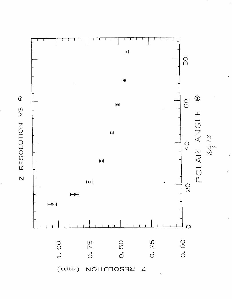
distances. Figure 13 indicates the t resolution as a function of polar angle 8 averaged
over the drift length. For 90” tracks the resolution is 420 pm, rising to 1100 pm at
11”. These data were taken at a luminosity of 2 x 10²’cm-ss-‘. Figure 14 shows
the z resolution squared ss a function of drift distance for 90” tracks. This plot is
expected to be approximately linear because longitudinal diffiion fluctuations scale
19

as the square root of the drii d&stance. The line superimposed on the plot represents
the best fit to the data. The position resolution near the sense wires is about 200
pm, while the resolution for the longest drift times is about 550 pm.
The impact parameter b of tracks with the primary vertex is defined by the
following:
b=(z- zwr..) . sin(e)
Figure 15 shows a histogram of impact parameters of reconstructed wire tracks for
a sample of events taken with a minimum trigger bias. The RMS of the distribution
is about 0.3 em.
Multiple track separation in I is determined primarily by the pulse width of
signals from a single track. At W, the pulse width for a track corresponds to about
0.5 cm of drift length. The effective pulse width grows as cot(e) . W. (where W, is
the wire spacing) for smaller angle tracks.
The chamber precision in 6, is studied using the residuals from the pad data.
For a given FADC sampling, the 4 residual from the fit line in the z-4 plane is
calculated for isolated tracks. The 4 residual is converted into an r-4 residual using
the r information of the track. Figure 16 shows the r-4 residual distribution, which
is fit to a Gaussian with a o of 418 pm. The residual o is about 350 pm per sampling
for a very short drift length (-1-2 cm) and 4OQ450 pm per sampling for a larger
driit length. There are 40 FADC measurements made on a track that extends across
the full 15.25 cm drift region. Because of correlations in successive FADC samplings,
the number of independent measurements is typically about 15. The overall chamber
precision is therefore of order 100 pm.
Over the course of the four month 1987 run, the VTPC modules were operated
20

at nominal voltages for pp integrated luminosity of 70 nb-’ BS well as many days of
stored proton beam. No evidence was observed for aging effects.
7 Space Charge
One of the limiting factors in the VTPC at high luminosity is expected to be buildup
of positive ions in the drift region causing distortions in the drift fields. For our drift
field, the positive ion drift velocity is so low that tens of milliseconds are required to
traverse the drift region. The maximum ion current density that the drift region can
support is estimated in MKS units to be:
J IMI = (1.5)‘E,‘%
where Ed is the electric field strength, p is the positive ion mobility, co is the permit-
tivity of free space, and d is the length of the region. For ion current densities that
are 10% of the maximum, the space charge causes equipotential diiplacements in the
drift direction of about 2 mm. This should cause distortions in the track reconstruc-
tion of the same order of magnitude. It is expected that this current density will be
reached at luminositiw of order 0.5 x 10sscm-‘s-r for our current chamber operating
conditions. At the end of the 1987 CDF run, luminositiw of - 1 x 10aecm-*s-l were
reached.
The effect of drift field distortions is studied by examining systematic shins
of track residuals as a function of luminosity. Tracks which have at least 15 hits in
a single octant are selected for this study. A straight line fit of these tracks is made
using hits only on the middle 15 wires of the chamber. The results of these fits are
extrapolated to both the innermost and outermost wires hit in the chamber. Any
11
drift field distortion appears ss a systematic shift of the residuals of the inner and
outer wires away from zero. At low luminosity, - 1 x 10r’cm%-l the measured
shii are consistent with zero. At luminosities - 1 x 10rscm%-‘, distortions 84
large as 800 pm are observed. The distortion is largest at the innermost wires and
substantially smaller, < 300 pm, for the outermost wires. This variation of distortion
with radius is to be expected because the ion density should be larger closer to the
beam axis. Since the Tevatron operating conditions are usually quite stable over the
period of a typical data run, it is expected that the data can be corrected for these
effects.
For future higher luminosity running, the situation can be improved by raising
the electric field and/or shortening the drift distance ddrilt. Tracking distortions from
positive ion effects should scale roughly as l/d&t. One power of the drift distance
is due to the increased number of positive ions produced at a given luminosity for
a larger active chamber volume. Another power of the drii distance is due to the
magnification of the distortions by a longer lever arm. The third power of drift
distance results from the longer time that the positive ions spend in the drift region.
Shorter versions of the present chambers with higher drift fields are being considered
for the future. Reasonable performance with luminosities of 1031cm-*s-1 should be
attainable.
8 Acknowledgements
The authors wish to thank all members of the CDF collaboration for their help and
advice throughout the course of the project. The success of thii system was the result
12

of the hard work of many individuals. However, the authors wish to especially thank
A. Tollwtrup, E. Erdos, W. Foster, S. Gonzales, A. King, M. Kurisu, R. Paoletti,
A. Pars, D. Tousignant, R. Wagner, and J. Welch for their special efforts on this
project. The authors also wish to thank V. Radeka of B.N.L. for his help in the early
stages of the preamplifier design.
References
[l] F. Abe et al ., The Collider Detector at Fermilab, submitted to NIM.
[2] F. Bedwchi et al ., Design and Construction of the CDF Central Tracking Cham-
ber, submitted to NIM.
[3] M. Atsc et al ., Radial wire Drift Chambers for CDF Forward Tracking, submit-
ted to NIM.
[4] Rohacell foam is a rigid acrylic foam ( density = 0.05) distributed by Cyro
Industries, 25 Executive Blvd, P.O. Box 579, Orange, CT. 06477 Tel. (201)930-
0100.
[5] Kapton is a trademark for a polyimide film manufactured by DuPont de Nemours,
E.I., Co., Wilmington, Del. 19898.
[S] Great Lakes Carbon Co., P.O. Box 810, Rockwood, Term. 37854 Tel. (615)354-
4120.
[7] Gantois, B.P. 307-88105 St.Die Cedex, France. Tel (29)552143.
[8] Polygon Co., P.O. Box 176, Walkerton, IN 46574 Tel (219)5883122.
25

[Q] Methode Development, 7447 W. Wilson, Chicago, IL 60656. Tel (312)867-9600.
[lo] Sheffield Measurement Division, Warner-Swasey/Acoss and Trecker Co., P.O.
Box 1127, Dayton, OH 45401-1127.
[ll] Junkosha Co., Ltd., Hanno Plant, 3-l Ashikariba, Hannoshi, Saitamkken 357
Japan, Tel: 04297-3-2261, Telex: 2954185 JUN HP.
[12] T.k B./Ansiey, 4371 Valley Blvd., Los Angeios, CA 90032.
[13] Hitachi Cable Ltd., Electronic Wire & Cable Design Dep., Hitaka Works, 5-l-l
Hitaka-cho, Hitachi-shi, Ibaraki-ken 31414 Japan.
[14] Fujitsu Microelectronics Ltd., Solid State Department, l&Mori Building, 2-3-13
Torsnomon, Miiato-ku, Tokyo, Japan.
[15] R. J. Yarema et al . A Surface Mount Amplifier-Shaper-Discriminator and
Preamplifier for the Fermilab CDF Tracking Chambers, IEEE Trans. =(1986)933.
[16] LeCroy Research Systems Corp., 700 S. Main Street, Spring Valley, New York
10977.
[17] H. Brafman et al ., IEEE Trans. N&,3.2(1985)336.
[18] R. A. Boie et al ., IEEE Trans. ~(1981)603.
[lQ] Ma. et al MIT Technical reports 129 and 130 (1982).
24
Dimenaionr:
End Caps:
Field Cage:
Magnetic Field:
Drift Field: GaS:
V&ages:
Electronics:
Tab: # mod&a Module length
Modules spacing
Max. active radios: Min. active radios: Drii Length:
Sense wii:
Field Wi:
Cathode Pads:
Resistive ink: Material:
Electrodes
Central grid
Cathode-grid
Lw &dd (-4 &if, Argon-Ethme Drift velocity
Cathode Field Shaping
Central grid Sense wire
# wii channels
i Pad channels # dE/dz channels
L: VTPC Specilkationa 8 s5.s cm 55.94 cm 11 em 7cm 1525 cm 24 /octmt
Ie 1
,
,
I
I
6.338 mm spacing 15 jnn gold-plated tungsten. a4 /octant
53 pm copp.+feryuiom
a4 p.sds/octant, in s ro”S
4.12 cm in I by e 1.4 em in r-4
10 Mn/aqnm
Ka~pto~~/RohaceU foam laminate epoxy/graphite-foam support frame
5.175 mm ov&.pping strip on 2.38 mm centers
* acreen 50 pm rim on loa, /ml centers
I SIxem 50 pm wired on 500 &ml center9
1.5 Tesls
c 1%&i.+ 150 v/cm
so/so at 1 atm.
42 pm/n8 -1.5 LV -1.6 kV -6.4 kV I
25

Figure Captions
l Figure 1. Cross section through l/4 of the CDF central detector showing the
location of the VTPC system. Drift spaces marked with an * are instrumented
for pad and dE/d.z readout with FADCs.
l Figure 3. An isometric view of two VTPC modules. They are rotated in 4 by
11.3” with respect to each other.
l Figure 3. Construction details of the VTPC proportional chamber region.
. Figure 4. Four VTPC modules in their service position during installation. The
preamplifier cards and ribbon coax cables are in place on the modules. The
CTC endplate is seen in the background.
l Figure 5. Material traversed versus polar angle.The dotted lime indicates mate-
rial traversed before entering the active volume of the VTPC. The dot-dash line
indicates the total amount of material crossed by a particle as it exits the VTPC
system. The solid line and arrows indicate the average total material traversed
before entering the active volume of the CTC or FTC.
l Figure 6. Simplified schematic of VTPC wire electronics.
l Figure 7. Simplified schematic of VTPC pad electronics.
l Figure 8. Distribution of event vertices along the beam axis for a typical CDF
l Figure 9. Leading electron effect due to track polar angle 8. The first electrons
arriving at the sense wire come from different radial regions in the cell and follow
different drii trajcetories, depending on track polar angle 8.
26

. Figure 10. The r-s projection of a typical event used in determining the VTPC
reconstruction constants. Shown are the track fits constrained to a common
vertex, and the wire hits used in these fits.
. Figure 11. Scatterplot of the mismatch in s for tracks crossing the center grid
as a function of cotan(
l Figure 12. Event displays showing an r-z projection of the VTPC wire hits. a)
A typical large Et triggered event. b) Two 1.8 TeV pp collisions occuring in the
same Tevatron bunch crossing. Note that the vertical scale in these displays is
magnified by a factor of four relative to the horizontal scale.
. Figure 13. z resolution per wire averaged over drift distance as a function of
track angle 8.
. Figure 14. s resolution squared per wire for 90” tracks ss a function of drift
distance.
. Figure 15. Distribution of impact parameters for all tracks. The sigma of the
distribution is 0.3 cm.
l Figure 16. Distribution of r-4 residuals from pad data. An r-4 residual is
calculated for isolated tracks for each FADC sampling. The o of the distribution
ia 418 pm.
27

SUPLRCONDUCTINQ COIL
CENTRAL TRACKINQ CHAMBER (AXIAL WIRE DRIFT CHAMBER)
B-- 1.5 1 VERTEX T.P.C.
CABLINS
E.N. SHOWER COUNTER
/ SIONAL CABLES
TO A.s.R f /’ ,‘30’
- r,r
I F.T.C. COVERAOE
I
--Scm DIA.Bo.BEAN PIPE
SENSE WIRES SENSE WIRE READ-OUT
PAD RE :AD-OUT 7
CARBON
CATHODE PADS
x /
CARBON FIBER OCTOGON
CENTER HU GRID
RADIAL BOARD
FIBER OCTDGDN
\,\\ \ INNER FIELD CAGE
OUTER FIELD CAGE
i&TlVE DIVIDER
vTi?C. MODULES
CATHODE GRID
FIELD SHAPING ELECTRODES (Cr-KAPTON-CU.)
SEE OUTER FIELD CAGE DETAIL
,-FOAM CORE
LGRIO I
OUTER FIELD CAGE DETAIL
I - FIELD SHAPING WIRE
2- SENSE WIRE
3- MULTI (3) LAYERED RADIAL BOARD
4- FIELD SHAPING ELECTRODES S- WIRE PRE-AMP.
G- OUTER FIELD CAGE I- MINI.- COAX. CABLE (25)
G- CATHODE GRID 9- EPOXY/GRAPHITE- FOAM FRAME
IO- RESISTIVE INK CATHODE
II- CATHODE PAD l2- PAD READ-OUT
IS- PAD PRE-AMP.

I . I :- ;+
I ;
I i i
I :_ .
I, . I :, . I i’
I I’
Y%
I I
SOLENOID I ENDWALL +COUNTlNG ROD”
PREAMPLIFIER CARD
CROSSTLLI NLTIWn FUN,”
I 1 I I I I
I
I I
-10 MITERS
-
JurMoswA YMICOAX, mmm ClllLE
ILS cnn., 1 , I 1 I I I I
AMPLIFIER-SHAPER-DISCR. CARD
I’
I I I
I 1 I
1 /
-61 Y&S
P---W- -
T~8/AI(SLLI FLAT CAOLL It4 cnrr.,
, I
I I
E CROY TD.C~lS79l
1 36 CHAHnEL PER
FflSTB”J MOOULE

SOLENOID i
PREAMPLIFIER CARD
ii+-$
-< CALImLT,M( I. cnr”Pltls /CARD
-10 I
R -
J”I MI!
R
,I
1
I
I
iv I I
I
-r- WO! mco 11mc CAEi !5 Cl
I I I I
I I I I I I I I
ENDWALL I
COUNTINO ROOM
PA0 AMPLIFIER-SHAPER CAR0
CILIB. POLL- SlO”lL *L”o
FLTE”
ti
7
I “LUUWW 1ESDTOR
I I I I 1 I
I I 1 I
-O’ YLRS I
FA.0.C. MODULE
VIDEO AYPLIFIE”
4 lT.OL
l----b
OA”,,ll~ IWTEO”bVM 8OP
t
A
-_------ ----- ---, MIACH
:, ,“ILLOI TWISTL 0 Mm 8LE Y I., I I I I
I I
“.E,A. ,“A”,- “.E,A. ,“A”,- ,orw ,orw COuo”CT.*Ct COuo”CT.*Ct rlDe rlDe AYPLCIE” AYPLCIE”
@ @
CIA CIA i i
mm, y mm, y
P P
5cl& 5cl& PEDESTAL PEDESTAL
1 T ,flASELl”E ,flASELl”E RE’IIWIERI RE’IIWIERI
:X9
- - -
I”1 AX. II L m,
I I
1 48 CHl..EL$ICAR0
ii (2.
FASTSUS COMPACTION MODULE
I
0 0
: 0 N
0
: 7
0
: r
0
si
0 d
0
: I
0 d 0 7 I
0
0 ’ 0
d ?1r,
I- Oi
SlN3h3 JO H38WnN
LEADING ELECTRONS
7 - .-
\ /
\ / \ \ /
c ELECTRON DRIFT TRAJECTORIES
,

_. . . _ . . . _.._._.........._____.......~..~.
- \
. . . . . ;‘_..... 1, y . . -. . . . - . . . ..-... _.-...
-. *\.
- \ ‘,.
.._
_..
. .
. .
.,
.,
4’ l
. ..-..............~........t................ .4
f .4
*
“““‘~..‘.‘~‘.~“‘....... . . . . . . . . . . . . . . .
. . . . . . .
_.._..__.__~_.._.___._ . . .._.__._..____...
_..__._.._.......-~....-...-
*..
‘\ *~ \
‘1 -- \; . __..._.. . . . . . . . . ._......._.
\
__.____.......... . . . _.........
.

.
I I I I I 0 0 0 0 0
d r, c-4 r d
P3) z v
i
0 4
0 d-3 Gi
G I 0 ?
0 b
cu ,
I
0
ti I
0 u, I

t -4 .,?..tZ.- ..____.._............ ‘;‘i’T’ _......
. I.l.ill.@‘-- 1 . . . . ..--- L - wlrr
._. ~~~~~~..
e. .f!:.iZc
,:i:. ‘br,:‘~;‘ll;!(q i”-’ ~.:..~g!,~l.~: t -9. . . +*I!. .,
:. . . . . . *.;a. I *‘Y-&X ..-..
1 I:..
. -. =r -: -::.. -.
.,.C
.- i-_.t. +...... i
. -4. a *itI I.
::-y:. “.y;: -
.‘.. ;i’ +:;r’ *-
8; . v. ;:-, . * 1 . . . . : -t .i’C, .,-
ytiJ::i;:..-i:=;T 1
_.__ :..::.zif& __. r&i: j ]!.~f:--::*$::;; 1

r-
11 ?F,p$4 3 iv . . . . . +$h;. . :..I;-:.
2:. -.-f...... I:+-- *.. t-t. ‘a.-* 1. !. -9
=yy,~:~p+ * ‘3 ,___ j:...~:.!..rrr,~~+.. -xi- ’ .%J-..*’
ek$&$!j:-g$
__... p?$g *g .tSL
% :.y,:,;+g!i;~,. *- * g!ip--.*:-:-~.J$ti
...e.pz2F . . ::$;y!
;rs-‘--.w u $-q-.*-:wy~-~~’
. *Jf!h ,... +E .._ ‘;q#$$g$
~~g!~.~*~~” . ..V
,..-.s(~; 1 ,&l.y&!{
-.-.--~;~fi~; ::-a:,& :+3-:+-i q+‘.;&y .?..I-+
I ,qii&:,&L .- 1*&f&.‘;,: 9:’ *. \~I::.+ LI* 2: :’
,....
I
I ._..
,....
i
.._.
_.
I
0
Y
6 F 3 -I F: W K
N
, I I I 1 I I I I I I I I I I I I I I
N. s E if? 2 g A 6 6 6 6 Q-J--> NOllnlOS3a z
0 W
d
Z Q CL 4 0 CL

t
g
u-l
>
0
I z E I-- > 2 u-l i!i N
E
0 II) 0 m 0 Ln 0 u-l nl N .-4 4 0 0
d d d d 6 6 d
( ww) a3avnos r;lounlos3a z
t iY n

1 I I 1
f ‘;t
I
C
I I I I
0 0 0 0 0
s d d d 0 g 0
co u) e cu
SN3Vlll JO kJ38WnN

22 b
z -sz % E 10 2 2 G 0% -%a ‘2