- gntechemrl.gntech.ac.kr/publication/sci9.pdf · vol. 24 † no ... (mw)-scale piezoelectric...
TRANSCRIPT

www.afm-journal.de
Vol. 24 • No. 18 • May 14 • 2014
ADFM_24_18_cover.indd 1ADFM_24_18_cover.indd 1 16/04/14 4:34 PM16/04/14 4:34 PM
www.afm-journal.de
FULL
PAPER
© 2014 WILEY-VCH Verlag GmbH & Co. KGaA, Weinheim2620
www.MaterialsViews.com
wileyonlinelibrary.com
1. Introduction
Energy harvesting using mechanical energy sources (e.g., human walking, transportation movement, and even sound waves) is a promising candidate for energy generation with improved accessibility and eco-compatibility. [ 1–3 ] Since the fi rst nanogenerators were demonstrated for direct energy conver-sion from mechanical motion to electrical power, [ 4 ] the develop-ment of milliwatt (mW)-scale piezoelectric nanogenerator has been attempted to establish wireless communication-sensor networks and self-powered fl exible electronics in biological and environmental monitoring systems. [ 1,5–7 ] Recently, a fl exible nanocomposite generator (NCG), using perovskite piezoelectric
BaTiO 3 nanoparticles (BTO NPs) and gra-phitic carbon nanomaterials, was reported by our group to provide cost-effective and fl exible energy harvesting systems for self-powered nano/micro-devices. [ 8 ] However, the previous NCG device had critical drawbacks to be resolved such as low piezoelectric properties of BTO NPs and aggregation of graphitic carbon nanomaterials.
Among the various lead-free perovs-kite materials with high piezoelectricity, such as Ba(Zr, Ti)O 3 (BZT), [ 9 ] (Bi, Nd)Ti 3 O 12 , [ 10 ] SrBi 2 Ta 2 O 9 , [ 11 ] and (K, Na)NbO 3 (KNN), [ 12 ] KNN-based alkaline niobate is the most attractive lead-free piezoelectric materials due to its remarkable piezo-electric properties, biocompatibility, high Curie temperature, and large electrome-chanical coupling factor. [ 13,14 ] Especially, KNN-based materials modifi ed by doping elements can have noteworthy piezoelec-
tric coeffi cients (d ij ) (>300 pC N −1 ), [ 13,15 ] compared to BTO, [ 16 ] KNbO 3 , [ 17 ] NaNbO 3 , [ 18 ] or pure KNN [ 19,20 ] (<100 pC N −1 ). In par-ticular, a specifi c alkaline niobate-based materials of outstanding piezoelectricity (d 33 ≈ 310 pC N −1 ) was reported with the nom-inal composition of 0.942(K 0.480 Na 0.535 )NbO 3 -0.058LiNbO 3 (KNLN). [ 21,22 ] In addition to piezoelectric material properties, to achieve a high-output nanocomposite generator, good dispersity of piezoelectric particles is also very important for well-distributed piezopotential within an active energy harvesting composite layer. For uniform dispersion, metal nanowires and nanorods are considered more suitable for nanocomposite systems than the previous carbon-based nanofi llers of BTO-based NCG, due to the weak van der Waals self-interactions of metal nanomaterials. [ 23 ]
Herein, we demonstrate a high-performance, lead-free NCG device using the intrinsically excellent piezoelectric KNLN par-ticles and well-dispersed copper nanorods (Cu NRs). The KNLN particles as power generation sources and Cu NRs as energy enhancers are embedded in a polydimethylsiloxane (PDMS) elastomeric matrix to construct a piezoelectric nanocomposite (p-NC). The roles of the Cu NRs in the p-NC are dispersing, reinforcing, and conducting agents for the high-output NCG device. The spin-casted p-NC layer is placed between two dissimilar indium tin oxide (ITO)-deposited polyethylene terephthalate (PET) fl exible substrates. During periodical
Large-Area and Flexible Lead-Free Nanocomposite Generator Using Alkaline Niobate Particles and Metal Nanorod Filler
Chang Kyu Jeong , Kwi-Il Park , Jungho Ryu , Geon-Tae Hwang , and Keon Jae Lee *
The lead-free nanocomposite generator device for high-output energy har-vesting using piezoelectric alkaline niobate-based particles (KNLN) and copper (Cu) nanorods fi ller is reported. To produce the piezoelectric nanocomposite (p-NC), lead-free KNLN particles synthesized using a solid-state method and the Cu nanorods are distributed in a polydimethylsiloxane (PDMS) matrix. The lead-free fl exible nanocomposite generator (NCG) made by a simple spin-casting method successfully converts mechanical energy to electricity up to 12 V and 1.2 µA. These are higher than previously reported outputs from other lead-free and composite-based nanogenerators. The harvested energy is utilized to directly turn on white light emitting diodes (LEDs) without external circuits and to operate a complex circuital liquid crystal display (LCD). A large-area NCG device (30 cm × 30 cm) is also fabricated using the bar-coating method to obtain maximum output up to 140 V and 8 µA (≈0.5 mW). This NCG technology has substantial advantages as a simple, cost-effective, scalable, and high-throughput approach for practical fl exible electronics, bio-eco-compatible self-powered systems, and body sensor networks (BSN).
DOI: 10.1002/adfm.201303484
C. K. Jeong, K.-I. Park, G.-T. Hwang, Prof. K. J. Lee Department of Materials Science and Engineering Korea Advanced Institute of Science and Technology (KAIST) 291 Daehak-ro , Yuseong-gu Daejeon , 305–701 , Republic of Korea E-mail: [email protected] Dr. J. Ryu Functional Ceramics Group Korea Institute of Materials Science (KIMS) 797 Changwondaero , Seongsan-gu, Changwon , Gyeongnam , 642–831 , Republic of Korea
Adv. Funct. Mater. 2014, 24, 2620–2629

FULL P
APER
2621
www.afm-journal.dewww.MaterialsViews.com
wileyonlinelibrary.com© 2014 WILEY-VCH Verlag GmbH & Co. KGaA, Weinheim
2. Results and Discussion
Figure 1 a presents the schematic of the NCG structure with KNLN particles and Cu NRs, which construct a well-distributed p-NC layer in the device. The two ITO electrodes on the fl ex-ible PET substrate act as a current collector in the NCG device. The pure PDMS dielectric layers are used to prevent electrical breakdown during the high voltage poling process and extreme mechanical deformation. A fl exible p-NC fi lm can be com-pletely attached to a curved surface, as shown in Figure 1 b,
bending deformation, the KNLN-based fl exible NCG device (3 cm × 3 cm) produced maximum electrical signals of ≈12 V and ≈1.2 µA, which are four times higher than those of a pre-vious lead-free BTO/carbon nanotube (CNT)-based NCG device. The electrical energy is utilized to directly turn on white light emitting diodes (LEDs) without external circuits and to operate a complex circuital liquid crystal display (LCD). Furthermore, a large-area NCG device (30 cm × 30 cm) by the bar-coating method can convert the biomechanical energy to sub-mW level power (140 V and 8 µA).
Figure 1. a) Schematic of an NCG device using KNLN particles and Cu NRs. b) Photograph of the fl exible p-NC layer attached to a rolled paper. The inset shows the fi nal NCG device bent by fi ngers. c) Cross-sectional SEM image of a bent KNLN-based NCG. d) Schematics showing the power generation mechanism of the NCG device. In the bending state, the current fl ow is generated from top to the bottom electrode due to the positive piezoelectric potential induced on the top side. In the unbending state, the accumulated charges return to the original state due to piezopotential vanishment which causes output signals in the opposite direction. e) Simulation result of generated piezopotential distribution inside a p-NC layer of well-dispersed KNLN particles, when a tensile strain of 0.33% is applied by bending.
Adv. Funct. Mater. 2014, 24, 2620–2629
FULL
PAPER
2622
www.afm-journal.dewww.MaterialsViews.com
wileyonlinelibrary.com © 2014 WILEY-VCH Verlag GmbH & Co. KGaA, Weinheim
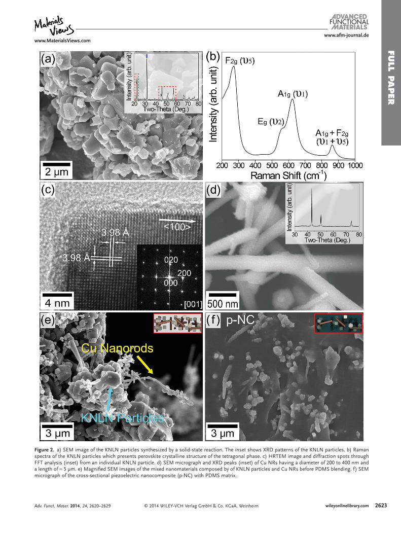
the high-back doublets at 22°, 46°, 51°, and 57° (see Figure S1 in the Supporting Information for the magnifi ed XRD pattern of the red-dotted border). In the Raman spectrum of KNLN par-ticles (Figure 2 b), the main vibration modes associated with the perovskite crystal structure are shown. The A 1g ( υ 1 ) and F 2g ( υ 5 ) Raman modes, in particular, are strongly detected as well-known phenomena in KNN-based materials. [ 15 ] Moreover, the weak E g ( υ 2 ) shoulder at 560 cm −1 and the small mound in the 400 to 500 cm −1 region prove the tetragonal phase of the KNLN par-ticles. [ 31 ] These XRD and Raman spectroscopy results indicate that the synthesized KNLN particles have a perovskite crystalline structure and ferroelectric tetragonal phase. The crystal struc-ture of the KNLN particles is also investigated by high resolu-tion transmission electron microscopy (HRTEM), as shown in Figure 2 c. The diffraction pattern through the fast-Fourier trans-form (FFT) analysis indicates a single crystal structure (inset of Figure 2 c). The interplanar distance displayed in the HRTEM image corresponds to the (010) and (100) crystal planes; which have lattice parameters of a = b in tetragonal symmetry. [ 32 ] The Cu NRs (Sky Spring Nanomaterials, Inc.), which have a dia-meter of 200 to 400 nm and a length of ≈5 µm (Figure 2 d), show XRD patterns of good crystallinity with very few tenorite (CuO) peaks of (inset of Figure 2 d). Figure 2 e displays an SEM micro-graph of mixed nanomaterials with KNLN particles and Cu NRs. A magnifi ed cross-sectional SEM image of the p-NC (Figure 2 f) also shows that the KNLN particles and Cu NRs are well-dis-persed in the elastomeric matrix. These images verify that good dispersity of the KNLN particles and Cu NRs is maintained before and after mixing with the PDMS elastomeric matrix.
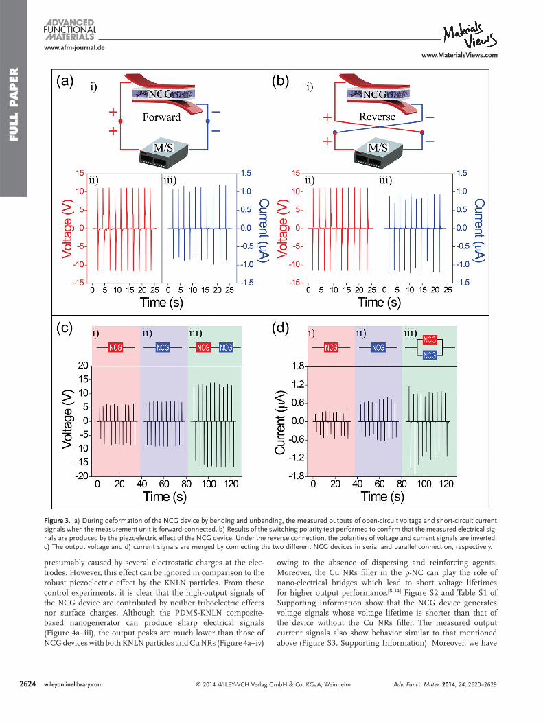
To measure the electrical signals from the NCG device, a source-meter (Keithley 2612A), a linear motor, and a Faraday cage are used in this work. During the mechanical bending deformation, the uniform voltage and current outputs are gen-erated from the lead-free KNN-based NCG device ( Figure 3 a,b). The open-circuit voltage and short-circuit current by the NCG device are about 12 V and 1.2 µA, respectively. These output signals are the highest output recorded among those of previ-ously reported fl exible and lead-free composite-based nanogen-erators. [ 8,17,18,33–35 ] To confi rm the measured electrical signals from piezoelectric outputs of the NCG device, a switching polarity test has been performed. When the measurement unit has a forward connection with the KNLN-based NCG device (Figure 3 a–i), positive pulses are measured during the bending motions (Figure 3 a–ii,a–iii). Under the reverse connection (Figure 3 b–i), on the other hand, negative peaks are gener-ated in the bending states of NCG device (Figure 3 b–ii,b–iii). Furthermore, we have conducted a linear superposition test which shows the merged output voltage (Figure 3 c) and cur-rent (Figure 3 d) by connecting the two different NCG devices in series and in parallel, respectively. From these results, the generated signals can be verifi ed as electrical outputs by the mechanically stressed KNLN-based p-NC in the NCG devices.
Figure 4 a presents the output voltages generated from the devices fabricated using only a PDMS layer (i), a Cu NRs-PDMS composite (ii), a composite with only KNLN particles (iii), and an NCG device (iv). As shown in Figure 4 a–i,a–ii, there is no reliable signal from devices containing only a pure PDMS layer, or from Cu NRs embedded in a PDMS layer. Some low electrical signals from these two devices without KNLN particles are
and is placed between the different top and bottom ITO-depos-ited PET substrates for the bendable NCG device (inset of Figure 1 b). Figure 1 c shows the cross-sectional SEM image of a bent KNLN-based NCG device made of a p-NC (thick-ness in 250 µm) which is sandwiched between the two fl exible substrates. Despite the mechanical deformation, there is no separation of the p-NC layer and plastic substrates owing to the inherent stickiness of the PDMS. The process of energy gen-eration from the NCG device is illustrated in Figure 1 d, which shows that KNLN particles harvest external mechanical energy to make electrical potential. Typically, the perovskite KNN-based piezoceramics have orthorhombic or tetragonal crystalline sym-metry, with monoclinic subcell structure at around Curie tem-perature. [ 24 ] When the NCG is subject to external bending force, piezoelectric potential is generated between the two electrodes due to the mechanical stress induced in the aligned dipoles of the embedded KNLN particles. These positive and negative piezopotentials make an instantaneous built-in potential in the external circuit, which drives the current fl ow (top panel of Figure 1 d). During the subsequently unbending of the NCG device, the mechanical stress and piezoelectric potential disap-pear, which can cause reverse electrical signals (bottom panel of Figure 1 d). A simulation for the induced piezopotential in mechanically stressed KNLN-based NCG is also performed via a fi nite element method (FEM) with six KNLN particles well-dispersed in a PDMS elastomeric matrix, which is conducted by using COMSOL multiphysics software, as described in Figure 1 e. The p-NC layer in the NCG suffers tensile stress during bending deformation because the p-NC is placed above the mechanically neutral region. Differences in the piezoelec-tric potential are illustrated by color code, when a tensile strain of 0.33% is applied to the p-NC layer along the x-axis. The sim-ulated piezopotential distribution in the KNLN-based p-NC is higher than that of BTO NPs embedded p-NC, due to the high electromechanical coupling factor ( k ) of KNLN caused by its low permittivity (dielectric constant, ε ) and large d 33 . The value of k indicates the effectiveness of conversion between mechan-ical and electrical energy, and can be expressed as follow
k Y g d Y
dij ij
ij
T2
2
ε= × × = ×
(1)
where Y , g ij , and ε T are the Young’s modulus, piezoelectric voltage constant, and permittivity at constant strain. [ 25,26 ] The physical properties of KNLN established in previous theoretical reports are applied in this simulation. [ 19,21,27–30 ] Based on the results from this FEM-based simulation, the KNLN particles-based NCG device can be expected to generate high electrical outputs from mechanical stress, compared to previous BTO-based NCG. [ 8 ]
The highly piezoelectric KNLN particles used in this study are fabricated by the solid-state synthesis method (see Experi-mental Section). Scanning electron microscopy (SEM), X-ray diffraction (XRD), and Raman spectroscopy are utilized to char-acterize the KNLN particles. Figure 2 a is an SEM image of the KNLN particles which have polydisperse angulated shapes of 1 to 3 µm. The XRD patterns of the as-synthesized KNLN (inset of Figure 2 a) correspond well to those of general perovskite KNN-based materials. [ 24 ] The XRD peaks indicate the tetragonal phase of KNLN due to the near-singlet at 32° (blue arrow) and
Adv. Funct. Mater. 2014, 24, 2620–2629
FULL P
APER
2623
www.afm-journal.dewww.MaterialsViews.com
wileyonlinelibrary.com© 2014 WILEY-VCH Verlag GmbH & Co. KGaA, Weinheim
Figure 2. a) SEM image of the KNLN particles synthesized by a solid-state reaction. The inset shows XRD patterns of the KNLN particles. b) Raman spectra of the KNLN particles which presents perovskite crystalline structure of the tetragonal phase. c) HRTEM image and diffraction spots through FFT analysis (inset) from an individual KNLN particle. d) SEM micrograph and XRD peaks (inset) of Cu NRs having a diameter of 200 to 400 nm and a length of ≈ 5 µm. e) Magnifi ed SEM images of the mixed nanomaterials composed by of KNLN particles and Cu NRs before PDMS blending. f) SEM micrograph of the cross-sectional piezoelectric nanocomposite (p-NC) with PDMS matrix.
Adv. Funct. Mater. 2014, 24, 2620–2629
FULL
PAPER
2624
www.afm-journal.dewww.MaterialsViews.com
wileyonlinelibrary.com © 2014 WILEY-VCH Verlag GmbH & Co. KGaA, Weinheim
owing to the absence of dispersing and reinforcing agents. Moreover, the Cu NRs fi ller in the p-NC can play the role of nano-electrical bridges which lead to short voltage lifetimes for higher output performance. [ 8,34 ] Figure S2 and Table S1 of Supporting Information show that the NCG device generates voltage signals whose voltage lifetime is shorter than that of the device without the Cu NRs fi ller. The measured output current signals also show behavior similar to that mentioned above (Figure S3, Supporting Information). Moreover, we have
presumably caused by several electrostatic charges at the elec-trodes. However, this effect can be ignored in comparison to the robust piezoelectric effect by the KNLN particles. From these control experiments, it is clear that the high-output signals of the NCG device are contributed by neither triboelectric effects nor surface charges. Although the PDMS-KNLN composite-based nanogenerator can produce sharp electrical signals (Figure 4 a−iii), the output peaks are much lower than those of NCG devices with both KNLN particles and Cu NRs (Figure 4 a−iv)
Figure 3. a) During deformation of the NCG device by bending and unbending, the measured outputs of open-circuit voltage and short-circuit current signals when the measurement unit is forward-connected. b) Results of the switching polarity test performed to confi rm that the measured electrical sig-nals are produced by the piezoelectric effect of the NCG device. Under the reverse connection, the polarities of voltage and current signals are inverted. c) The output voltage and d) current signals are merged by connecting the two different NCG devices in serial and parallel connection, respectively.
Adv. Funct. Mater. 2014, 24, 2620–2629

FULL P
APER
2625
www.afm-journal.dewww.MaterialsViews.com
wileyonlinelibrary.com© 2014 WILEY-VCH Verlag GmbH & Co. KGaA, Weinheim
When the Cu NRs amount is above 1 g, the electrical output signals decline with increasing concentration of Cu NRs, due to leakage charge fl ows within the p-NC caused by weakened insulation of the polymeric matrix. When the amount of KNLN particles is varied (Figure 4 c), the generated outputs of NCG devices increase initially with the weight of KNLN particles (fi xed Cu NRs weight of 1g) due to the increment of piezoelec-tric particle density in the p-NC. Moreover, Maxwell-Wagner-Sillars polarization, which introduces a dramatic change of the overall dielectric constant in composites, [ 39,40 ] can rise with increasing amount of KNLN particles. This leads to extensive polarization which results in high output signals. However, an excessive amount of KNLN particles (above 2 g) in the p-NC lowers the electrical outputs from NCG devices because of the degraded electromechanical coupling effect resulting from an overly-high dielectric constant of the entire p-NC, as expressed by Equation 1 . In addition, the large quantity of piezoceramic elements in a composite also can yield the electrical break-down, resulting in low generated outputs. [ 35 ]
The poling process is necessary to align the piezoelectric dipoles in the KNLN particles along an identical direction to
measured electrical outputs from a KNLN-based NCG device with multi-walled CNTs (MW-CNTs), which have roles similar to those of Cu NRs in an NCG device (Figure S4, Supporting Information). The signals generated from an NCG device using MW-CNTs are lower than those of the NCG device with Cu NRs fi ller because MW-CNTs are easily aggregated and bundled compared to Cu NRs, as shown in Figure S5 (Supporting Infor-mation). It is presumably due to the large van der Waals forces of MW-CNTs caused by π–π staking interactions [ 36–38 ] that can induce aggregation. The NCG device using Cu nanoparticles (Cu NPs) as nanofi llers generates low output signals since the low aspect ratio cannot contribute the dispersity of p-NC, as shown in Figure S6 (Supporting Information).
To determine an optimal composition of the p-NC for effec-tive energy harvesting, NCG devices with various mixture ratios are fabricated with different amounts of KNLN particles and Cu NRs (in 10 g of PDMS matrix). As shown in Figure 4 b, the output voltage and current signals from deformed NCG devices rise with increasing amounts of Cu NRs, up to 1g at the fi xed weight (2 g) of KNLN particles, since the Cu NRs fi ller func-tions as the dispersing, reinforcing, and conducting agent.
Figure 4. a) Output voltage generated from the devices fabricated using only a PDMS layer (i), a Cu NRs-PDMS composite (ii), a composite with only KNLN particles (iii), and an NCG device (iv). b) Variation of output voltage and current produced from NCG devices with the different weights of Cu NRs at the fi xed weight of KNLN particles. c) Generated output signals of NCG devices with various weights of KNLN particles at the fi xed amount of Cu NRs.
Adv. Funct. Mater. 2014, 24, 2620–2629
FULL
PAPER
2626
www.afm-journal.dewww.MaterialsViews.com
wileyonlinelibrary.com © 2014 WILEY-VCH Verlag GmbH & Co. KGaA, Weinheim
device, at different frequencies and strain rates, are also meas-ured (Figure S7, Supporting Information).
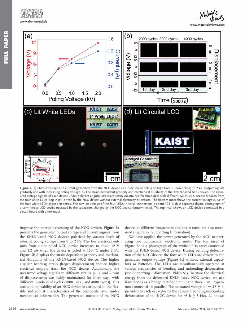
We have applied the power generated by the NCG to oper-ating two commercial electronic units. The top inset of Figure 5 c is a photograph of the white LEDs array connected with the KNLN-based NCG device. During bending deforma-tion of the NCG device, the four white LEDs are driven by the generated output voltage (Figure 5 c) without external capaci-tors or batteries. The LEDs are simultaneously operated at various frequencies of bending and unbending deformation (see Supporting Information, Video S1). To store the electrical energy from the deformed KNLN-based NCG device, we use four diodes as a bridge rectifi er circuit, and three 1 mF capaci-tors connected in parallel. The saturated voltage of ≈4.18 V is provided to each capacitor by the repeated bending/unbending deformation of the NCG device for ≈5 h (4.5 Hz). As shown
improve the energy harvesting of the NCG devices. Figure 5 a presents the generated output voltage and current signals from the KNLN-based NCG devices polarized by various levels of external poling voltage from 0 to 2 kV. The low electrical out-puts from a non-poled NCG device increases to about 12 V and 1.2 µA when the device is poled at 150 °C under 2 kV. Figure 5 b displays the strain-dependent property and mechan-ical durability of the KNLN-based NCG device. The higher angular bending strain (larger displacement) induce higher electrical outputs from the NCG device. Additionally, the measured voltage signals in different strains (2, 3, and 5 mm of displacement) are stably maintained for three days with different numbers of cycles (2000, 3000, and 4000 cycles). This outstanding stability of an NCG device is attributed to the fl ex-ible and robust characteristics of the composite layer under mechanical deformation. The generated outputs of the NCG
Figure 5. a) Output voltage and current generated from the NCG device as a function of poling voltage from 0 (non-poling) to 2 kV. Output signals gradually rise with increasing poling voltage. b) The strain-dependent property and mechanical durability of the KNLN-based NCG device. The meas-ured voltage signals of each device under different angular strain are stably maintained for three days with different cycles. c) A snapshot taken from the four white LEDs (top inset) driven by the NCG device without external electricity or circuits. The bottom inset shows the current-voltage curve of the four white LEDs aligned in series. The turn-on voltage of the four LEDs in serial connection is about 10.5 V. d) A captured digital photograph of a commercial LCD device operated by the capacitors charged by the NCG device (bottom inset). The top inset shows an LCD device connected in a circuit board with a text mask.
Adv. Funct. Mater. 2014, 24, 2620–2629
FULL P
APER
2627
www.afm-journal.dewww.MaterialsViews.com
wileyonlinelibrary.com© 2014 WILEY-VCH Verlag GmbH & Co. KGaA, Weinheim
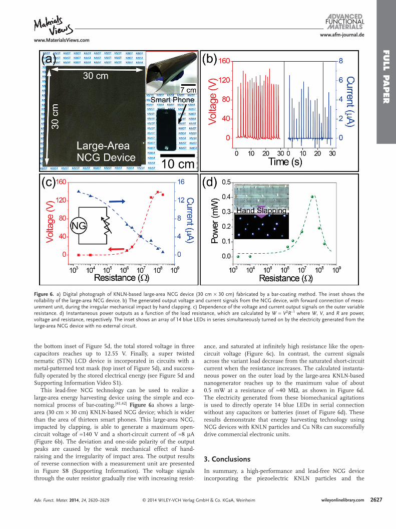
ance, and saturated at infi nitely high resistance like the open-circuit voltage (Figure 6 c). In contrast, the current signals across the variant load decrease from the saturated short-circuit current when the resistance increases. The calculated instanta-neous power on the outer load by the large-area KNLN-based nanogenerator reaches up to the maximum value of about 0.5 mW at a resistance of ≈40 M Ω , as shown in Figure 6 d. The electricity generated from these biomechanical agitations is used to directly operate 14 blue LEDs in serial connection without any capacitors or batteries (inset of Figure 6 d). These results demonstrate that energy harvesting technology using NCG devices with KNLN particles and Cu NRs can successfully drive commercial electronic units.
3. Conclusions
In summary, a high-performance and lead-free NCG device incorporating the piezoelectric KNLN particles and the
the bottom inset of Figure 5 d, the total stored voltage in three capacitors reaches up to 12.55 V. Finally, a super twisted nematic (STN) LCD device is incorporated in circuits with a metal-patterned text mask (top inset of Figure 5 d), and success-fully operated by the stored electrical energy (see Figure 5 d and Supporting Information Video S1).
This lead-free NCG technology can be used to realize a large-area energy harvesting device using the simple and eco-nomical process of bar-coating. [ 41,42 ] Figure 6 a shows a large-area (30 cm × 30 cm) KNLN-based NCG device; which is wider than the area of thirteen smart phones. This large-area NCG, impacted by clapping, is able to generate a maximum open-circuit voltage of ≈140 V and a short-circuit current of ≈8 µA (Figure 6 b). The deviation and one-side polarity of the output peaks are caused by the weak mechanical effect of hand-raising and the irregularity of impact area. The output results of reverse connection with a measurement unit are presented in Figure S8 (Supporting Information). The voltage signals through the outer resistor gradually rise with increasing resist-
Figure 6. a) Digital photograph of KNLN-based large-area NCG device (30 cm × 30 cm) fabricated by a bar-coating method. The inset shows the rollability of the large-area NCG device. b) The generated output voltage and current signals from the NCG device, with forward connection of meas-urement unit, during the irregular mechanical impact by hand clapping. c) Dependence of the voltage and current output signals on the outer variable resistance. d) Instantaneous power outputs as a function of the load resistance, which are calculated by W = V 2 R −1 where W , V , and R are power, voltage and resistance, respectively. The inset shows an array of 14 blue LEDs in series simultaneously turned on by the electricity generated from the large-area NCG device with no external circuit.
Adv. Funct. Mater. 2014, 24, 2620–2629

FULL
PAPER
2628
www.afm-journal.dewww.MaterialsViews.com
wileyonlinelibrary.com © 2014 WILEY-VCH Verlag GmbH & Co. KGaA, Weinheim
for 1 day, Cu wires were connected to the ITO electrodes by conductive epoxy (Chemtronics). The fi nished NCG device was poled overnight at 150 °C with an applied voltage of 2 kV.
Fabrication Steps for the Large-Area NCG Device : The PDMS layer was coated on the ITO-deposited PET substrate (30 cm × 30 cm, Sigma-Aldrich) using a bar-coater (D-Bar of No.120 µm, OSG Co.) and cured at 85 °C for 10 min in a convection oven. The p-NC layer was subsequently casted onto the PDMS-coated ITO/PET substrates by the same bar-coater. Next, the semi-cured p-NC/PDMS/ITO/PET substrate was attached to a PDMS-coated ITO/PET fi lm. After overnight curing, Cu wires were attached to the ITO electrodes followed by 2 kV poling process at 150 °C for 12 h.
Measurement of Output Signals : To measure the electrical signals generated by the NCG devices during repeated bending and unbending motions, a custom-designed linear motor stage was used for a maximum displacement of 5 mm; at a rate of 0.2 m s −1 . To exclude any external effects, the measurement was performed in a Faraday cage on an optical table. The open-circuit voltage and short-circuit current generated by the deformation of the NCG devices were recorded by a Keithley 2612A.
Supporting Information Supporting Information is available from the Wiley Online Library or from the author.
Acknowledgements C.K.J. and K.-I.P. contributed equally to this work. This work was supported by the Basic Science Research Program (grant code: NRF-2012R1A2A1A03010415) and Pioneer Research Center Program (NRF-2013M3C1A3042085) funded by the Korea government (MSIP) through the National Research Foundation of Korea (NRF), and the Center for Integrated Smart Sensors funded by the Ministry of Science, ICT & Future Planning as Global Frontier Project (CISS-2012M3A6A6054187). The work was also supported by NRF grant by MSIP (NRF-2012R1A1A2A10041947).
well-dispersible Cu NRs has been demonstrated. The fl exible NCG device can generate remarkable electrical outputs by the bending or hand tapping due to the outstanding piezoelectric properties of the KNLN. A large-area NCG device fabricated by the bar-coating technique is able to generate ∼ mW power (≈140 V and ≈8 µA) from biomechanical energy. The KNLN-based NCG device exhibits outstanding stability and robust-ness without any degradation. The electrical power converted by the NCG is used to directly turn on 14 commercial LEDs with no external energy source. The KNLN-based NCG using Cu NRs fi ller creates higher electrical outputs than any other fl exible and lead-free composite-based nanogenerators previ-ously reported. In addition, the effective energy harvesting of our KNLN/Cu NRs NCG system is thoroughly verifi ed by the FEM simulation and theoretical approach. Our high-output and lead-free NCG technology is a crucial improvement in the research for self-powered fl exible energy source to achieve the bio-eco-compatible fl exible electronics and sensor network in ubiquitous wireless communication. Moreover, through the simple coating methods using bars or roller machines, we are currently developing the NCG-based on-road energy harvesting systems which can be economically realized without compli-cated vacuum and semiconductor processing.
4. Experimental Section Preparation of KNLN Particles : Reagent grade of K 2 CO 3 (>99%),
Na 2 CO 3 (>99.5%), Nb 2 O 5 (>99.9%), and Li 2 CO 3 (>99%) (All from Sigma-Aldrich) were used to prepare the 0.942(K 0.480 Na 0.535 )NbO 3– 0.058LiNbO 3 (KNLN). This nominal composition was selected due to its high piezoelectric voltage coeffi cient (g ij ) at room temperature as reported in the literature. [ 21,22 ] Before mixing the powders, they were dried at the oven for more than 1 week. The raw powder mixture of K 2 CO 3 , Na 2 CO 3 , Nb 2 O 5 , and Li 2 CO 3 was ball-milled using high purity 3Y-TZP (Tetragonal Zirconia Polycrystalline) ball media and ethanol in a polyethylene jar for 24 h. The mixed slurry was vacuum-dried and calcined for 4 h in a high purity alumina crucible for KNLN phase formation at 750 °C. After crushing and sieving the calcined powder by #100 standard mesh, the secondary calcination process was performed at 1050 °C for 2 h to obtain high piezoelectric properties by typical sintering effects in KNLN ceramics. Some calcined coarse KNLN lumps were crushed by ball-milling for 5 h for appropriate micron-size powder prior to fabrication of NCG devices.
Material Characterizations : The crystallinity of the KNLN particles and Cu NRs was investigated by X-ray diffraction (XRD, Rigaku, D/MAX-2500, Tokyo, Japan) using CuKα radiation. High-resolution dispersive Raman microscope (ARAMIS, Horiba Jobin Yvon, France) was used to characterize the KNLN particles using a 514.5 nm Ar + laser source. Scanning electron microscope (SEM, S-4800, Hitachi, Japan) and fi eld emission transmission electron microscope (FE-TEM 300 kV, Tecnai G2 F30, FEI Co., USA) were utilized to examine the morphologies and the crystal structure of nanomaterials, respectively.
Fabrication Steps for the NCG Devices : To produce the p-NC, KNLN particles (2 g) and Cu NRs (1 g, Sky Spring Nanomaterials, Inc.) were initially mixed in ethanol (OCI Co., Ltd.) using magnetic stirring (650 rpm) for 3 h. After drying and granulating the mixed nanomaterials, the fl uidic PDMS (Sylgard 184, Dow Corning, base and curing agent at ratio of 10:1) was blended with the mixture for the fi nal p-NC. The PDMS/p-NC/PDMS fl uids were sequentially spin-casted onto a glass plate and cured at 70 °C for 3 min in an oven. Then, this semi-cured three-layered fi lm was sandwiched between an ITO-coated thin PET fi lm (50 µm in thickness, SKC) and a thick PET substrate (175 µm in thickness, Sigma-Aldrich). After fully hardening this fi nal NCG device
Received: October 10, 2013 Revised: November 16, 2013
Published online: January 7, 2014
[1] Z. L. Wang , W. Z. Wu , Angew. Chem. Int. Ed. 2012 , 51 , 11700 . [2] S. Xu , Y. Qin , C. Xu , Y. G. Wei , R. S. Yang , Z. L. Wang , Nat. Nano-
technol. 2010 , 5 , 366 . [3] S. Y. Chung , S. Kim , J. H. Lee , K. Kim , S. W. Kim , C. Y. Kang ,
S. J. Yoon , Y. S. Kim , Adv. Mater. 2012 , 24 , 6022 . [4] Z. L. Wang , J. H. Song , Science 2006 , 312 , 242 . [5] X. D. Wang , J. Liu , J. H. Song , Z. L. Wang , Nano Lett. 2007 , 7 , 2475 . [6] C. F. Pan , Z. T. Li , W. X. Guo , J. Zhu , Z. L. Wang , Angew. Chem. Int.
Ed. 2011 , 50 , 11192 . [7] Z. L. Wang , G. Zhu , Y. Yang , S. H. Wang , C. F. Pan , Mater. Today
2012 , 15 , 532 . [8] K. I. Park , M. Lee , Y. Liu , S. Moon , G. T. Hwang , G. Zhu , J. E. Kim ,
S. O. Kim , D. K. Kim , Z. L. Wang , K. J. Lee , Adv. Mater. 2012 , 24 , 2999 .
[9] K. Tanaka , K. Suzuki , K. Nishizawa , T. Miki , K. Kato , Jpn. J. Appl. Phys. 2005 , 44 , 6885 .
[10] H. Maiwa , N. Iizawa , D. Togawa , T. Hayashi , W. Sakamoto , M. Yamada , S. Hirano , Appl. Phys. Lett. 2003 , 82 , 1760 .
[11] A. L. Kholkin , K. G. Brooks , N. Setter , Appl. Phys. Lett. 1997 , 71 , 2044 .
Adv. Funct. Mater. 2014, 24, 2620–2629

FULL P
APER
2629
www.afm-journal.dewww.MaterialsViews.com
wileyonlinelibrary.com© 2014 WILEY-VCH Verlag GmbH & Co. KGaA, Weinheim
[30] D. Berlincourt , in Ultrasonic Transducer Materials: Chap. 2. Piezo-electric Crystals and Ceramics (Ed.: O. E. Mattiat ), Plenum Press , New York 1971 , 63 .
[31] N. Klein , E. Hollenstein , D. Damjanovic , H. J. Trodahl , N. Setter , M. Kuball , J. Appl. Phys. 2007 , 102 , 014112 .
[32] Z. Wang , H. S. Gu , Y. M. Hu , K. Yang , M. Z. Hu , D. Zhou , J. G. Guan , CrystEngComm 2010 , 12 , 3157 .
[33] Z. H. Lin , Y. Yang , J. M. Wu , Y. Liu , F. Zhang , Z. L. Wang , J. Phys. Chem. Lett. 2012 , 3 , 3599 .
[34] H. Sun , H. Tian , Y. Yang , D. Xie , Y. C. Zhang , X. Liu , S. Ma , H. M. Zhao , T. L. Ren , Nanoscale 2013 , 5 , 6117 .
[35] K. Y. Lee , D. Kim , J. H. Lee , T. Y. Kim , M. K. Gupta , S. W. Kim , Adv. Funct. Mater. 2013 , DOI: 10.1002/adfm.201301379.
[36] M. J. O'Connell , S. M. Bachilo , C. B. Huffman , V. C. Moore , M. S. Strano , E. H. Haroz , K. L. Rialon , P. J. Boul , W. H. Noon , C. Kittrell , J. P. Ma , R. H. Hauge , R. B. Weisman , R. E. Smalley , Science 2002 , 297 , 593 .
[37] L. Henrard , E. Hernandez , P. Bernier , A. Rubio , Phys. Rev. B 1999 , 60 , R8521 .
[38] L. A. Girifalco , M. Hodak , R. S. Lee , Phys. Rev. B 2000 , 62 , 13104 . [39] H. Hammami , M. Arous , M. Lagache , A. Kallel , J. Alloy. Compd.
2007 , 430 , 1 . [40] M. Arous , H. Hammami , M. Lagache , A. Kallel , J. Non-Cryst. Solids
2007 , 353 , 4428 . [41] K. I. Park , C. K. Jeong , J. Ryu , G. T. Hwang , K. J. Lee , Adv. Energy
Mater. 2013 , 3 , 1539 . [42] D. Khim , H. Han , K. J. Baeg , J. Kim , S. W. Kwak , D. Y. Kim , Y. Y. Noh ,
Adv. Mater. 2013 , 25 , 4302 .
[12] Y. Nakashima , W. Sakamoto , H. Maiwa , T. Shimura , T. Yogo , Jpn. J. Appl. Phys. 2007 , 46 , L311 .
[13] Y. Saito , H. Takao , T. Tani , T. Nonoyama , K. Takatori , T. Homma , T. Nagaya , M. Nakamura , Nature 2004 , 432 , 84 .
[14] Y. P. Guo , K. Kakimoto , H. Ohsato , Appl. Phys. Lett. 2004 , 85 , 4121 . [15] F. Rubio-Marcos , J. J. Romero , D. A. Ochoa , J. E. Garcia , R. Perez ,
J. F. Fernandez , J. Am. Ceram. Soc. 2010 , 93 , 318 . [16] K. I. Park , S. Xu , Y. Liu , G. T. Hwang , S. J. L. Kang , Z. L. Wang ,
K. J. Lee , Nano Lett. 2010 , 10 , 4939 . [17] J. H. Jung , C. Y. Chen , B. K. Yun , N. Lee , Y. S. Zhou , W. Jo , L. J. Chou ,
Z. L. Wang , Nanotechnology 2012 , 23 , 375401 . [18] J. H. Jung , M. Lee , J. I. Hong , Y. Ding , C. Y. Chen , L. J. Chou ,
Z. L. Wang , ACS Nano 2011 , 5 , 10041 . [19] T. R. Shrout , S. J. Zhang , J. Electroceram. 2007 , 19 , 111 . [20] J. Ryu , J. J. Choi , B. D. Hahn , D. S. Park , W. H. Yoon , K. H. Kim ,
Appl. Phys. Lett. 2007 , 90 , 152901 . [21] P. Zhao , B. P. Zhang , J. F. Li , Appl. Phys. Lett. 2007 , 90 , 242909 . [22] K. Wang , J. F. Li , N. Liu , Appl. Phys. Lett. 2008 , 93 , 092904 . [23] K. Keshoju , L. Sun , J. Appl. Phys. 2009 , 105 , 023515 . [24] K. Wang , J. F. Li , Appl. Phys. Lett. 2007 , 91 , 262902 . [25] Y. Qi , C. McAlpine , Energy Environ. Sci. 2010 , 3 , 1275 . [26] R. A. Islam , S. Priya , Appl. Phys. Lett. 2006 , 88 , 032903 . [27] K. Shibata , K. Suenaga , A. Nomoto , T. Mishima , Jpn. J. Appl. Phys.
2009 , 48 , 121408 . [28] S. J. Zhang , R. Xia , T. R. Shrout , G. Z. Zang , J. F. Wang , J. Appl. Phys.
2006 , 100 , 104108 . [29] Y. Wakasa , I. Kanno , R. Yokokawa , H. Kotera , K. Shibata ,
T. Mishima , Sens. Actuators A 2011 , 171 , 223 .
Adv. Funct. Mater. 2014, 24, 2620–2629
Copyright WILEY‐VCH Verlag GmbH & Co. KGaA, 69469 Weinheim, Germany, 2014.
Supporting Information
for Adv. Funct. Mater., DOI: 10.1002/adfm.201303484 Large-Area and Flexible Lead-Free Nanocomposite Generator Using Alkaline Niobate Particles and Metal Nanorod Filler Chang Kyu Jeong, Kwi-Il Park, Jungho Ryu, Geon-Tae Hwang, and Keon Jae Lee*

Copyright WILEY-VCH Verlag GmbH & Co. KGaA, 69469 Weinheim, Germany, 2013.
Supporting Information for Adv. Funct. Mater., DOI: 10.1002/adfm.201303484 Large-Area and Flexible Lead-Free Nanocomposite Generator Using Alkaline Niobate Particles and Metal Nanorods Filler Chang Kyu Jeong, Kwi-Il Park, Jungho Ryu, Geon-Tae Hwang, and Keon Jae Lee*
C. K. Jeong,[+] K. -I. Park,[+] G. -T. Hwang, Prof. K. J. Lee Department of Materials Science and Engineering, Korea Advanced Institute of Science and Technology (KAIST), 291 Daehak-ro, Yuseong-gu, Daejeon, 305-701, Republic of Korea E-mail: [email protected] Dr. J. Ryu Functional Ceramics Group, Korea Institute of Materials Science (KIMS), 797 Changwondaero, Seongsan-gu, Changwon, Gyeongnam, 642-831, Republic of Korea [+]These authors contributed equally to this work. Keywords: nanocomposite generator, piezoelectric energy harvesting, potassium sodium niobate (KNN), alkaline niobate, copper nanorod This PDF file includes:
Figures S1 to S8, Table S1.
Other Supporting Information for this manuscript
Video S1.
1

1. The magnified XRD pattern of KNLN particles
Figure S1. The magnified XRD pattern of KNLN particles near 22°, 46°, 51°, and 57°. The red
and blue color arrows indicate high-back doublets.
2
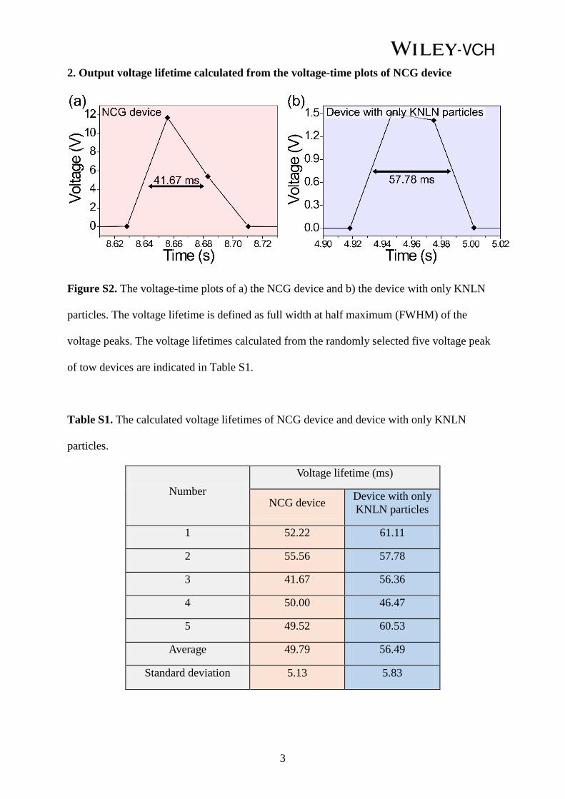
2. Output voltage lifetime calculated from the voltage-time plots of NCG device
Figure S2. The voltage-time plots of a) the NCG device and b) the device with only KNLN
particles. The voltage lifetime is defined as full width at half maximum (FWHM) of the
voltage peaks. The voltage lifetimes calculated from the randomly selected five voltage peak
of tow devices are indicated in Table S1.
Table S1. The calculated voltage lifetimes of NCG device and device with only KNLN
particles.
Number Voltage lifetime (ms)
NCG device Device with only KNLN particles
1 52.22 61.11
2 55.56 57.78
3 41.67 56.36
4 50.00 46.47
5 49.52 60.53
Average 49.79 56.49
Standard deviation 5.13 5.83
3
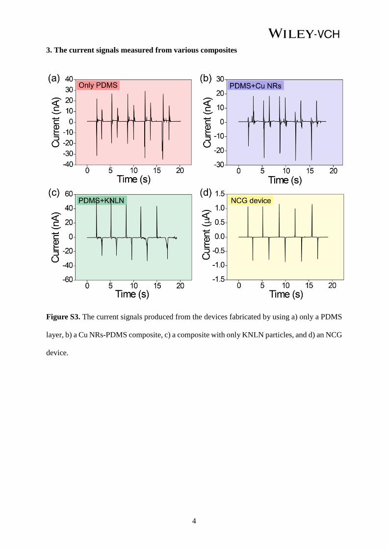
3. The current signals measured from various composites
Figure S3. The current signals produced from the devices fabricated by using a) only a PDMS
layer, b) a Cu NRs-PDMS composite, c) a composite with only KNLN particles, and d) an NCG
device.
4

4. The measurement results of KNLN-based NCG device with MW-CNTs instead of Cu
NRs
Figure S4. a) Output voltage (ii) and current (iii) measured from KNLN-based NCG device
with MW-CNTs when forward-connected (i) to a measurement unit. b) Ouput singals (ii and iii)
measured from an NCG device in reverse connection (i).
5

5. Dispersity of Cu NRs and MW-CNTs
Figure S5. a) SEM images of well-dispersed Cu NRs and one isolated Cu NR (inset). b) SEM
micrographs of easily-aggregated MW-CNTs and one MW-CNTs bundle (inset). Due to the
huge van der Waals force of MW-CNTs, one CNT strand is rarely isolated.
6
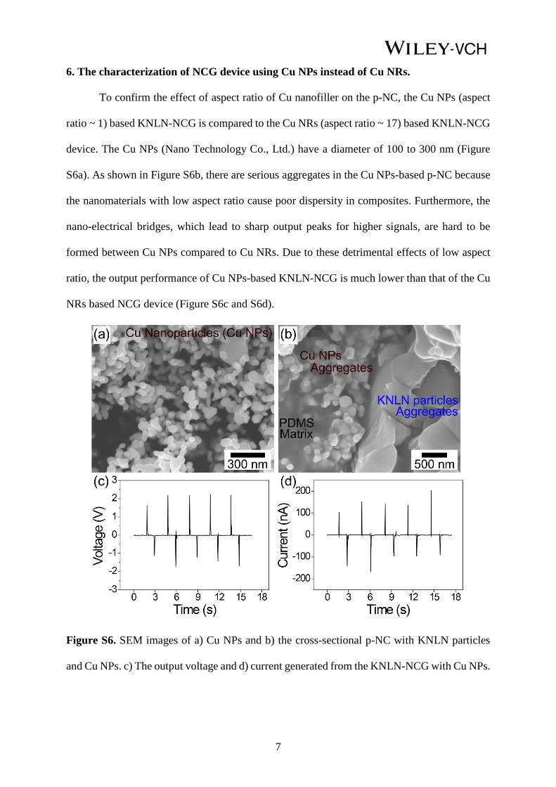
6. The characterization of NCG device using Cu NPs instead of Cu NRs.
To confirm the effect of aspect ratio of Cu nanofiller on the p-NC, the Cu NPs (aspect
ratio ~ 1) based KNLN-NCG is compared to the Cu NRs (aspect ratio ~ 17) based KNLN-NCG
device. The Cu NPs (Nano Technology Co., Ltd.) have a diameter of 100 to 300 nm (Figure
S6a). As shown in Figure S6b, there are serious aggregates in the Cu NPs-based p-NC because
the nanomaterials with low aspect ratio cause poor dispersity in composites. Furthermore, the
nano-electrical bridges, which lead to sharp output peaks for higher signals, are hard to be
formed between Cu NPs compared to Cu NRs. Due to these detrimental effects of low aspect
ratio, the output performance of Cu NPs-based KNLN-NCG is much lower than that of the Cu
NRs based NCG device (Figure S6c and S6d).
Figure S6. SEM images of a) Cu NPs and b) the cross-sectional p-NC with KNLN particles
and Cu NPs. c) The output voltage and d) current generated from the KNLN-NCG with Cu NPs.
7
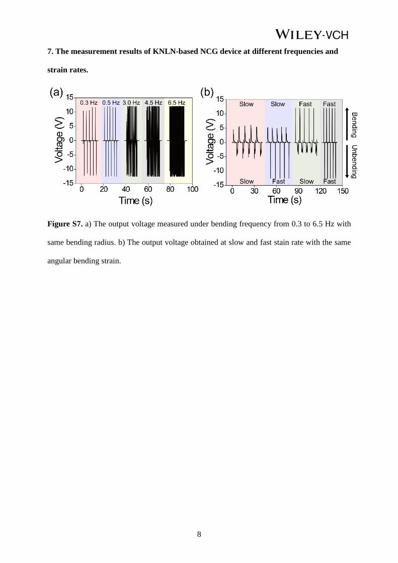
7. The measurement results of KNLN-based NCG device at different frequencies and
strain rates.
Figure S7. a) The output voltage measured under bending frequency from 0.3 to 6.5 Hz with
same bending radius. b) The output voltage obtained at slow and fast stain rate with the same
angular bending strain.
8
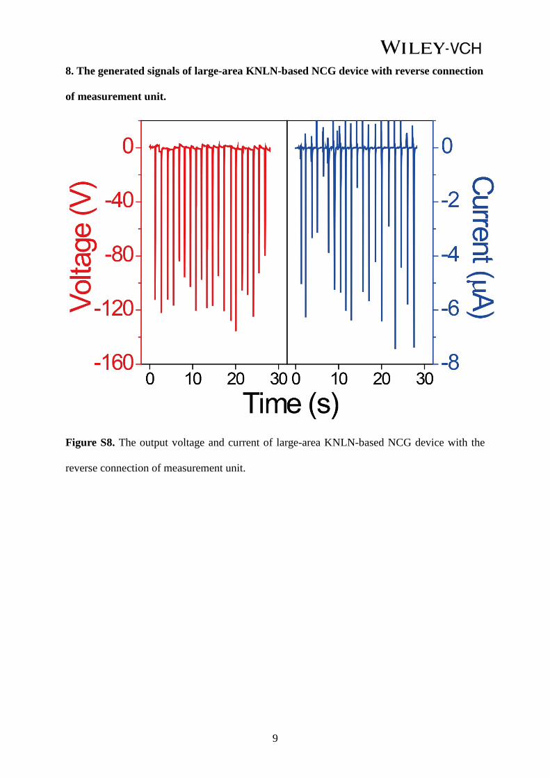
8. The generated signals of large-area KNLN-based NCG device with reverse connection
of measurement unit.
Figure S8. The output voltage and current of large-area KNLN-based NCG device with the
reverse connection of measurement unit.
9
9. The calculation for position of mechanically neutral region.
The distance between each cross-sectional center of three layers (top plastic, PDMS
matrix, and bottom plastic) and the mechanically neutral plane are y1 ~ y3, from up to down.
By the definition of mechanically neutral region, E1t1y1 + E2t2y2 + E3t3y3 = 0 has to be
satisfied, where E and t are Young’s modulus and thickness of each layer, respectively. The
effect of the PDMS matrix is negligible, since the modulus of PET plastic substrate (4 GPa) is
much larger than that of PDMS (1 ~ 2 MPa). By using the simultaneous equation with y1 – y3
= 362.5 μm, t1 = 50 μm, and t3 = 175 μm, y3 is solved as -80.5 μm, which means that the
mechanically neutral plane is 80.5 μm above the geometry center and 7 μm below the surface
of the bottom plastic substrate. Therefore, the mechanically neutral region is located inside the
bottom PET and below the p-NC/PDMS layers, resulting in entire tensile stress during bending
deformation.
10
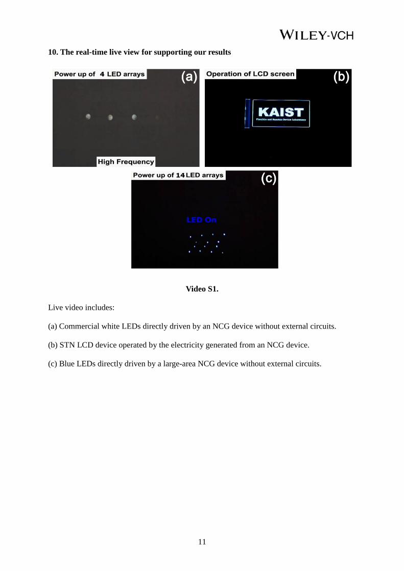
10. The real-time live view for supporting our results
Video S1.
Live video includes:
(a) Commercial white LEDs directly driven by an NCG device without external circuits.
(b) STN LCD device operated by the electricity generated from an NCG device.
(c) Blue LEDs directly driven by a large-area NCG device without external circuits.
11