---under construction--- sanyo icepower amp system …€¦ · tentative specification sheet no.:...
TRANSCRIPT
Tentative Specification Sheet No.:
1/26
---Under construction--- Sanyo ICEpower Amp System 1 LA4930/LV4970 - 2ch Analogue input, ICEpower power amplifier Version 0.4
Content Description......................................................................... 2 Applications........................................................................ 2 Features ............................................................................ 2 Absolute Maximum Ratings .................................................. 3 Normal Operating Conditions ................................................ 3 Electrical Characteristics Mode 1 (4Ω).................................... 3 Electrical Characteristics Mode 2 (8Ω).................................... 4 Pin descriptions................................................................... 4 Equivalent circuit block diagram............................................ 6 Typical Application (2x100W breadboad) .................................... 11 Interfacing with the chipset ................................................ 14 Protection ........................................................................ 16 Typical performance .......................................................... 24 Packages ......................................................................... 26 Sanyo Semiconductor Company 1-1-1, Sakata Oizumi-Machi Ora-Gun Gunma 370-0596, Japan Phone: [81] 276 61 8388, Fax: [81] 276 61 8730 www.semic.sanyo.co.jp/index_e.htm Bang & Olufsen ICEpower a/s Gl. Lundtoftevej 1b DK-2800 Lyngby, Denmark Phone [45] 45 20 36 00, Fax [45] 45 20 36 99 [email protected], www.icepower.bang-olufsen.com

2/26
Description
Sanyo ICEpower Amplifier System 1 is based on the ICEpower analog technology, consisting of unique COM modulation and MECC feedback control techniques, is adopted for the Amplifier System 1 to reach best in class audio performance. Sanyo ICEpower Amplifier System 1 consists of one LA4930 analogue 2ch controller IC and two LV4970 half bridge driver IC’s, which implements up to 150W pr. Channel output with a single ended (bridgeable) output stage operating from dual power supplies. New output stage drive technology, the Intelligent Power Cell (IPC), is adapted to reach state-of-the-art efficiency (95-96% in 8 ohm loading) and idle power consumption (<1W). The documentation describing the chipset consist of following documents:
• LA4930M datasheet. • LV4970M datasheet. • Sanyo ICEpower Amp System 1 LA4930/LV4970. • Application note.
Applications
• Car audio • Home audio • A/V receiver
Features
• High audio performance • THD+N = 0.005% @ 1W / 1 kHz, THD+N < 0.05% all frequencies and output powers. • Idle Noise = 50 µV Awtd, typical • Bandwidth typical: 80kHz (programmable)
• High undistorted output power
• Po=100W/ch, THD+N=0.05%, 4 ohm, 1kHz, (Vd,Vs=±40V) • Po2=100W/ch, THD+N=0.05%, 8 ohm, 1kHz, (Vd,Vs=±50V) • Max output = 150W, THD+N = 0.05%, 8 ohm • Max output = 200W, THD+N = 0.05%, 4 ohm (SE or BTL mode )
• Total protection scheme
• Local over current limit at each FET & Output short circuit protection • Over voltage protection • Optional under voltage protection • Thermal protection • High frequency / output filter protection.
• Sound quality optimized intelligent input soft clipping. • Flexibility in MECC control system design provided by external components.
3/26
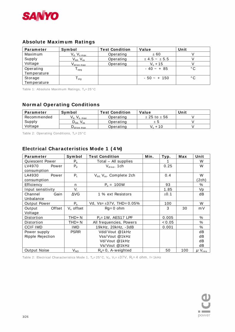
Absolute Maximum Ratings
Parameter Symbol Test Condition Value Unit Vd, Vs max Operating ± 60 V Vdd, Vss Operating ± 4.5 ~ ± 5.5 V
Maximum Supply Voltage Vdrive max Operating Vs +15 V Operating Temperature
Topg - 40 ~ + 85 °C
Storage Temperature
Tstg - 50 ~ + 150 °C
Table 1: Absolute Maximum Ratings, Ta=25°C
Normal Operating Conditions
Parameter Symbol Test Condition Value Unit Vd, Vs, max Operating ± 25 to ± 56 V Ddd, Vss Operating ± 5 V
Recommended Supply Voltage Ddrive max Operating Vs +10 V
Table 2: Operating Conditions, Ta=25°C
Electrical Characteristics Mode 1 (4Ω)
Parameter Symbol Test Condition Min. Typ. Max Unit Quiescent Power Pq Total – All supplies 1 W LV4970 Power consumption
Pd Vdrive. 1ch 0.25 W
LA4930 Power consumption
Pc Vdd, Vss. Complete 2ch 0.4 W (2ch)
Efficiency n Po = 100W 93 % Input sensitivity Vi 1.85 Vp Channel Gain Unbalance
∆VG 1 % ext Resistors ±0.1 dB
Output Power Po Vd, Vs=±37V, THD=0.05% 100 W Output Offset Voltage
Vn offset Rg=0 ohm 3 30 mV
Distortion THD+N Po=1W, AES17 LPF 0.005 % Distortion THD+N All frequencies, Powers <0.05 % CCIF IMD IMD 19kHz, 20kHz, -3dB 0.001 % Power supply Ripple Rejection
PSRR Vdd/Vout @1kHz Vss/Vout @1kHz Vd/Vout @1kHz Vs/Vout @1kHz
dB dB dB dB
Output Noise VNO Rg=0, A-weighted 50 100 μ Vrms
Table 2: Electrical Characteristics Mode 1, Ta=25°C, Vd, Vs=±37V, RL=4 ohm, f=1kHz
4/26
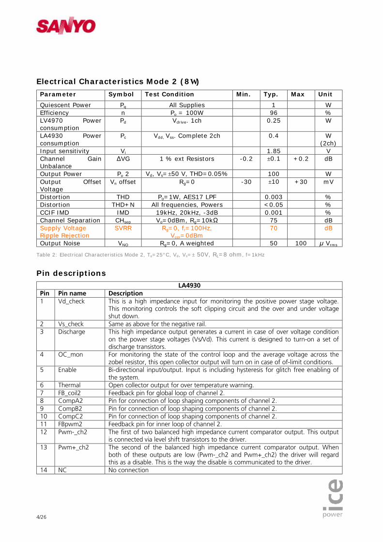
Electrical Characteristics Mode 2 (8Ω)
Parameter Symbol Test Condition Min. Typ. Max Unit
Quiescent Power Pq All Supplies 1 W Efficiency n Po = 100W 96 % LV4970 Power consumption
Pd Vdrive. 1ch 0.25 W
LA4930 Power consumption
Pc Vdd, Vss. Complete 2ch 0.4 W (2ch)
Input sensitivity Vi 1.85 V Channel Gain Unbalance
∆VG 1 % ext Resistors -0.2 ±0.1 +0.2 dB
Output Power Po 2 Vd, Vs=±50 V, THD=0.05% 100 W Output Offset Voltage
Vn offset Rg=0 -30 ±10 +30 mV
Distortion THD Po=1W, AES17 LPF 0.003 % Distortion THD+N All frequencies, Powers <0.05 % CCIF IMD IMD 19kHz, 20kHz, -3dB 0.001 % Channel Separation CHsep Vo=0dBm, Rg=10kΩ 75 dB Supply Voltage Ripple Rejection
SVRR Rg=0, fr=100Hz, Vccr=0dBm
70 dB
Output Noise VNO Rg=0, A weighted 50 100 μ Vrms
Table 2: Electrical Characteristics Mode 2, Ta=25°C, Vd, Vs=± 50V, RL=8 ohm, f=1kHz
Pin descriptions
LA4930 Pin Pin name Description 1 Vd_check This is a high impedance input for monitoring the positive power stage voltage.
This monitoring controls the soft clipping circuit and the over and under voltage shut down.
2 Vs_check Same as above for the negative rail. 3 Discharge This high impedance output generates a current in case of over voltage condition
on the power stage voltages (Vs/Vd). This current is designed to turn-on a set of discharge transistors.
4 OC_mon For monitoring the state of the control loop and the average voltage across the zobel resistor, this open collector output will turn on in case of of-limit conditions.
5 Enable Bi-directional input/output. Input is including hysteresis for glitch free enabling of the system.
6 Thermal Open collector output for over temperature warning. 7 FB_coil2 Feedback pin for global loop of channel 2. 8 CompA2 Pin for connection of loop shaping components of channel 2. 9 CompB2 Pin for connection of loop shaping components of channel 2. 10 CompC2 Pin for connection of loop shaping components of channel 2. 11 FBpwm2 Feedback pin for inner loop of channel 2. 12 Pwm-_ch2 The first of two balanced high impedance current comparator output. This output
is connected via level shift transistors to the driver. 13 Pwm+_ch2 The second of the balanced high impedance current comparator output. When
both of these outputs are low (Pwm-_ch2 and Pwm+_ch2) the driver will regard this as a disable. This is the way the disable is communicated to the driver.
14 NC No connection
5/26
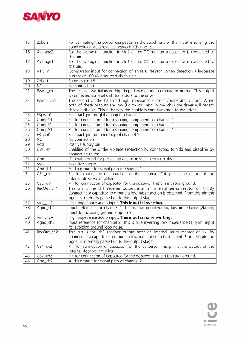
15 Zobel2 For estimating the power dissipation in the zobel resistor this input is sensing the zobel voltage via a resistive network. Channel 2.
16 Average2 For the averaging function in ch 2 of the OC monitor a capacitor is connected to this pin.
17 Average1 For the averaging function in ch 1 of the OC monitor a capacitor is connected to this pin.
18 NTC_in Comparator input for connection of an NTC resistor. When detection a hysterese current of 100uA is sourced via this pin.
19 Zobel1 Same as pin 15 20 NC No connection 21 Pwm-_ch1 The first of two balanced high impedance current comparator output. This output
is connected via level shift transistors to the driver. 22 Pwm+_ch1 The second of the balanced high impedance current comparator output. When
both of these outputs are low (Pwm-_ch1 and Pwm+_ch1) the driver will regard this as a disable. This is the way the disable is communicated to the driver.
23 FBpwm1 Feedback pin for global loop of channel 1 24 CompC1 Pin for connection of loop shaping components of channel 1 25 CompB1 Pin for connection of loop shaping components of channel 1 26 CompA1 Pin for connection of loop shaping components of channel 1 27 FB_coil1 Feedback pin for inner loop of channel 1 28 NC No connection 29 Vdd Positive supply pin 30 UVP_en Enabling of the Under Voltage Protection by connecting to Vdd and disabling by
connecting to Vss. 31 Gnd General ground for protection and all miscellaneous circuits. 32 Vss Negative supply 33 Gnd ch1 Audio ground for signal path of channel 1 34 CS1_ch1 Pin for connection of capacitor for the dc servo. This pin is the output of the
internal dc servo amplifier. 35 CS2_ch1 Pin for connection of capacitor for the dc servo. This pin is virtual ground. 36 RecOut_ch1 This pin is the ch1 receiver output after an internal series resistor of 1k. By
connecting a capacitor to ground a low pass function is obtained. From this pin the signal is internally passed on to the output stage.
37 Vin__ch1- High impedance audio input. This input is inverting. 38 Agnd_ch1 Input reference for channel 1. This is true non-inverting low impedance (2kohm)
input for avoiding ground loop noise. 39 Vin_ch2+ High impedance audio input. This input is non-inverting. 40 Agnd_ch2 Input reference for channel 2. This is true inverting low impedance (1kohm) input
for avoiding ground loop noise. 41 RecOut_ch2 This pin is the ch2 receiver output after an internal series resistor of 1k. By
connecting a capacitor to ground a low pass function is obtained. From this pin the signal is internally passed on to the output stage.
42 CS1_ch2 Pin for connection of capacitor for the dc servo. This pin is the output of the internal dc servo amplifier.
43 CS2_ch2 Pin for connection of capacitor for the dc servo. This pin is virtual ground. 44 Gnd_ch2 Audio ground for signal path of channel 2
6/26
LV4970
Pin Pin name description 1 Sense1_H This High-Z pin sources 200uA for the use of the over current sensing. 2 Sense2_H This High-Z pin sinks 100uA. This ensures that the current is equal in the to sense
diodes. 3 NC No Connection 4 NC No Connection 5 Pwm+ Low-Z non-inverting current input 6 Pwm- Low-Z inverting current input 7 SS_en Safe start enabling input. 8 Blanking Blanking delay is controlled with this pin by connecting a resistor to ground.
Shorting the pin to ground the shortest blanking delay is achieved, while leaving the pin open will provide the maximum.
9 Vs Negative supply voltage 10 L_drive Driver output for low side power mosfet. 11 V_drive Positive supply voltage 12 Sense2_L This High-Z pin sources 200uA for the use of the over current sensing. 13 Sense1_L This High-Z pin sinks 100uA. This ensures that the current is equal in the to sense
diodes. 14 High_Re Reference pin for the floating high side driver. This pin is connected to the half
bridge output. 15 H_Drive High side driver output. 16 Vboot Bootstrap voltage. Floating supply voltage pin for highside driver.
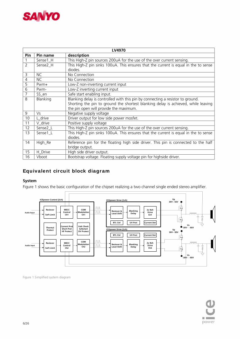
Equivalent circuit block diagram
System Figure 1 shows the basic configuration of the chipset realizing a two channel single ended stereo amplifier.
Reciever
Soft Limit
Reciever &Level ShiftAudio Input
ThermalProtect
Current ProtShort ProtHF Protect
Volt CheckSafestart
OV Protect
MECCControl
Ch1
COMModulation
Ch1
Reciever
Soft Limit
MECCControl
Ch2
COMModulation
Ch2Reciever &Level Shift
BlankingDelay
BlankingDelay
2x NchDriveCh1
2x NchDriveCh2
Current DetUV ProtBTL Ctrl
Current DetUV ProtBTL Ctrl
ICEpower Control (2ch) ICEpower Drive (1ch)
ICEpower Drive (1ch)
Audio Input
Vp30V - 55V
Vp30V - 55V
Vs-30V - -55V
Vs-30V - -55V
Figure 1 Simplified system diagram
7/26
LA4930 (Control)
RECout_ch2
FB
pw
m1
Average1
VD/VS
And Vdd/Vss
Check
(Global Protect.)
Enable
Average2
Comparator
Control
Receiver, clip control
and DC servo
Local disable
Local
protection Ch2
Comparator
Control
Receiver, clip control
and DC servo
Local
protection Ch1
Co
mpC
2
Pwm+_ch2
Zobel2
Voltage And current Reference
Thermal
NTC_in
1
Zobel1
Pwm-_ch2
Pwm+_ch1
Pwm-_ch1
Discharge
Vd_check
Com
pA
2
Vs_check
Co
mp
B2
FB
coil2
OC_mon
FB
coil
1
Com
pA
1
Com
pC
1
Com
pB
1
Vdd
Gnd
UVP_en
CS1_ch1
Gnd_ch2
Gnd_ch1
Vss
Agnd_ch1
CS2_ch2
Vin_ch1-
RECout_ch1
CS2_ch1
Agnd_ch2
CS1_ch2
Vin_ch2+
Thermal
Protection
LA4930
9
3
4
10
7
5
18
11
12
8
13
15
16
2
6
19
21
17
22
23
24
25
2627
42
29
30
31
32
33
34
35
36
41
37
38
39
40
43
44
14
20
26
NC
NC
NC
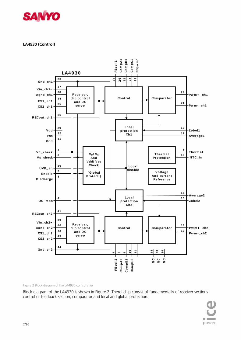
Figure 2 Block diagram of the LA4930 control chip
Block diagram of the LA4930 is shown in Figure 2. Therol chip consist of fundamentally of receiver sections control or feedback section, comparator and local and global protection.

8/26
Receiver The receiver is a versatile input engine with a broad range of features.
• The receiver has a high impedance input terminal for applying single ended signal, it also have a low impedance reversed input terminal for rejecting ground noise. For obtaining good channel separation the ground connections for the analog circuits of each channel has been pinned out separately.
• The receiver has a soft clipping circuit that performs a controlled clipping according to the voltage applied to the output stage. The clipping level will always be Vd*0.875 for the positive waves and equally Vs*0.875 for the negative waves. This feature secures that the control system is never saturated during normal operation and eliminates clipping with recovery time, which produce a very harsh clipping sound. The clipping circuit has a soft clipping characteristics producing is very pleasant clipping sound.
• For the recommended schematics the input clip level is always 1.86Vp no matter what voltage applied to the output stage. The design procedure of the control system will result in a gain, which always provides the standard clip level.
• A dc servo is built in the receiver to secure low pop noise during start-up. • Lowpass filtering. • Channel inversion for better use of buffer capacitors in power supply.
Control In this block all feedback circuitry is gathered.
• Feedback before and after filter. This means less coil requirements and better frequency response. • Flexible loop control for various properties set by external components. • Easy to use table recommendations available in application note.
Comparator This is where the analog signals enter the PWM domain and following features are included.
• Fast low power comparator. • Differential output for fast and noiseless level shift without excessive power dissipation in the level shift. • Enable signal coded into the 2 outputs.
Protection It is here beneficial to distinguish between the local protection features and the global protection features. Local protection refers to a protection feature, which are measuring and acting on the same channel only. Where as the global protection measures on shared items and act globally via the enable bus. The local protection (zobel protection and OC detection) consists of:
• Zobel protection to protect against excessive power dissipation in the zobel resistor. • Saturation detection referred to as OC protection. • DC protection on output.
When a local protection feature is acting the OC monitor bus is pulled down. Both channels share the same bus and are connected internally by open collectors. The channel is shut down by disabling the comparator output. The Global protection features:
• Under/over voltage of the power stage (Vd/Vs) • Under voltage of the control supply voltage (Vdd/Vss)
The global protection act directly on the enable bus and the enable bus state is forwarded by the global protection to the local protection blocks. The local protection are now shut down the amplifier. In the case of multi channel systems, sharing the same enable bus all chipset are shutdown.
9/26
Thermal protection Finally a thermal warning function is included. This function basically works independently and is connected via an open collector to the thermal bus. This function is a simple over temperature indication including hysteresis, which can be adjusted by external components.
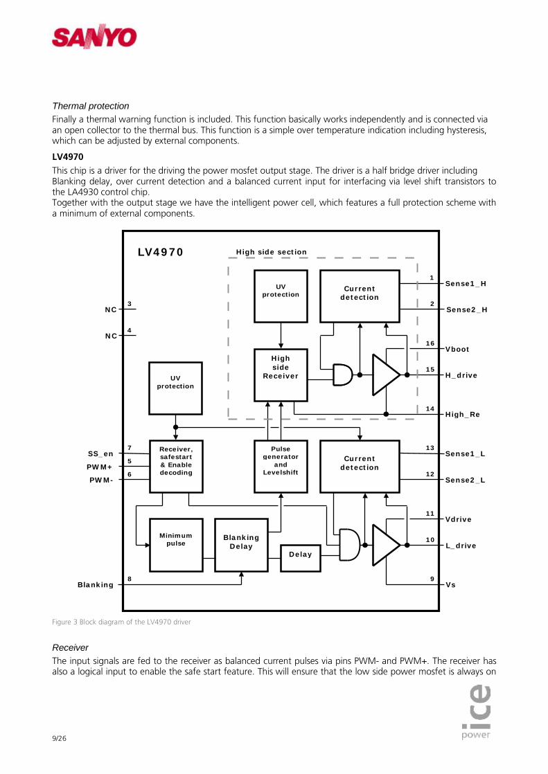
LV4970 This chip is a driver for the driving the power mosfet output stage. The driver is a half bridge driver including Blanking delay, over current detection and a balanced current input for interfacing via level shift transistors to the LA4930 control chip. Together with the output stage we have the intelligent power cell, which features a full protection scheme with a minimum of external components.
PWM+
Receiver, safestart & Enable decoding
Vs
Delay
Minimum
pulse
Blanking
Delay
Current
detection
High side
Receiver
L_drive
Vdrive
High_Re
H_drive
SS_en
NC
Blanking
NC
LV4970
5
15
10
11
9
16
3
4
6
8
PWM-
Current
detection
UV protection
Pulse generator
and Levelshift
Vboot
7
Sense1_H
Sense2_H
Sense2_L
Sense1_L
1
2
14
13
12
High side section
UV
protection
Figure 3 Block diagram of the LV4970 driver
Receiver The input signals are fed to the receiver as balanced current pulses via pins PWM- and PWM+. The receiver has also a logical input to enable the safe start feature. This will ensure that the low side power mosfet is always on
10/26
for 2us after power-up or after enabling. With this feature enabled, the bootstrap capacitor will always be charged in an controlled way during start-up. The receiver outputs the PWM as a normal voltage mode logic PWM signal together with the decoded enable signal. Minimum pulse The PWM signal now reaches he minimum pulse circuit, which ensures that the minimum pulse length will not exceed 200ns typically. If a pulse occurs with less duration than 200ns, the pulse will be prolonged to 200ns. Blanking delay Next is the blanking delay which provide the blanking delay to prevent shot through currents in the output stage, here the PWM signal is split into a high side signal and a lowside signal. The lowside PWM signal is now delayed in order to match the delay in the high side in lowside. Finally the lowside PWM signal is AND’et with to protection signals and then connected to the output drive. Pulse generator and level shift From the blanking delay block the high side PWM signal is converted into a set and reset pulse and level shifted to the high side section of the die. High side receiver The high side receiver features a patented low impedance input circuitry with common mode rejection for fast, reliable and efficient level shift. The high side driver also contains a under voltage protection. The high side PWM signal is now AND’et with the Over Current detection and connected to the High side driver. The OC protection The over current detection circuit is basically the same in the high side and low side and it works by measuring the voltage across the mosfets during the on time. The timing for detecting the on time is done by evaluating the signals before and after the driver stage. In case of detection the driver is shutdown for 1.25us causing the amplifier to enter a current mode oscillation, where the output stage will act as a current generator while the control system is trying to force a output current larger than the limit. In effect the output current will be limited in the same way as most conventional class-AB output stages but here we are still operating in class-D with high efficiency. Even though the current limitation mode is class-d the power dissipation in the output stage is relatively high (typ. 4-8W) and therefore a time limit is build in before shut down. The current limitation mode is determined in the control chip by detecting saturation of the control system. This condition will typically be allowed in 100ms to 500ms enough for avoiding shutdown during peak currents during high music output power.
Output drive The output stage is designed to drive the mosfets with a Qg less than 40nC directly. The 40nC case will lead to a power dissipation of approximately 350mW in the driver package.
11/26
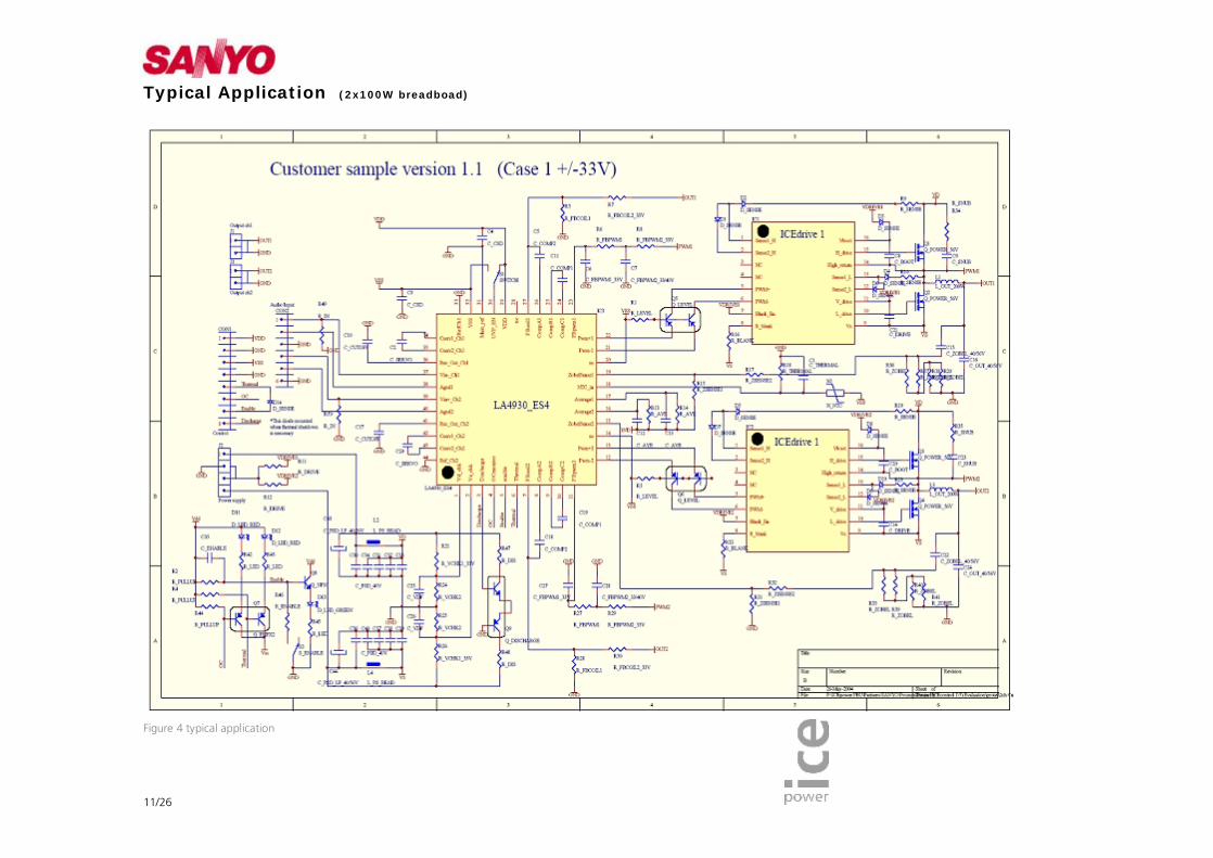
Typical Application (2x100W breadboad)
Figure 4 typical application


13/26
The typical application schematic is described in details in application note: Anxxx This application notes contains detailed description of the customer breadboards which in standard versions are available in three different voltages: +/-33, +/-40 and +/-56Volt.
14/26
Interfacing with the chipset
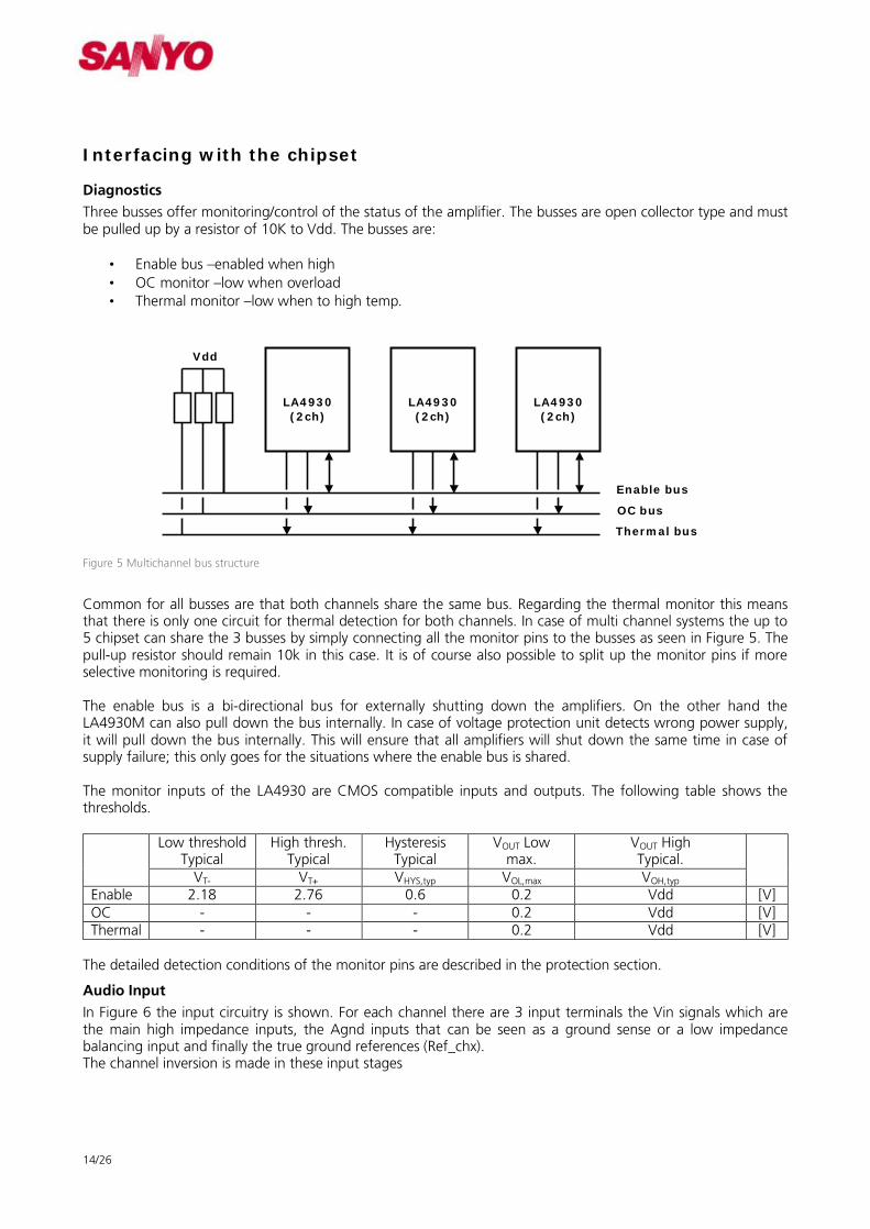
Diagnostics Three busses offer monitoring/control of the status of the amplifier. The busses are open collector type and must be pulled up by a resistor of 10K to Vdd. The busses are:
• Enable bus –enabled when high • OC monitor –low when overload • Thermal monitor –low when to high temp.
LA4930 (2ch)
LA4930 (2ch)
LA4930 (2ch)
Enable bus
OC bus
Thermal bus
Vdd
Figure 5 Multichannel bus structure
Common for all busses are that both channels share the same bus. Regarding the thermal monitor this means that there is only one circuit for thermal detection for both channels. In case of multi channel systems the up to 5 chipset can share the 3 busses by simply connecting all the monitor pins to the busses as seen in Figure 5. The pull-up resistor should remain 10k in this case. It is of course also possible to split up the monitor pins if more selective monitoring is required. The enable bus is a bi-directional bus for externally shutting down the amplifiers. On the other hand the LA4930M can also pull down the bus internally. In case of voltage protection unit detects wrong power supply, it will pull down the bus internally. This will ensure that all amplifiers will shut down the same time in case of supply failure; this only goes for the situations where the enable bus is shared. The monitor inputs of the LA4930 are CMOS compatible inputs and outputs. The following table shows the thresholds.
Low threshold Typical
High thresh. Typical
Hysteresis Typical
VOUT Low max.
VOUT High Typical.
VT- VT+ VHYS,typ VOL,max VOH,typ
Enable 2.18 2.76 0.6 0.2 Vdd [V] OC - - - 0.2 Vdd [V] Thermal - - - 0.2 Vdd [V]
The detailed detection conditions of the monitor pins are described in the protection section.
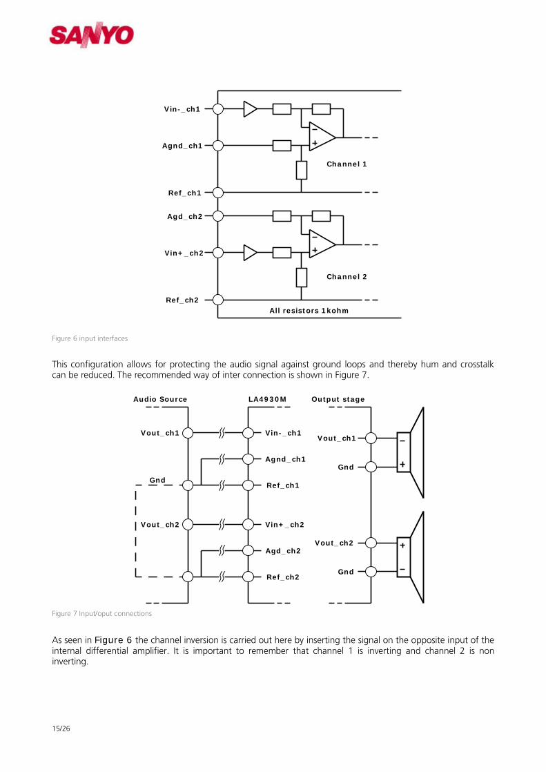
Audio Input In Figure 6 the input circuitry is shown. For each channel there are 3 input terminals the Vin signals which are the main high impedance inputs, the Agnd inputs that can be seen as a ground sense or a low impedance balancing input and finally the true ground references (Ref_chx). The channel inversion is made in these input stages
15/26
Agd_ch2
Ref_ch1
Agnd_ch1
Vin-_ch1
Channel 1
Channel 2
Vin+_ch2
Ref_ch2 All resistors 1kohm
Figure 6 input interfaces
This configuration allows for protecting the audio signal against ground loops and thereby hum and crosstalk can be reduced. The recommended way of inter connection is shown in Figure 7.
Agd_ch2
Ref_ch1
Agnd_ch1
Vout_ch1
Vin+_ch2
Ref_ch2
LA4930M Audio Source
Vout_ch2
Gnd
Vin-_ch1
Output stage
Gnd
Gnd
Vout_ch1
Vout_ch2
Figure 7 Input/oput connections
As seen in Figure 6 the channel inversion is carried out here by inserting the signal on the opposite input of the internal differential amplifier. It is important to remember that channel 1 is inverting and channel 2 is non inverting.
16/26
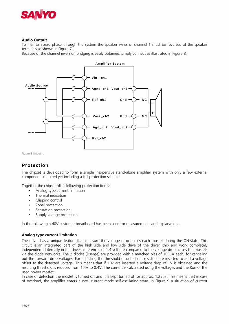
Audio Output To maintain zero phase through the system the speaker wires of channel 1 must be reversed at the speaker terminals as shown in Figure 7. Because of the channel inversion bridging is easily obtained, simply connect as illustrated in Figure 8.
Agd_ch2
Ref_ch1
Agnd_ch1
Vin+_ch2
Ref_ch2
Amplifier System
Audio Source
Vin-_ch1
NC
NC Gnd
Gnd
Vout_ch1
Vout_ch2
Figure 8 Bridging
Protection The chipset is developed to form a simple inexpensive stand-alone amplifier system with only a few external components required yet including a full protection scheme. Together the chipset offer following protection items:
• Analog type current limitation • Thermal indication • Clipping control • Zobel protection • Saturation protection • Supply voltage protection
In the following a 40V customer breadboard has been used for measurements and explanations.
Analog type current limitation The driver has a unique feature that measure the voltage drop across each mosfet during the ON-state. This circuit is an integrated part of the high side and low side drive of the driver chip and work completely independent. Internally in the driver, references of 1.4 volt are compared to the voltage drop across the mosfets via the diode networks. The 2 diodes (Dsense) are provided with a matched bias of 100uA each, for canceling out the forward drop voltages. For adjusting the threshold of detection, resistors are inserted to add a voltage offset to the detected voltage. This means that if 10k are inserted a voltage drop of 1V is obtained and the resulting threshold is reduced from 1.4V to 0.4V. The current is calculated using the voltages and the Ron of the used power mosfet. In case of detection the mosfet is turned off and it is kept turned of for approx. 1.25uS. This means that in case of overload, the amplifier enters a new current mode self-oscillating state. In Figure 9 a situation of current

17/26
limitation is shown. The amplifier is loaded with 1 ohm and a single cycle of 5kHz is applied and when the voltage reaches 15V corresponding to 15A, the amplifier enters the current limitation state. The switching frequency of the current limitation state is about 300kHz at this output voltage.
Figure 9 5Khz into 1 ohm load
This unique feature provides a continuous transition between normal voltage mode and current mode like the behavior of an analog system. When the amplifier enters the current mode the voltage mode control loop is overruled and the control chip will saturate but not shutdown. Figure 10 illustrates this by applying first a 10Vp cycle where there is no current limitation and then a cycle including current limitation. The other trace is the virtual ground pin of the modulator amp.
Figure 10 Shot of saturation of control sys.
18/26
It can be seen on virtual ground trace that it clearly saturates when the amplifier enters current limitation. This is an important point because detecting saturation in this way is actually used internally in the chip as a mean of detecting over current and other overload situations. It is very important to realize that there is no direct communication between the driver and control chip in the case of the amplifier entering current limitation. When the control chip is detecting the current limitation situation, it is solely detected from saturation of the loop. There is build in a time limit of the over current situation, which is described in the saturation protection section.
Thermal indication With this class-D amplifier system efficiencies of up to 96% can be reached this means that very powerful amplifiers of 2X150W amplifiers can be realized using only PCB cooling. I normal condition the thermal detection will not act if the mechanical system is well designed, even with an output of 2x150W clipped music. Since the thermal indication is not expected during normal situations the thermal detection is a simple over temperature detection. Even though the efficiency is very high there are situations where the temperature can exceed maximum. The worst situation is a wrong loading of 1-3 ohm with full voltage swing. In this case the current limitation will only act for short periods and the time limit for current limitation may not be reached. This means that the output stage will dissipate a considerable amount of power and will eventually overheat and the thermal detection will act. In the case of short circuit (0.6 ohm) the current detection will limit the current in most of the time when applied a music signal. The time out of the current limitation will be reached fast and the amplifier will be shut down. The thermal characteristics of course depend of the mechanical system and it is recommended to read the application note of the costumer breadboard where information on thermal design of PCB is written.
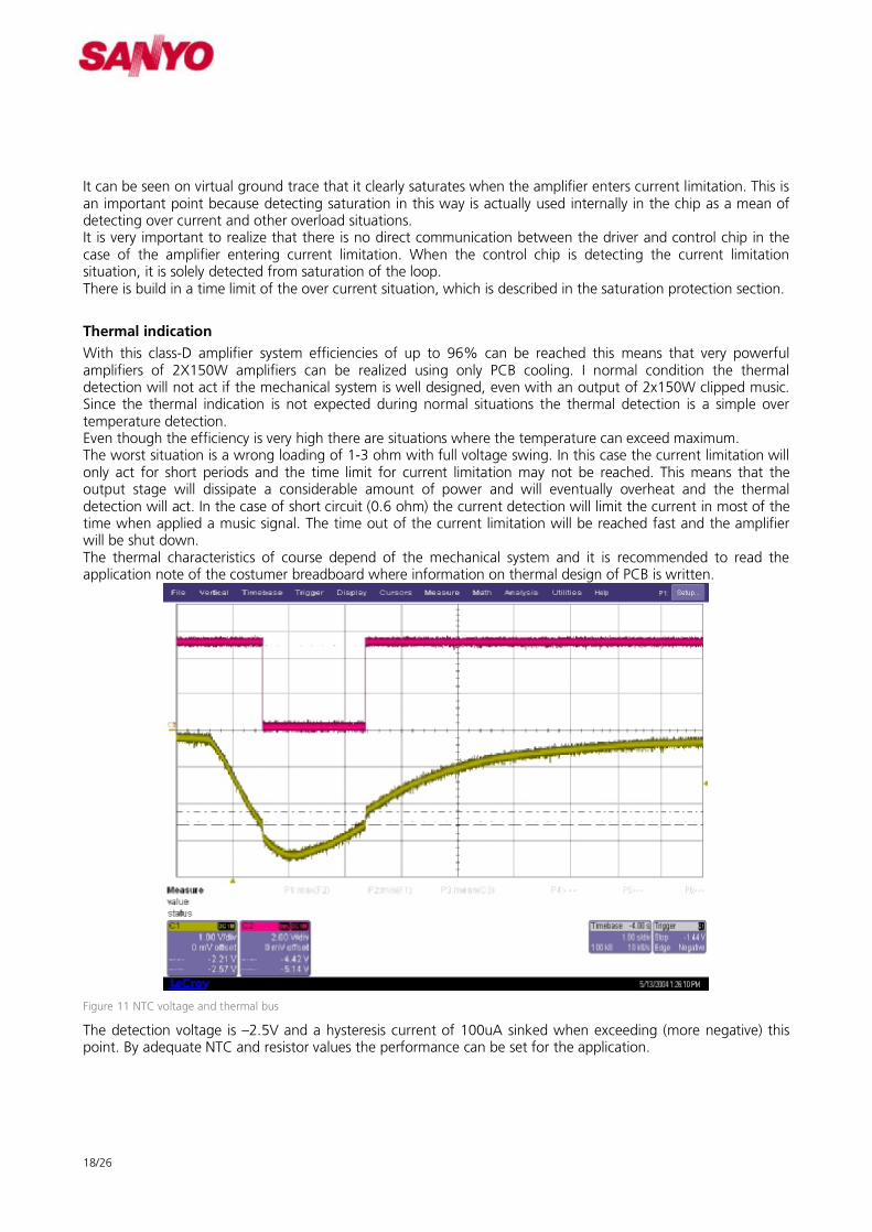
Figure 11 NTC voltage and thermal bus
The detection voltage is –2.5V and a hysteresis current of 100uA sinked when exceeding (more negative) this point. By adequate NTC and resistor values the performance can be set for the application.
19/26
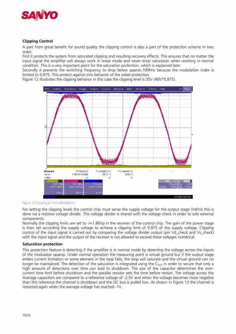
Clipping Control A part from great benefit for sound quality the clipping control is also a part of the protection scheme in two ways: First it protects the system from saturated clipping and resulting recovery effects. This ensures that no matter the input signal the amplifier will always work in linear mode and never enter saturation when working in normal condition. This is a very important point for the saturation protection, which is explained later. Secondly it prevents the switching frequency to drop below approx.100kHz because the modulation index is limited to 0.875. This protect against miss behavior of the zobel protection. Figure 12 illustrates the clipping behavior in this case the clipping level is 35V (40V*0,875).
Figure 12 Clipping at 1khz 80W/8ohm
For setting the clipping levels the control chip must sense the supply voltage for the output stage (Vd/Vs) this is done via a resistive voltage divider. This voltage divider is shared with the voltage check in order to safe external components. Normally the clipping limits are set to -/+1.86Vp in the receiver of the control chip. The gain of the power stage is then set according the supply voltage to achieve a clipping limit of 0.875 of the supply voltage. Clipping control of the input signal is carried out by comparing the voltage divider output (pin Vd_check and Vs_check) with the input signal and the output of the receiver is not allowed to exceed these voltages numerical.
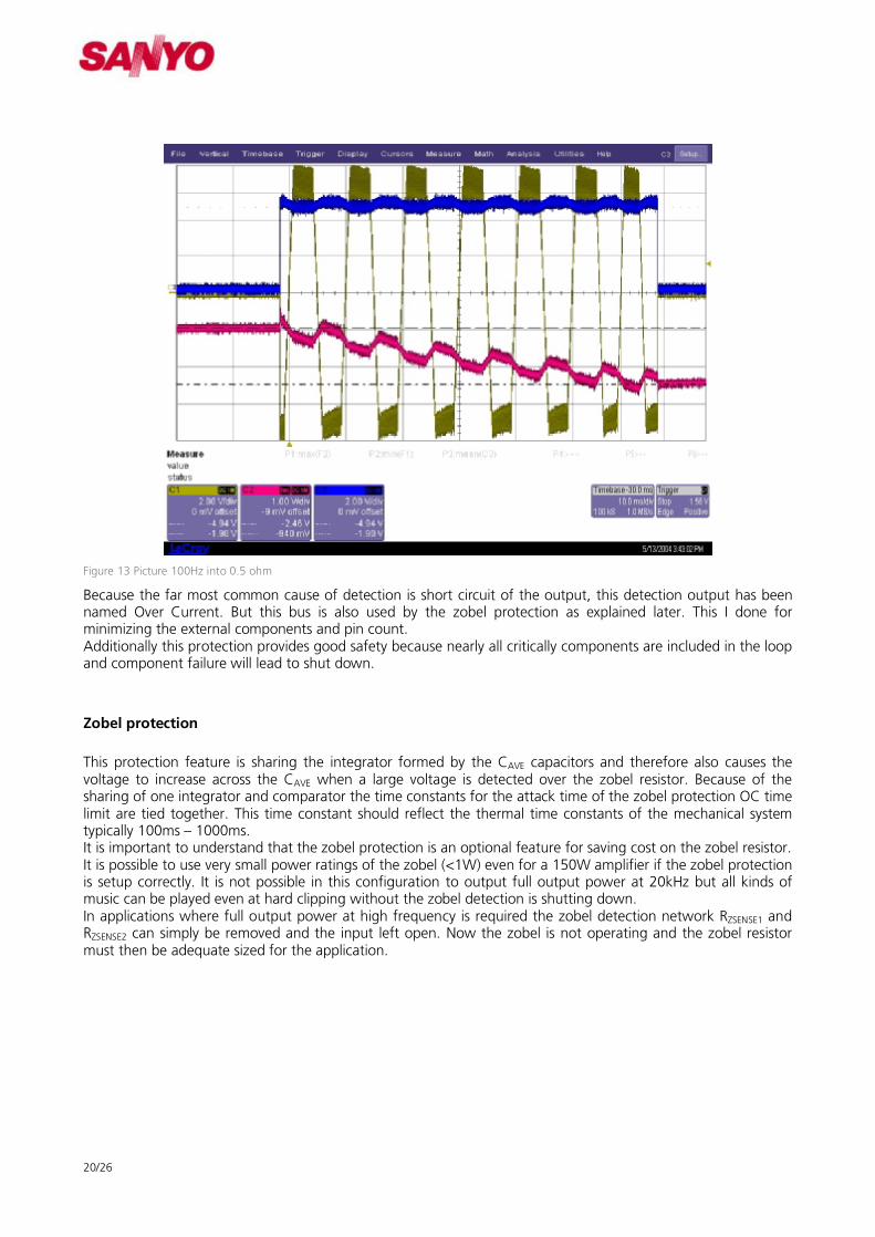
Saturation protection This protection feature is detecting if the amplifier is in normal mode by detecting the voltage across the inputs of the modulator opamp. Under normal operation the measuring point is virtual ground but if the output stage enters current limitation or some element in the loop fails, the loop will saturate and the virtual ground can no longer be maintained. The detection of the saturation is integrated using the CAVE in order to secure that only a high amount of detections over time can lead to shutdown. The size of the capacitor determines the over-current time limit before shutdown and the parallel resistor sets the time before restart. The voltage across the Average capacitors are compared to a reference voltage of -2.5V and when the voltage becomes more negative than this reference the channel is shutdown and the OC bus is pulled low. As shown in Figure 13 the channel is restarted again when the average voltage has reached -1V.
20/26
Figure 13 Picture 100Hz into 0.5 ohm
Because the far most common cause of detection is short circuit of the output, this detection output has been named Over Current. But this bus is also used by the zobel protection as explained later. This I done for minimizing the external components and pin count. Additionally this protection provides good safety because nearly all critically components are included in the loop and component failure will lead to shut down.
Zobel protection This protection feature is sharing the integrator formed by the CAVE capacitors and therefore also causes the voltage to increase across the CAVE when a large voltage is detected over the zobel resistor. Because of the sharing of one integrator and comparator the time constants for the attack time of the zobel protection OC time limit are tied together. This time constant should reflect the thermal time constants of the mechanical system typically 100ms – 1000ms. It is important to understand that the zobel protection is an optional feature for saving cost on the zobel resistor. It is possible to use very small power ratings of the zobel (<1W) even for a 150W amplifier if the zobel protection is setup correctly. It is not possible in this configuration to output full output power at 20kHz but all kinds of music can be played even at hard clipping without the zobel detection is shutting down. In applications where full output power at high frequency is required the zobel detection network RZSENSE1 and RZSENSE2 can simply be removed and the input left open. Now the zobel is not operating and the zobel resistor must then be adequate sized for the application.
21/26
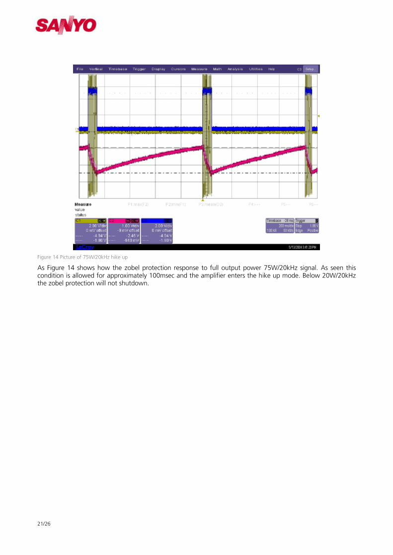
Figure 14 Picture of 75W/20kHz hike up
As Figure 14 shows how the zobel protection response to full output power 75W/20kHz signal. As seen this condition is allowed for approximately 100msec and the amplifier enters the hike up mode. Below 20W/20kHz the zobel protection will not shutdown.

22/26
Supply voltage protection In the control chip there is build in under/over voltage detection of the power stage supplies (Vd/Vs) and also a under voltage lockout of the Control supply voltages (Vdd/Vss). The over voltage protection is mainly to protect against supply pumping. A short explanation of supply pumping in a single ended class-d power stage: Considering a class-b output stage powered by +/-20V and the output voltage is 10 VDC into a 10 ohm load. The output current is now 1A and the power dissipation in the amplifier and load is then 10W each. In the class-b situation the current in the negative supply is zero and the power dissipation is caused by having voltage and current present at the same time. Now if we have a class-d power stage including output filter the output current would be still be 1 A but the high side current would be 0.75 ARMS because the voltage swing requires a modulation index of 0.75. Since the class-d theoretically has an efficiency of 100%, the output stage must pump energy back in the negative supply to preserve the energy. The current pumped back is 0.25ARMS and for a negative output current the pumping will occur at the positive supply. Since most power supplies are not uni-directional the pumping result in voltage peaks on the supplies especially at low frequencies. This is shown in Figure 15. Where the supply rails is jumping from +/-40V up to approx. +/-48V. The maximum pumping occurs when the output voltage is half of the rail voltage so therefore the maximum pumping is not seen at full output swing but when the average of the waveform is half the rail voltage.
Figure 15 Supply pump at 20Hz/30W/8 ohm
The normal way of dealing with this problem is to add sufficient capacitance in the power supply. As rule of thumb it takes 2x1000uF to output 100W in 8 ohm when the amplifier is supplied with +/- 50V. The supply pumping will be less than 25% in this case for a 20Hz sine. The over voltage threshold in the standard recommendations is set to be 135% of the nominal supply voltage. In the case of detection the amplifier is shut down and a discharge feature activates. This feature enables a discharge sequence of the supply capacitors. This prevents a very long shutdown time because in the case amplifier shutdown the current draw on Vd/Vs is close to zero and the overcharged capacitors may not have a discharge path.
23/26
The under voltage protection of the Vd/Vs is an optional feature to secure a controlled start up, which can be disabled by connecting UVP_EN to Vss. In applications where this feature is disabled it is important to consider that the driver and level shift needs minimum Vs voltage of -9V to operate correctly. The supply voltages are sensed through a voltage divider and compared to a set of fixed internal voltage references and the resulting thresholds can be calculated as:
22
21,
REF
VCHK
VCHKVCHKdisableUV
VR
RRV ⋅+
=
+⋅
+= 3.0
22
21,
REF
VCHK
VCHKVCHKenableUV
VR
RRV
REFVCHK
VCHKVCHKdisableOV V
RRRV ⋅
+=
2
21,
( )18.02
21, −⋅
+= REF
VCHK
VCHKVCHKenableOV V
RRRV
An important circumstance is that the clipping circuit shares the voltage divider network for analyzing the supply voltages in order to clip the input signal. This sharing ties the input clip level together with the voltage detection meaning that the input clip level cannot be freely set to any value.
Figure 16 Over Voltage shut down with bus state

24/26
Typical performance Following measurements have been carried out on the customer breadboard version 1.0.
ColorSweep Trace Line Style Thick Data Axis Comment
1 1 Blue Solid 3 Anlr.THD+N Ratio Left 100Hz2 1 Green Solid 3 Anlr.THD+N Ratio Left 1kHz3 1 Red Solid 3 Anlr.THD+N Ratio Left 6.67kHz
0.001
1
0.002
0.005
0.01
0.02
0.05
0.1
0.2
0.5
%
10m 10020m 50m 100m 200m 500m 1 2 5 10 20 50W
Graph 1 showing THD+N at different frequencies Graph 2 showing THD+N versus frequency
Graph 3 Noise floor. 0dB refers to clip level. Graph 4 crosstalk at 20W/8 ohm
25/26
Graph 5 Efficiency in 8 ohm Graph 6
Graph 7 Graph 8

26/26
Packages
Figure 17: Outline Drawing, LA4930
Figure 18 Outline Drawing, LV4970