µ motorola - imag.fr · motorola products are not designed, intended, or authorized for use as...
TRANSCRIPT
©MOTOROLA INC., 1990Revised 1992, 1993
M68040 User’s ManualIncluding the
MC68040,MC68040V,
MC68LC040,MC68EC040,
andMC68EC040V
µ MOTOROLA

©MOTOROLA INC., 1992
Motorola reserves the right to make changes without further notice to any products herein to improve reliability, function or design. Motorola does not assume any liability arising out of the application or use of any product or circuit described herein; neither does it convey any license under its patent rights nor the rights of others. Motorola products are not designed, intended, or authorized for use as components in systems intended for surgical implant into the body, or other applications intended to support or sustain life, or for any other application in which the failure of the Motorola product could create a situation where personal injury or death may occur. Should Buyer purchase or use Motorola products for any such unintended or unauthorized application, Buyer shall indemnify and hold Motorola and its officers, employees, subsidiaries, affiliates, and distributors harmless against all claims, costs, damages, and expenses, and reasonable attorney fees arising out of, directly or indirectly, any claim of personal injury or death associated with such unintended or unauthorized use, even if such claim alleges that Motorola was negligent regarding the design or manufacture of the part. Motorola and the are registered trademarks of Motorola, Inc. Motorola, Inc. is an Equal Opportunity/Affirmative Action Employer.


iv M68040 USER’S MANUAL MOTOROLA
PREFACE
The complete documentation package for the MC68040, MC68040V, MC68LC040,MC68EC040, and MC68EC040V (collectively called M68040) consists of theM68040UM/AD, M68040 User’s Manual, and the M68000PM/AD, M68000 FamilyProgrammer’s Reference Manual. The M68040 User’s Manual describes the capabilities,operation, and programming of the M68040 32-bit third-generation microprocessors. TheM68000 Family Programmer’s Reference Manual contains the complete instruction set forthe M68000 family.
The introduction of this manual includes general information concerning the MC68040 andsummarizes the differences between the M68040 member devices. Additionally, threeappendices provide detailed information on how these M68040 dirivatives operatedifferently from the MC68040. For detailed information on one of these M68040dirivatives, use the following table to determine which appendices to read in conjunctionwith the rest of this manual.
Device Number Appendices
MC68040V Appendix A MC68LC040 and Appendix C MC68040V and MC68EC040V
MC68LC040 Appendix A MC68LC040
MC68EC040 Appendix B MC68EC040
MC68EC040V Appendix B MC68EC040 and Appendix C MC68040V and MC68EC040V
When reading this manual, remember to disregard information concerning floating-pointin reference to the MC68040V and MC68LC040, and to disregard information concerningfloating-point and memory management in reference to the MC68EC040 andMC68EC040V. The organization of this manual is as follows:
Section 1 IntroductionSection 2 Integer UnitSection 3 Memory Management Unit (Except MC68EC040 and MC68EC040V)Section 4 Instruction and Data CachesSection 5 Signal DescriptionSection 6 IEEE 1149.1 Test Access Port (JTAG)Section 7 Bus OperationSection 8 Exception ProcessingSection 9 Floating-Point Unit (MC68040)Section 10 Instruction TimingsSection 11 MC68040 Electrical and Thermal CharacteristicsSection 12 Ordering Information and Mechanical DataAppendix A MC68LC040Appendix B MC68EC040Appendix C MC68040V and MC68EC040VAppendix D M68000 Family SummaryAppendix E Floating-Point Emulation (M68040FPSP)Index

MOTOROLA M68040 USER’S MANUAL v

vi M68040 USER’S MANUAL MOTOROLA
TABLE OF CONTENTSParagraph Page
Number Title Number
Section 1Introduction
1.1 Differences ............................................................................................ 1-11.1.1 MC68040V and MC68LC040 ............................................................ 1-11.1.2 MC68EC040 and MC68EC040V ....................................................... 1-21.2 Features ................................................................................................ 1-31.3 Extensions to the M68000 Family ......................................................... 1-31.4 Functional Blocks .................................................................................. 1-31.5 Processing States ................................................................................. 1-51.6 Programming Model .............................................................................. 1-51.7 Data Format Summary.......................................................................... 1-91.8 Addressing Capabilities Summary ........................................................ 1-91.9 Notational Conventions ......................................................................... 1-111.10 Instruction Set Overview ....................................................................... 1-13
Section 2Integer Unit
2.1 Integer Unit Pipeline.............................................................................. 2-12.2 Integer Unit Register Description .......................................................... 2-42.2.1 Integer Unit User Programming Model .............................................. 2-42.2.1.1 Data Registers (D7–D0) ................................................................ 2-42.2.1.2 Address Registers (A6–A0) ........................................................... 2-42.2.1.3 System Stack Pointer (A7) ............................................................. 2-52.2.1.4 Program Counter ........................................................................... 2-52.2.1.5 Condition Code Register ................................................................ 2-52.2.2 Integer Unit Supervisor Programming Model .................................... 2-52.2.2.1 Interrupt and Master Stack Pointers .............................................. 2-62.2.2.2 Status Register .............................................................................. 2-72.2.2.3 Vector Base Register ..................................................................... 2-72.2.2.4 Alternate Function Code Registers ................................................ 2-72.2.2.5 Cache Control Register ................................................................. 2-8

MOTOROLA M68040 USER’S MANUAL vii
TABLE OF CONTENTS (Continued)Paragraph Page
Number Title Number
Section 3Memory Management Unit
(Except MC68EC040 and MC68EC040V)
3.1 Memory Management Programming Model .......................................... 3-33.1.1 User and Supervisor Root Pointer Registers..................................... 3-33.1.2 Translation Control Register .............................................................. 3-43.1.3 Transparent Translation Registers .................................................... 3-53.1.4 MMU Status Register ........................................................................ 3-63.2 Logical Address Translation .................................................................. 3-73.2.1 Translation Tables ............................................................................. 3-73.2.2 Descriptors ........................................................................................ 3-123.2.2.1 Table Descriptors ........................................................................... 3-123.2.2.2 Page Descriptors ........................................................................... 3-133.2.2.3 Descriptor Field Definitions ............................................................ 3-133.2.3 Translation Table Example ................................................................ 3-163.2.4 Variations in Translation Table Structure .......................................... 3-163.2.4.1 Indirect Action ................................................................................ 3-163.2.4.2 Table Sharing Between Tasks ....................................................... 3-183.2.4.3 Table Paging .................................................................................. 3-193.2.4.4 Dynamically Allocated Tables ........................................................ 3-213.2.5 Table Search Accesses ..................................................................... 3-213.2.6 Address Translation Protection ......................................................... 3-233.2.6.1 Supervisor and User Translation Tables........................................ 3-233.2.6.2 Supervisor Only.............................................................................. 3-233.2.6.3 Write Protect .................................................................................. 3-243.3 Address Translation Caches ................................................................. 3-263.4 Transparent Translation ........................................................................ 3-293.5 Address Translation Summary .............................................................. 3-303.6 MMU Effect on RSTI and MDIS ............................................................. 3-313.6.1 Effect of RSTI on the MMUs .............................................................. 3-313.6.2 Effect of MDIS on Address Translation .............................................. 3-313.7 MMU Instructions .................................................................................. 3-333.7.1 MOVEC ............................................................................................. 3-333.7.2 PFLUSH............................................................................................. 3-333.7.3 PTEST ............................................................................................... 3-333.7.4 Register Programming Considerations.............................................. 3-34

viii M68040 USER’S MANUAL MOTOROLA
TABLE OF CONTENTS (Continued)Paragraph Page
Number Title Number
Section 4Instruction and Data Caches
4.1 Cache Operation ................................................................................... 4-24.2 Cache Management.............................................................................. 4-54.3 Caching Modes ..................................................................................... 4-64.3.1 Cachable Accesses ........................................................................... 4-64.3.1.1 Write-Through Mode ...................................................................... 4-64.3.1.2 Copyback Mode ............................................................................. 4-64.3.2 Cache-Inhibited Accesses ................................................................. 4-74.3.3 Special Accesses .............................................................................. 4-74.4 Cache Protocol ..................................................................................... 4-74.4.1 Read Miss ......................................................................................... 4-84.4.2 Write Miss .......................................................................................... 4-84.4.3 Read Hit ............................................................................................ 4-84.4.4 Write Hit ............................................................................................. 4-84.5 Cache Coherency ................................................................................. 4-94.6 Memory Accesses for Cache Maintenance........................................... 4-114.6.1 Cache Filling...................................................................................... 4-114.6.2 Cache Pushes ................................................................................... 4-134.7 Cache Operation Summary................................................................... 4-134.7.1 Instruction Cache............................................................................... 4-144.7.2 Data Cache........................................................................................ 4-15
Section 5Signal Description
5.1 Address Bus (A31–A0) ......................................................................... 5-45.2 Data Bus (D31–D0) ............................................................................... 5-55.3 Transfer Attribute Signals...................................................................... 5-55.3.1 Transfer Type (TT1, TT0) .................................................................. 5-55.3.2 Transfer Modifier (TM2–TM0) ........................................................... 5-65.3.3 Transfer Line Number (TLN1, TLN0)................................................. 5-65.3.4 User-Programmable Attributes (UPA1, UPA0) .................................. 5-75.3.5 Read/Write (R/W) .............................................................................. 5-75.3.6 Transfer Size (SIZ1, SIZ0) ................................................................ 5-75.3.7 Lock (LOCK) ...................................................................................... 5-75.3.8 Lock End (LOCKE) ............................................................................ 5-75.3.9 Cache Inhibit Out (CIOUT) ................................................................ 5-85.4 Bus Transfer Control Signals ................................................................ 5-85.4.1 Transfer Start (TS) ............................................................................. 5-8

MOTOROLA M68040 USER’S MANUAL ix
TABLE OF CONTENTS (Continued)Paragraph Page
Number Title Number
5.4.2 Transfer in Progress (TIP) ................................................................. 5-85.4.3 Transfer Acknowledge (TA) ............................................................... 5-85.4.4 Transfer Error Acknowledge (TEA) .................................................... 5-85.4.5 Transfer Cache Inhibit (TCI) .............................................................. 5-95.4.6 Transfer Burst Inhibit (TBI) ................................................................. 5-95.5 Snoop Control Signals........................................................................... 5-95.5.1 Snoop Control (SC1, SC0) ................................................................ 5-95.5.2 Memory Inhibit (MI)............................................................................ 5-95.6 Arbitration Signals ................................................................................. 5-105.6.1 Bus Request (BR) .............................................................................. 5-105.6.2 Bus Grant (BG) .................................................................................. 5-105.6.3 Bus Busy (BB).................................................................................... 5-105.7 Processor Control Signals ..................................................................... 5-105.7.1 Cache Disable (CDIS)........................................................................ 5-105.7.2 Reset In (RSTI) .................................................................................. 5-115.7.3 Reset Out (RSTO).............................................................................. 5-115.8 Interrupt Control Signals........................................................................ 5-115.8.1 Interrupt Priority Level (IPL2–IPL0).................................................... 5-115.8.2 Interrupt Pending Status (IPEND) ...................................................... 5-125.8.3 Autovector (AVEC) ............................................................................. 5-125.9 Status And Clock Signals ...................................................................... 5-125.9.1 Processor Status (PST3–PST0) ........................................................ 5-125.9.2 Bus Clock (BCLK) .............................................................................. 5-145.9.3 Processor Clock (PCLK)—Not on MC68040V and MC68EC040V ... 5-145.10 MMU Disable (MDIS)—Not on MC68EC040 ......................................... 5-145.11 Data Latch Enable (DLE)—Only on MC68040...................................... 5-145.12 Test Signals .......................................................................................... 5-155.12.1 Test Clock (TCK) ............................................................................... 5-155.12.2 Test Mode Select (TMS) .................................................................... 5-155.12.3 Test Data In (TDI) .............................................................................. 5-155.12.4 Test Data Out (TDO) ......................................................................... 5-155.12.5 Test Reset (TRST)—Not on MC68040V and MC68EC040V............. 5-155.13 Power Supply Connections ................................................................... 5-155.14 Signal Summary .................................................................................... 5-16
Section 6IEEE 1149.1 Test Access Port (JTAG)
6.1 Overview ............................................................................................... 6-26.2 Instruction Shift Register ....................................................................... 6-36.2.1 EXTEST ............................................................................................. 6-3

x M68040 USER’S MANUAL MOTOROLA
TABLE OF CONTENTS (Continued)Paragraph Page
Number Title Number
6.2.2 HIGHZ ............................................................................................... 6-46.2.3 SAMPLE/PRELOAD.......................................................................... 6-46.2.4 DRVCTL.T ......................................................................................... 6-46.2.5 SHUTDOWN ..................................................................................... 6-56.2.6 PRIVATE ........................................................................................... 6-56.2.7 DRVCTL.S......................................................................................... 6-56.2.8 BYPASS ............................................................................................ 6-66.3 Boundary Scan Register ....................................................................... 6-66.4 Restrictions ........................................................................................... 6-126.5 Disabling The IEEE Standard 1149.1A Operation ................................ 6-136.6 Motorola M68040 BSDL Description (Version 2.2) ............................... 6-156.7 MC68040, MC68LC040, MC68EC040
JTAG Electrical Characteristics .......................................................... 6-21
Section 7Bus Operation
7.1 Bus Characteristics ............................................................................... 7-17.2 Data Transfer Mechanism..................................................................... 7-37.3 Misaligned Operands ............................................................................ 7-67.4 Processor Data Transfers ..................................................................... 7-97.4.1 Byte, Word, and Long-Word Read Transfers .................................... 7-107.4.2 Line Read Transfer ............................................................................ 7-127.4.3 Byte, Word, and Long-Word Write Transfers .................................... 7-207.4.4 Line Write Transfers .......................................................................... 7-227.4.5 Read-Modify-Write Transfers (Locked Transfers) ............................. 7-267.5 Acknowledge Bus Cycles ...................................................................... 7-297.5.1 Interrupt Acknowledge Bus Cycles .................................................... 7-297.5.1.1 Interrupt Acknowledge BUS Cycle (Terminated Normally) ............ 7-317.5.1.2 Autovector Interrupt Acknowledge bus Cycle ................................ 7-337.5.1.3 Spurious Interrupt Acknowledge Bus Cycle................................... 7-347.5.2 Breakpoint Interrupt Acknowledge Bus Cycle ....................................... 7-357.6 Bus Exception Control Cycles............................................................... 7-367.6.1 Bus Errors ......................................................................................... 7-377.6.2 Retry Operation ................................................................................. 7-417.6.3 Double Bus Fault ............................................................................... 7-437.7 Bus Synchronization ............................................................................. 7-437.8 Bus Arbitration And Examples .............................................................. 7-447.8.1 Bus Arbitration ................................................................................... 7-457.8.2 Bus Arbitration Examples .................................................................. 7-527.8.2.1 Dual M68040 Fairness Arbitration ................................................. 7-527.8.2.2 Dual M68040 Prioritized Arbitration ............................................... 7-54

MOTOROLA M68040 USER’S MANUAL xi
TABLE OF CONTENTS (Continued)Paragraph Page
Number Title Number
7.8.2.3 M68040 Synchronous DMA Arbitration .......................................... 7-557.8.2.4 M68040 Asynchronous DMA Arbitration ........................................ 7-577.9 Bus Snooping Operation ....................................................................... 7-597.9.1 Snoop-Inhibited Cycle........................................................................ 7-607.9.2 Snoop-Enabled Cycle (No Intervention Required) ............................ 7-617.9.3 Snoop Read Cycle (Intervention Required) ....................................... 7-637.9.4 Snoop Write Cycle (Intervention Required) ....................................... 7-637.10 Reset Operation .................................................................................... 7-657.11 Special Modes of Operation .................................................................. 7-687.11.1 Output Buffer Impedance Selection ................................................... 7-687.11.2 Multiplexed Bus Mode ....................................................................... 7-687.11.3 Data Latch Enable Mode ................................................................... 7-69
Section 8Exception Processing
8.1 Exception Processing Overview ............................................................ 8-18.2 Integer Unit Exceptions ......................................................................... 8-58.2.1 Access Fault Exception ..................................................................... 8-68.2.2 Address Error Exception.................................................................... 8-88.2.3 Instruction Trap Exception ................................................................. 8-88.2.4 Illegal Instruction and Unimplemented Instruction Exceptions .......... 8-98.2.5 Privilege Violation Exception ............................................................. 8-98.2.6 Trace Exception ................................................................................. 8-108.2.7 Format Error Exception ..................................................................... 8-118.2.8 Breakpoint Instruction Exception ....................................................... 8-128.2.9 Interrupt Exception ............................................................................ 8-128.2.10 Reset Exception................................................................................. 8-178.3 Exception Priorities ............................................................................... 8-198.4 Return From Exceptions........................................................................ 8-208.4.1 Four-Word Stack Frame (Format $0) ................................................ 8-218.4.2 Four-Word Throwaway Stack Frame (Format $1) ............................. 8-218.4.3 Six-Word Stack Frame (Format $2) ................................................... 8-228.4.4 Floating-Point Post-Instruction Stack Frame (Format $3) ................. 8-238.4.5 Eight-Word Stack Frame (Format $4)................................................ 8-238.4.6 Access Error Stack Frame (Format $7) ............................................. 8-248.4.6.1 Effective Address ........................................................................... 8-248.4.6.2 Special Status Word (SSW) ........................................................... 8-248.4.6.3 Write-Back Status .......................................................................... 8-268.4.6.4 Fault Address ................................................................................. 8-26

xii M68040 USER’S MANUAL MOTOROLA
TABLE OF CONTENTS (Continued)Paragraph Page
Number Title Number
8.4.6.5 Write-Back Address and Write-Back Data ..................................... 8-268.4.6.6 Push Data ...................................................................................... 8-278.4.6.7 Access Error Stack Frame Return From Exception ....................... 8-27
Section 9Floating-Point Unit (MC68040 Only)
9.1 Floating-Point Unit Pipeline ................................................................... 9-19.2 Floating-Point User Programming Model .............................................. 9-29.2.1 Floating-Point Data Registers (FP7–FP0) ......................................... 9-29.2.2 Floating-Point Control Register (FPCR) ............................................ 9-39.2.2.1 Exception Enable Byte ................................................................... 9-39.2.2.2 Mode Control Byte ......................................................................... 9-39.2.3 Floating-Point Status Register (FPSR) .............................................. 9-49.2.3.1 Floating-Point Condition Code Byte............................................... 9-49.2.3.2 Quotient Byte ................................................................................. 9-59.2.3.3 Exception Status Byte.................................................................... 9-59.2.3.4 Accrued Exception (AEXC) Byte. .................................................. 9-59.2.4 Floating-Point Instruction Address Register (FPIAR) ........................ 9-69.3 Floating-Point Data Formats and Data Types....................................... 9-79.4 Computational Accuracy ....................................................................... 9-119.4.1 Intermediate Result ........................................................................... 9-129.4.2 Rounding the Result .......................................................................... 9-139.5 Postprocessing Operation..................................................................... 9-159.5.1 Underflow, Round, Overflow ............................................................. 9-169.5.2 Conditional Testing ............................................................................ 9-169.6 Floating-Point Exceptions ..................................................................... 9-209.6.1 Unimplemented Floating-Point Instructions....................................... 9-209.6.2 Unsupported Floating-Point Data Types ........................................... 9-229.7 Floating-Point Arithmetic Exceptions .................................................... 9-249.7.1 Branch/Set on Unordered (BSUN) .................................................... 9-259.7.1.1 Maskable Exception Conditions..................................................... 9-269.7.1.2 Nonmaskable Exception Conditions .............................................. 9-279.7.2 Signaling Not-a-Number (SNAN)....................................................... 9-279.7.2.1 Maskable Exception Conditions..................................................... 9-279.7.2.2 Nonmaskable Exception Conditions .............................................. 9-279.7.3 Operand Error ................................................................................... 9-289.7.3.1 Maskable Exception Conditions..................................................... 9-299.7.3.2 Nonmaskable Exception Conditions .............................................. 9-309.7.4 Overflow ............................................................................................ 9-319.7.4.1 Maskable Exception Conditions..................................................... 9-319.7.4.2 Nonmaskable Exception Conditions .............................................. 9-31
MOTOROLA M68040 USER’S MANUAL xiii
TABLE OF CONTENTS (Continued)Paragraph Page
Number Title Number
9.7.5 Underflow .......................................................................................... 9-339.7.5.1 Maskable Exception Conditions ..................................................... 9-349.7.5.2 Nonmaskable Exception Conditions .............................................. 9-349.7.6 Divide by Zero.................................................................................... 9-369.7.7 Inexact Result .................................................................................... 9-369.8 Floating-Point State Frames.................................................................. 9-39
Section 10Instruction Timings
10.1 Overview ............................................................................................... 10-310.2 Instruction Timing Examples ................................................................. 10-510.3 CINV and CPUSH Instruction Timing.................................................... 10-810.4 MOVE Instruction Timing ...................................................................... 10-910.5 Miscellaneous Integer Unit Instruction Timings..................................... 10-1110.6 Integer Unit Instruction Timings ............................................................ 10-1310.7 Floating-Point Unit Instruction Timings ................................................. 10-2910.7.1 Miscellaneous Integer Unit Support Timings ..................................... 10-2910.7.2 Integer Unit Support Timings ............................................................. 10-3010.7.3 Timings in the Floating-Point Unit ...................................................... 10-35
Section 11MC68040 Electrical and Thermal Characteristics
11.1 Maximum Ratings ................................................................................. 11-111.2 Thermal Characteristics ........................................................................ 11-111.3 DC Electrical Specifications .................................................................. 11-211.4 Power Dissipation ................................................................................. 11-211.5 Clock AC Timing Specifications ............................................................ 11-311.6 Output AC Timing Specifications .......................................................... 11-411.7 Input AC Timing Specifications ............................................................. 11-511.8 MC68040 Thermal Device Characteristics............................................ 11-1211.8.1 MC68040 Die and Package ............................................................... 11-1211.8.2 MC68040 Power Considerations ....................................................... 11-1211.9 MC68040 Thermal Management Techniques ....................................... 11-1411.9.1 Still Air................................................................................................ 11-1711.9.2 Forced Air .......................................................................................... 11-1811.9.3 With Heat Sink ................................................................................... 11-1911.9.4 With Heat Sink and Forced Air .......................................................... 11-22

xiv M68040 USER’S MANUAL MOTOROLA
TABLE OF CONTENTS (Continued)Paragraph Page
Number Title Number
Section 12Ordering Information and Mechanical Data
12.1 Ordering Information ............................................................................. 12-112.2 Pin Assignments ................................................................................... 12-112.2.1 MC68040 Pin Grid Array ................................................................... 12-212.2.2 MC68LC040 Pin Grid Array............................................................... 12-312.2.3 MC68EC040 Pin Grid Array .............................................................. 12-412.2.4 MC68040V and MC68EC040V Pin Grid Array .................................. 12-512.2.5 MC68LC040 Quad Flat Pack............................................................. 12-612.2.6 MC68EC040 Quad Flat Pack ............................................................ 12-612.2.7 MC68040V and MC68EC040V Quad Flat Pack................................ 12-712.3 Mechanical Data ................................................................................... 12-9
Appendix AMC68LC040
A.1 MC68LC040 Differences....................................................................... A-5A.2 Interrupt Priority Level (IPL2–IPL0) ....................................................... A-5A.3 JTAG Scan (JS0) .................................................................................. A-5A.4 Data Latch And Multiplexed Bus Modes ............................................... A-5A.5 Floating-Point Unit (FPU) ...................................................................... A-5A.5.1 Unimplemented Floating-Point Instructions and Exceptions ............. A-6A.5.2 MC68LC040 Stack Frames ............................................................... A-7A.6 MC68LC040 Electrical Characteristics ................................................. A-7A.6.1 Maximum Ratings .............................................................................. A-8A.6.2 Thermal Characteristics .................................................................... A-8A.6.3 DC Electrical Specifications .............................................................. A-8A.6.4 Power Dissipation.............................................................................. A-9A.6.5 Clock AC Timing Specifications ........................................................ A-9A.6.6 Output AC Timing Specifications ....................................................... A-11A.6.7 Input AC Timing Specifications.......................................................... A-12
Appendix BMC68EC040
B.1 MC68EC040 Differences ...................................................................... B-4B.2 JTAG Scan (JS1–JS0) .......................................................................... B-5B.3 Access Control Units............................................................................. B-5B.3.1 Access Control Registers .................................................................. B-5B.3.2 Address Comparison ......................................................................... B-7B.3.3 Effect of RSTI on the ACU................................................................. B-8

MOTOROLA M68040 USER’S MANUAL xv
TABLE OF CONTENTS (Continued)Paragraph Page
Number Title Number
B.4 Special Modes Of Operation ................................................................. B-8B.5 Exception Processing............................................................................ B-10B.5.1 Unimplemented Floating-Point Instructions and Exceptions ............. B-10B.5.2 MC68EC040 Stack Frames ............................................................... B-11B.6 Software Considerations ....................................................................... B-12B.7 MC68EC040 Electrical Characteristics ................................................. B-12B.7.1 Maximum Ratings .............................................................................. B-12B.7.2 Thermal Characteristics ..................................................................... B-12B.7.3 DC Electrical Specifications ............................................................... B-13B.7.4 Power Dissipation .............................................................................. B-13B.7.5 Clock AC Timing Specifications ......................................................... B-14B.7.6 Output AC Timing Specifications ....................................................... B-15B.7.7 Input AC Timing Specifications.......................................................... B-16
Appendix CMC68040V and MC68EC040V
C.1 Additional Signals.................................................................................. C-1C.1.1 Low Frequency Operation (LFO) ....................................................... C-2C.1.2 Loss of Clock (LOC) .......................................................................... C-2C.1.3 System Clock Disable (SCD)............................................................. C-2C.2 Low-Power Stop Mode .......................................................................... C-3C.2.1 Bus Arbitration and Snooping ............................................................ C-5C.2.2 Low Frequency Operation ................................................................. C-5C.2.3 Changing BCLK Frequency ............................................................... C-5C.2.4 LPSTOP Instruction Summary .......................................................... C-6C.3 Clocking During Normal Operation ....................................................... C-7C.4 Reset Operation .................................................................................... C-7C.5 Power Cycling ....................................................................................... C-9C.6 MC68040V and MC68EC040V JTAG (Preliminary) .............................. C-10C.6.1 Instruction Shift Register ................................................................... C-11C.6.1.1 EXTEST ......................................................................................... C-12C.6.1.2 HIGHZ ............................................................................................ C-12C.6.1.3 SAMPLE/PRELOAD ...................................................................... C-12C.6.1.4 CLAMP........................................................................................... C-12C.6.1.5 BYPASS......................................................................................... C-13C.6.2 Boundary Scan Register.................................................................... C-13C.6.3 Restrictions ........................................................................................ C-16C.6.4 Disabling The IEEE Standard 1149.1A Operation............................. C-16C.6.5 MC68040V and MC68EC040V JTAG Electrical Characteristics ....... C-17

xvi M68040 USER’S MANUAL MOTOROLA
TABLE OF CONTENTS (Continued)Paragraph Page
Number Title Number
C.7 MC68040V and MC68EC040V Electrical Characteristics..................... C-19C.7.1 Maximum Ratings .............................................................................. C-19C.7.2 Thermal Characteristics .................................................................... C-19C.7.3 DC Electrical Specifications .............................................................. C-20C.7.4 Power Dissipation.............................................................................. C-20C.7.5 Clock AC Timing Specifications ........................................................ C-21C.7.6 Output AC Timing Specifications ....................................................... C-22C.7.7 Input AC Timing Specifications.......................................................... C-23
Appendix DM68000 Family Summary
Appendix EFloating-Point Emulation (M68040FPSP)
Index

MOTOROLA M68040 USER’S MANUAL xvii
LIST OF ILLUSTRATIONSFigure Page
Number Title Number
1-1 Block Diagram .............................................................................................. 1-41-2 Programming Model ..................................................................................... 1-7
2-1 Integer Unit Pipeline ..................................................................................... 2-22-2 Write-Back Cycle Block Diagram ................................................................. 2-32-3 Integer Unit User Programming Model......................................................... 2-42-4 Integer Unit Supervisor Programming Model ............................................... 2-62-5 Status Register............................................................................................. 2-7
3-1 Memory Management Unit ........................................................................... 3-23-2 Memory Management Programming Model ................................................. 3-33-3 URP and SRP Register Formats.................................................................. 3-43-4 Translation Control Register Format ............................................................ 3-43-5 Transparent Translation Register Format .................................................... 3-53-6 MMU Status Register Format....................................................................... 3-63-7 Translation Table Structure .......................................................................... 3-83-8 Logical Address Format ............................................................................... 3-93-9 Detailed Flowchart of Table Search Operation ............................................ 3-103-10 Detailed Flowchart of Descriptor Fetch Operation ....................................... 3-113-11 Table Descriptor Formats............................................................................. 3-133-12 Page Descriptor Formats ............................................................................. 3-133-13 Example Translation Table .......................................................................... 3-173-14 Translation Table Using Indirect Descriptors ............................................... 3-183-15 Translation Table Using Shared Tables ....................................................... 3-193-16 Translation Table with Nonresident Tables .................................................. 3-203-17 Translation Table Structure for Two Tasks .................................................. 3-243-18 Logical Address Map with Shared Supervisor and User Address Spaces... 3-243-19 Translation Table Using S-Bit and W-Bit To Set Protection ......................... 3-253-20 ATC Organization......................................................................................... 3-263-21 ATC Entry and Tag Fields ............................................................................ 3-273-22 Address Translation Flowchart..................................................................... 3-323-23 MMU Status Interpretation ........................................................................... 3-35
4-1 Overview of Internal Caches ........................................................................ 4-24-2 Cache Line Formats ..................................................................................... 4-34-3 Caching Operation ....................................................................................... 4-44-4 Cache Control Register ................................................................................ 4-5
xviii M68040 USER’S MANUAL MOTOROLA
LIST OF ILLUSTRATIONS (Continued)Figure Page
Number Title Number
4-5 Instruction-Cache Line State Diagram ......................................................... 4-144-6 Data-Cache Line State Diagram .................................................................. 4-16
5-1 Functional Signal Groups ............................................................................. 5-4
6-1 M68040 Test Logic Block Diagram .............................................................. 6-26-2 Bypass Register ........................................................................................... 6-66-3 Output Latch Cell (O.Latch) ......................................................................... 6-76-4 Input Pin Cell (I.Pin) ..................................................................................... 6-76-5 Output Control Cells (IO.Ctl) ........................................................................ 6-86-6 General Arrangement of Bidirectional Pins .................................................. 6-86-7 Circuit Disabling IEEE Standard 1149.1A .................................................... 6-146-8 Clock Input Timing Diagram ......................................................................... 6-226-9 TRST Timing Diagram .................................................................................. 6-226-10 Boundary Scan Timing Diagram .................................................................. 6-236-11 Test Access Port Timing Diagram ............................................................... 6-23
7-1 Signal Relationships to Clocks..................................................................... 7-27-2 Internal Operand Representation ................................................................. 7-37-3 Data Multiplexing ......................................................................................... 7-47-4 Byte Enable Signal Generation and PAL Equation ...................................... 7-57-5 Example of a Misaligned Long-Word Transfer............................................. 7-77-6 Example of a Misaligned Word Transfer ...................................................... 7-77-7 Misaligned Long-Word Read Transfer Timing ............................................. 7-87-8 Byte, Word, and Long-Word Read Transfer Flowchart ................................ 7-107-9 Byte, Word, and Long-Word Read Transfer Timing..................................... 7-117-10 Line Read Transfer Flowchart...................................................................... 7-147-11 Line Read Transfer Timing .......................................................................... 7-157-12 Burst-Inhibited Line Read Transfer Flowchart ............................................. 7-187-13 Burst-Inhibited Line Read Transfer Timing .................................................. 7-197-14 Byte, Word, and Long-Word Write Transfer Flowchart ................................ 7-207-15 Long-Word Write Transfer Timing ................................................................ 7-217-16 Line Write Transfer Flowchart ...................................................................... 7-237-17 Line Write Transfer Timing........................................................................... 7-247-18 Locked Transfer for TAS Instruction Timing ................................................ 7-277-19 Interrupt Pending Procedure ........................................................................ 7-307-20 Assertion of IPEND ...................................................................................... 7-307-21 Interrupt Acknowledge Bus Cycle Flowchart ............................................... 7-327-22 Interrupt Acknowledge Bus Cycle Timing .................................................... 7-337-23 Autovector Interrupt Acknowledge Bus Cycle Timing .................................. 7-347-24 Breakpoint Interrupt Acknowledge Bus Cycle Flowchart ............................. 7-357-25 Breakpoint Interrupt Acknowledge Bus Cycle Timing .................................. 7-36

MOTOROLA M68040 USER’S MANUAL xix
LIST OF ILLUSTRATIONS (Continued)Figure Page
Number Title Number
7-26 Word Write Access Terminated with TEA Timing ........................................ 7-397-27 Line Read Access Terminated with TEA Timing .......................................... 7-407-28 Retry Read Transfer Timing ......................................................................... 7-417-29 Retry Operation on Line Write ...................................................................... 7-427-30 M68040 Internal Interpretation State Diagram and
External Bus Arbiter Circuit ........................................................................ 7-477-31 Lock Violation Example ................................................................................ 7-497-32 Processor Bus Request Timing.................................................................... 7-507-33 Arbitration During Relinquish and Retry Timing ........................................... 7-517-34 Implicit Bus Ownership Arbitration Timing.................................................... 7-527-35 Dual M68040 Fairness Arbitration State Diagram ........................................ 7-537-36 Dual M68040 Prioritized Arbitration State Diagram ..................................... 7-557-37 M68040 Synchronous DMA Arbitration ........................................................ 7-567-38 Sample Synchronizer Circuit ........................................................................ 7-577-39 M68040 Asynchronous DMA Arbitration ...................................................... 7-587-40 Snoop-Inhibited Bus Cycle ........................................................................... 7-617-41 Snoop Access with Memory Response........................................................ 7-627-42 Snooped Line Read, Memory Inhibited ........................................................ 7-647-43 Snooped Long-Word Write, Memory Inhibited ............................................. 7-657-44 Initial Power-On Reset Timing...................................................................... 7-667-45 Normal Reset Timing ................................................................................... 7-677-46 Multiplexed Address and Data Bus (Line Write)........................................... 7-697-47 DLE Mode Block Diagram ............................................................................ 7-707-48 DLE versus Normal Data Read Timing ........................................................ 7-71
8-1 General Exception Processing Flowchart .................................................... 8-38-2 General Form of Exception Stack Frame ..................................................... 8-48-3 Interrupt Recognition Examples ................................................................... 8-148-4 Interrupt Exception Processing Flowchart .................................................... 8-168-5 Reset Exception Processing Flowchart........................................................ 8-188-6 Flowchart of RTE Instruction for Throwaway Four-Word Frame .................. 8-228-7 Special Status Word Format ........................................................................ 8-248-8 Write-Back Status Format ............................................................................ 8-26
9-1 Floating-Point User Programming Model ..................................................... 9-29-2 Floating-Point Control Register .................................................................... 9-49-3 FPSR Condition Code Byte.......................................................................... 9-49-4 FPSR Quotient Byte ..................................................................................... 9-59-5 FPSR Exception Status Byte ....................................................................... 9-59-6 FPSR Accrued Exception Byte .................................................................... 9-69-7 Intermediate Result Format.......................................................................... 9-129-8 Rounding Algorithm Flowchart ..................................................................... 9-14
xx M68040 USER’S MANUAL MOTOROLA
LIST OF ILLUSTRATIONS (Continued)Figure Page
Number Title Number
9-9 Format of Denormalized Operand in State Frame ....................................... 9-249-10 MC68040 Floating-Point State Frames ........................................................ 9-409-11 Mapping of Command Bits for CMDREG3B Field ....................................... 9-42
10-1 Simple Instruction Timing Example .............................................................. 10-510-2 Instruction Overlap with Multiple Clocks ...................................................... 10-610-3 Interlocked Stages ....................................................................................... 10-7
11-1 Clock Input Timing Diagram ......................................................................... 11-311-2 Drive Levels and Test Points for AC Specifications ..................................... 11-611-3 Read/Write Timing ....................................................................................... 11-711-4 Bus Arbitration Timing.................................................................................. 11-811-5 Snoop Hit Timing ......................................................................................... 11-911-6 Snoop Miss Timing ...................................................................................... 11-1011-7 Other Signal Timing ..................................................................................... 11-1111-8 MC68040 Termination Network ................................................................... 11-1511-9 Typical Configuration for RC Termination Network ...................................... 11-1511-10 Heat Sink with Adhesive .............................................................................. 11-2011-11 Heat Sink with Attachment ........................................................................... 11-21
12-1 PGA Package Dimensions........................................................................... 12-912-2 QFP Package Dimensions ........................................................................... 12-10
A-1 MC68LC040 Block Diagram ........................................................................ A-2A-2 MC68LC040 Programming Model ............................................................... A-3A-3 MC68LC040 Functional Signal Groups........................................................ A-4A-4 Clock Input Timing Diagram ......................................................................... A-10A-5 Read/Write Timing ....................................................................................... A-13A-6 Bus Arbitration Timing.................................................................................. A-14A-7 Snoop Hit Timing ......................................................................................... A-15A-8 Snoop Miss Timing ...................................................................................... A-16A-9 Other Signal Timing ..................................................................................... A-17
B-1 MC68EC040 Block Diagram ........................................................................ B-2B-2 MC68EC040 Programming Model ............................................................... B-3B-3 MC68EC040 Functional Signal Groups ....................................................... B-4B-4 MC68EC040 Access Control Register Format ............................................ B-6B-5 MC68EC040 Initial Power-On Reset Timing................................................ B-8B-6 MC68EC040 Normal Reset Timing .............................................................. B-9B-7 Clock Input Timing Diagram ......................................................................... B-14B-8 Read/Write Timing ....................................................................................... B-17B-9 Bus Arbitration Timing.................................................................................. B-18
MOTOROLA M68040 USER’S MANUAL xxi
LIST OF ILLUSTRATIONS (Continued)Figure Page
Number Title Number
B-10 Snoop Hit Timing.......................................................................................... B-19B-11 Snoop Miss Timing....................................................................................... B-20B-12 Other Signal Timing ..................................................................................... B-21
C-1 MC68040V and MC68EC040V Functional Signal Groups ........................... C-3C-2 MC68040V and MC68EC040V Initial Power-On Reset Timing ................... C-8C-3 MC68040V and MC68EC040V Normal Reset Timing.................................. C-9C-4 MC68040V and MC68EC040V Test Logic Block Diagram .......................... C-11C-5 Bypass Register ........................................................................................... C-13C-6 Output Latch Cell (O.Latch) ......................................................................... C-14C-7 Input Pin Cell (I.Pin) ..................................................................................... C-14C-8 Output Control Cells (IO.Ctl) ........................................................................ C-15C-9 General Arrangement of Bidirectional Pins .................................................. C-15C-10 Circuit Disabling IEEE Standard 1149.1A ................................................... C-17C-11 Drive Levels and Test Points for AC Specifications ..................................... C-18C-12 Clock Input Timing Diagram ......................................................................... C-21C-13 Read/Write Timing........................................................................................ C-24C-14 Bus Arbitration Timing .................................................................................. C-25C-15 Snoop Hit Timing.......................................................................................... C-26C-16 Snoop Miss Timing....................................................................................... C-27C-17 Other Signal Timing ..................................................................................... C-28C-18 Going into LPSTOP with Arbitration ............................................................. C-29C-19 LPSTOP no Arbitration, CPU is Master ....................................................... C-30C-20 Exiting LPSTOP with Interrupt...................................................................... C-31C-21 Exiting of LPSTOP with RESET ................................................................... C-31

xxii M68040 USER’S MANUAL MOTOROLA
LIST OF TABLESTable Page
Number Title Number
1-1 M68040 Data Formats ................................................................................. 1-91-2 Effective Addressing Modes ........................................................................ 1-101-3 Notational Conventions ................................................................................ 1-111-4 Instruction Set Summary.............................................................................. 1-14
3-1 Updating U-Bit and M-Bit for Page Descriptors............................................ 3-223-2 SFC and DFC Values................................................................................... 3-22
4-1 Snoop Control Encoding .............................................................................. 4-94-2 TLNx Encoding ............................................................................................ 4-114-3 Instruction-Cache Line State Transitions ..................................................... 4-154-4 Data-Cache Line State Transitions .............................................................. 4-17
5-1 Signal Index ................................................................................................. 5-25-2 Transfer-Type Encoding .............................................................................. 5-55-3 Normal and MOVE16 Access Transfer Modifier Encoding .......................... 5-65-4 Alternate Access Transfer Modifier Encoding .............................................. 5-65-5 Output Driver Control Groups ...................................................................... 5-115-6 Processor Status Encoding .......................................................................... 5-135-7 Signal Summary........................................................................................... 5-16
6-1 IEEE Standard 1149.1A Instructions ........................................................... 6-36-2 Boundary Scan Bit Definitions ..................................................................... 6-10
7-1 Data Bus Requirements for Read and Write Cycles .................................... 7-47-2 Summary of Access Types versus Bus Signal Encodings........................... 7-67-3 Memory Alignment Influence on Noncachable and
Write-Through Bus Cycles ......................................................................... 7-97-4 Interrupt Acknowledge Termination Summary ............................................. 7-317-5 TA and TEA Assertion Results ..................................................................... 7-377-6 M68040 Bus Arbitration States .................................................................... 7-48
8-1 Exception Vector Assignments .................................................................... 8-58-2 Tracing Control ............................................................................................ 8-118-3 Interrupt Levels and Mask Values................................................................ 8-128-4 Exception Priority Groups ............................................................................ 8-19

MOTOROLA M68040 USER’S MANUAL xxiii
LIST OF TABLES (Continued)Table Page
Number Title Number
8-5 Write-Back Data Alignment .......................................................................... 8-278-6 Access Error Stack Frame Combinations .................................................... 8-31
9-1 Floating-Point Control Register Encodings .................................................. 9-39-2 MC68040 FPU Data Formats and Data Types ............................................ 9-79-3 Single-Precision Real Format Summary ...................................................... 9-89-4 Double-Precision Real Format Summary..................................................... 9-99-5 Extended-Precision Real Format Summary ................................................. 9-109-6 Packed Decimal Real Format Summary ...................................................... 9-119-7 Floating-Point Condition Code Encodings.................................................... 9-179-8 Floating-Point Conditional Tests .................................................................. 9-199-9 Floating-Point Exception Vectors ................................................................. 9-209-10 Unimplemented Instructions ......................................................................... 9-219-11 Possible Operand Errors Exceptions ........................................................... 9-299-12 Overflow Rounding Mode Values................................................................. 9-329-13 Underflow Rounding Mode Values............................................................... 9-349-14 Possible Divide by Zero Exceptions ............................................................. 9-369-15 Divide by Zero Rounding Mode Values........................................................ 9-379-16 State Frame Field Information ...................................................................... 9-44
10-1 Instruction Timing Index ............................................................................... 10-110-2 Number of Memory Accesses ...................................................................... 10-310-3 CINV Timing ................................................................................................. 10-810-4 CPUSH Best and Worst Case Timing .......................................................... 10-8
11-1 Maximum Power Dissipation for Output Buffer Mode Configuration ............ 11-1311-2 Thermal Parameters with No Heat Sink or Airflow ....................................... 11-1711-3 Thermal Parameters with Forced Airflow and
No Heat Sink for the MC68040 .................................................................. 11-1811-4 Thermal Parameters with Forced Airflow and
No Heat Sink for the MC68LC040 and MC68EC040 ................................. 11-1911-5 Thermal Parameters with Heat Sink and No Airflow .................................... 11-2111-6 Thermal Parameters with Heat Sink and Airflow.......................................... 11-22
C-1 Additional MC68040V and MC68EC040V Signals....................................... C-2C-2 Bus Encodings During LPSTOP Broadcast Cycle ....................................... C-4C-3 IEEE Standard 1149.1A Instructions............................................................ C-12
E-1 MC68040 Floating-Point Instructions ........................................................... E-2E-2 MC68040FPSP Floating-Point Instructions.................................................. E-3E-3 Support for Data Types and Data Formats .................................................. E-4E-4 Exception Conditions ................................................................................... E-4
MOTOROLA M68040 USER’S MANUAL 1-1
SECTION 1INTRODUCTION
The MC68040, MC68040V, MC68LC040, MC68EC040, and MC68EC040V (collectivelycalled M68040) are Motorola’s third generation of M68000-compatible, high-performance,32-bit microprocessors. All five devices are virtual memory microprocessors employingmultiple concurrent execution units and a highly integrated architecture that provides veryhigh performance in a monolithic HCMOS device. They integrate an MC68030-compatibleinteger unit (IU) and two independent caches. The MC68040, MC68040V, andMC68LC040 contain dual, independent, demand-paged memory management units(MMUs) for instruction and data stream accesses and independent, 4-Kbyte instructionand data caches. The MC68040 contains an MC68881/MC68882-compatible floating-point unit (FPU). The use of multiple independent execution pipelines, multiple internalbuses, and a full internal Harvard architecture, including separate physical caches for bothinstruction and data accesses, achieves a high degree of instruction execution parallelismon all three processors. The on-chip bus snoop logic, which directly supports cachecoherency in multimaster applications, enhances cache functionality.
The M68040 family is user object-code compatible with previous M68000 family membersand is specifically optimized to reduce the execution time of compiler-generated code. Allfive processors implement Motorola’s latest HCMOS technology, providing an idealbalance between speed, power, and physical device size.
1.1 DIFFERENCES
Because the functionality of individual M68040 family members are similar, this manual isorganized so that the reader will take the following differences into account while readingthe rest of this manual. Unless otherwise noted, all references to M68040, with theexception of the differences outlined below, will apply to the MC68040, MC68040V,MC68LC040, MC68EC040, and MC68EC040V. The following paragraphs describe thedifferences of MC68040V, MC68LC040, MC68EC040, and the MC68EC040V from theMC68040.
1.1.1 MC68040V and MC68LC040
The MC68040V and MC68LC040 are derivatives of the MC68040. They implement thesame IU and MMU as the MC68040, but have no FPU. The MC68LC040 is pin compatiblewith the MC68040. The MC68040V is not pin compatible with the MC68040 and containssome additional features. The following differences exist between the MC68040V,MC68LC040, and MC68040:

1-2 M68040 USER’S MANUAL MOTOROLA
• The DLE pin name has been changed to JS0 on both the MC68040V andMC68LC040. In addition, the MC68040V contains three new pins, system clockdisable (SCD ), low frequency operation (LFO), and loss of clock (LOC).
• The MC68040V and MC68LC040 do not implement the data latch enable (DLE),multiplexed, or output buffer impedance selection modes of operation. Theyimplement only the small output buffer mode of operation. All timing and drivecapabilities on both devices are equivalent to those of the MC68040 in small outputbuffer impedance mode. The MC68040V has an additional mode of operation, thelow-power stop mode of operation.
• The MC68040V and MC68LC040 do not contain an FPU, causing unimplementedfloating-point exceptions to occur using a new stack frame format.
• The MC68040V is a 3.3 volt static microprocessor that operates down to 0 MHz.
For specific details on the MC68LC040, refer to Appendix A MC68LC040 . For specificdetails on the MC68040V, refer to both Appendix A MC68LC040 and Appendix CMC68040V and MC68EC040V. Disregard all information concerning the FPU whenreading the following subsections.
1.1.2 MC68EC040 and MC68EC040V
The MC68EC040 and MC68EC040V are derivatives of the MC68040. They implement thesame IU as the MC68040, but have no FPU or MMU, which embedded controlapplications generally do not require. The MC68EC040 is pin compatible with theMC68040. The following differences exist between the MC68EC040, MC68EC040V, andthe MC68040:
• The DLE and MDIS pin names have been changed to JS0 and JS1, respectively.
• PTEST and PFLUSH instructions cause an undetermined number of bus cycles; theuser should not execute these instructions.
• The access control unit (ACU) replaces the MMU. The MC68EC040 andMC68EC040V ACU has two data and two instruction registers that are called dataand instruction transparent translation registers in the MC68040.
• The MC68EC040 and MC68EC040V do not implement the DLE, multiplexed, oroutput buffer impedance selection modes of operation. They only implement the smalloutput buffer mode of operation. All MC68EC040 and MC68EC040V timing and drivecapabilities are equivalent to the MC68040 in small output buffer mode.
• The MC68EC040 and MC68EC040V do not contain an FPU, causing unimplementedfloating-point exceptions to occur using a new stack frame format.
• The MC68040V is a 3.3 volt static microprocessor that operates down to 0 MHz.
Refer to Appendix B MC68EC040 for specific details on the MC68EC040. Refer toAppendix B MC68EC040 and Appendix C MC68040V and MC68EC040V for specificdetails on the MC68EC040V. Disregard information concerning the FPU and MMUwhen reading the following subsections.

MOTOROLA M68040 USER’S MANUAL 1-3
1.2 FEATURES
The main features of the M68040 are as follows:
• 6-Stage Pipeline, MC68030-Compatible IU
• MC68881/MC68882-Compatible FPU
• Independent Instruction and Data MMUs
• Simultaneously Accessible, 4-Kbyte Physical Instruction Cache and 4-Kbyte PhysicalData Cache
• Low-Latency Bus Accesses for Reduced Cache Miss Penalty
• Multimaster/Multiprocessor Support via Bus Snooping
• Concurrent IU, FPU, MMU, and Bus Controller Operation Maximizes Throughput
• 32-Bit, Nonmultiplexed External Address and Data Buses with Synchronous Interface
• User Object-Code Compatible with All Earlier M68000 Microprocessors
• 4-Gbyte Direct Addressing Range
• Software Support Including Optimizing C Compiler and UNIX® System V Port
The on-chip FPU and large physical instruction and data caches yield improved systemperformance and increased functionality. The independent instruction and data MMUs andincreased internal parallelism also improve performance.
1.3 EXTENSIONS TO THE M68000 FAMILY
The M68040 is compatible with the ANSI/IEEE Standard 754 for Binary Floating-PointArithmetic. The MC68040’s FPU has been optimized to execute the most commonly usedsubset of the MC68881/MC68882 instruction sets and includes additional instructionformats for single- and double-precision rounding results. Software emulates floating-pointinstructions not directly supported in hardware. Refer to Appendix E M68040 Floating-Point Emulation (MC68040FPSP) for details on software emulation. The MOVE16 userinstruction is new to the instruction set, supporting efficient 16-byte memory-to-memorydata transfers.
1.4 FUNCTIONAL BLOCKS
Figure 1-1 illustrates a simplified block diagram of the MC68040. Refer to Appendix AMC68LC040 for information on the MC68LC040’s and MC68040V's functional blocks; andAppendix B MC68EC040 for information on the MC68EC040’s and MC68EC040V'sfunctional blocks.
The M68040 IU pipeline has been expanded from the MC68030 to include effectiveaddress calculation (<ea> calculate) and operand fetch (<ea> fetch) stages withcommonly used effective addressing modes. Conditional branches are optimized for the
® UNIX is a registered trademark of AT&T Bell Laboratories.

1-4 M68040 USER’S MANUAL MOTOROLA
more common case of the branch taken, and both execution paths of the branch arefetched and decoded to minimize refilling of the instruction pipeline.
DECODE
EA CALCULATE
WRITE- BACK
INTEGER UNIT
CONVERT
EXECUTE
WRITE- BACK
INSTRUCTION ATC
INSTRUCTION MMU/CACHE/SNOOP
CONTROLLER
BUS CONTROL SIGNALS
DATA BUS
ADDRESS BUS
DATA ATC
DATA MMU/CACHE/SNOOP
CONTROLLER
OPERAND DATA BUS
INSTRUCTION DATA BUS
INSTRUCTION CACHE
DATA CACHE
FLOATING- POINT UNIT
DATA MEMORY UNIT
INSTRUCTION MEMORY UNIT
B U S
C O N T R O L L E R
INSTRUCTION ADDRESS
DATA ADDRESS
INSTRUCTION FETCH
EXECUTE
EA FETCH
Figure 1-1. Block Diagram
To improve memory management, the M68040 includes separate, independent pagedMMUs for instruction and data accesses. Each MMU stores recently used addressmappings in separate 64-entry address translation caches (ATCs). Each MMU also hastwo transparent translation registers that define a one-to-one mapping for address spacesegments ranging in size from 16 Mbytes to 4 Gbytes each.
Two memory units independently interface with the IU and FPU. Each unit consists of anMMU, an ATC, a main cache, and a snoop controller. The MMUs perform memorymanagement on a demand-page basis. By translating logical-to-physical addresses usingtranslation tables stored in memory, the MMUs support virtual memory systems. EachMMU stores recently used address mappings in an ATC, reducing the average translationtime.
Separate on-chip instruction and data caches operate independently and are accessed inparallel with address translation. The caches improve the overall performance of thesystem by reducing the number of bus transfers required by the processor to fetchinformation from memory and by increasing the bus bandwidth available for alternate bus
MOTOROLA M68040 USER’S MANUAL 1-5
masters in the system. Both caches are organized as four-way set associative with 64sets of four lines. Each line contains four long words for a storage capability of 4 Kbytesfor each cache (8 Kbytes total). Each cache and corresponding MMU is allocatedseparate internal address and data buses, allowing simultaneous access to both. Thedata cache provides write-through or copyback write modes that can be configured on apage-by-page basis. The caches are physically mapped, reducing software support formultitasking operating systems, and support external bus snooping to maintain cachecoherency in multimaster systems.
The bus snoop logic provides cache coherency in multimaster applications. The buscontroller executes bus transfers on the external bus and prioritizes external memoryrequests from each cache. The M68040 bus controller supports a high-speed,nonmultiplexed, synchronous, external bus interface supporting burst accesses for bothreads and writes to provide high data transfer rates to and from the caches. Additional bussignals support bus snooping and external cache tag maintenance.
The MC68040 contains an on-chip FPU, which is user object-code compatible with theMC68881/MC68882 floating-point coprocessors. The FPU has pipelined instructionexecution. Floating-point instructions in the FPU execute concurrently with integerinstructions in the IU.
1.5 PROCESSING STATES
The processor is always in one of three states: normal processing, exception processing,or halted. It is in the normal processing state when executing instructions, fetchinginstructions and operands, and storing instruction results.
Exception processing is the transition from program processing to system, interrupt, andexception handling. Exception processing includes fetching the exception vector, stackingoperations, and refilling the instruction pipe caused after an exception. The processorenters exception processing when an exceptional internal condition arises such as tracingan instruction, an instruction results in a trap, or executing specific instructions. Externalconditions, such as interrupts and access errors, also cause exceptions. Exceptionprocessing ends when the first instruction of the exception handler begins to execute.
The processor halts when it receives an access error or generates an address error whilein the exception processing state. For example, if during exception processing of oneaccess error another access error occurs, the MC68040 is unable to complete thetransition to normal processing and cannot save the internal state of the machine. Theprocessor assumes that the system is not operational and halts. Only an external resetcan restart a halted processor. Note that when the processor executes a STOPinstruction, it is in a special type of normal processing state, one without bus cycles. Theprocessor stops, but it does not halt.
1.6 PROGRAMMING MODEL
The MC68040 programming model is separated into two privilege modes: supervisor anduser. The S-bit in the status register (SR) indicates the privilege mode that the processor

1-6 M68040 USER’S MANUAL MOTOROLA
uses. The IU identifies a logical address by accessing either the supervisor or useraddress space, maintaining the differentiation between supervisor and user modes. TheMMUs use the indicated privilege mode to control and translate memory accesses,protecting supervisor code, data, and resources from user program accesses. Refer toAppendix B MC68EC040 for details concerning the MC68EC040 address translation.
Programs access registers based on the indicated mode. User programs can only accessregisters specific to the user mode; whereas, system software executing in the supervisormode can access all registers, using the control registers to perform supervisory functions.User programs are thus restricted from accessing privileged information, and theoperating system performs management and service tasks for the user programs bycoordinating their activities. This difference allows the supervisor mode to protect systemresources from uncontrolled accesses.
Most instructions execute in either mode, but some instructions that have importantsystem effects are privileged and can only execute in the supervisor mode. For instance,user programs cannot execute the STOP or RESET instructions. To prevent a userprogram from entering the supervisor mode, except in a controlled manner, instructionsthat can alter the S-bit in the SR are privileged. The TRAP instructions provide controlledaccess to operating system services for user programs.
If the S-bit in the SR is set, the processor executes instructions in the supervisor mode.Because the processor performs all exception processing in the supervisor mode, all buscycles generated during exception processing are supervisor references, and all stackaccesses use the active supervisor stack pointer. If the S-bit of the SR is clear, theprocessor executes instructions in the user mode. The bus cycles for an instructionexecuted in the user mode are user references. The values on the transfer modifier pinsindicate either supervisor or user accesses.
The processor utilizes the user mode and the user programming model when it is innormal processing. During exception processing, the processor changes from user tosupervisor mode. Exception processing saves the current value of the SR on the activesupervisor stack and then sets the S-bit, forcing the processor into the supervisor mode.To return to the user mode, a system routine must execute one of the followinginstructions: MOVE to SR, ANDI to SR, EORI to SR, ORI to SR, or RTE, which execute inthe supervisor mode, modifying the S-bit of the SR. After these instructions execute, theinstruction pipeline is flushed and is refilled from the appropriate address space.
The MC68040 integrates the functions of the IU, FPU, and MMU. The registers depictedin the programming model (see Figure 1-2) provide operand storage and control for thesethree units. The registers are partitioned into two levels of privilege modes: user andsupervisor. The user programming model is the same as the user programming model ofthe MC68030, which consists of 16, general-purpose, 32-bit registers and two controlregisters. The MC68040 user programming model also incorporates theMC68881/MC68882 programming model consisting of eight, 80-bit, floating-point dataregisters, a floating-point control register, a floating-point status register, and a floating-point instruction address register.

MOTOROLA M68040 USER’S MANUAL 1-7
Only system programmers can use the supervisor programming model to implementoperating system functions, I/O control, and memory management subsystems. Thissupervisor/user distinction in the M68000 family architecture allows for the writing ofapplication software that executes in the user mode and migrates to the MC68040 fromany M68000 family platform without modification. The supervisor programming modelcontains the control features that system designers need to modify system software whenporting to a new design. For example, only the supervisor software can read or write tothe transparent translation registers of the MC68040. The existence of the transparenttranslation registers does not affect the programming resources of user applicationprograms.
SUPERVISOR PROGRAMMING MODEL
USER PROGRAMMING MODEL
CCRPC A7/USPA6A5A4A3A2A1A0D7D6D5D4D3D2D1D0
31 0
DATA REGISTERS
ADDRESS REGISTERS
31 0
79 0
FP0FP1FP2FP3FP4FP5FP6FP7
FPCRFPSRFPIAR
FLOATING-POINT DATA
REGISTERS
FP CONTROL REGISTERFP STATUS REGISTER
FP INSTRUCTION ADDRESS REGISTER
31 0
A7'/ISPA7"/MSPSRVBRSFC DFCCACRURPSRPTCDTT0DTT1ITT0ITT1MMUSR
(CCR)
PROGRAM COUNTERCONDITION CODE REGISTER
INTERRUPT STACK POINTERMASTER STACK POINTERSTATUS REGISTER (CCR IS ALSO SHOWN IN THE USER PROGRAMMING MODEL)VECTOR BASE REGISTERSOURCE FUNCTION CODEDESTINATION FUNCTION CODECACHE CONTROL REGISTER
USER ROOT POINTER REGISTERSUPERVISOR ROOT POINTER REGISTERTRANSLATION CONTROL REGISTERDATA TRANSPARENT TRANSLATION REGISTER 0DATA TRANSPARENT TRANSLATION REGISTER 1INSTRUCTION TRANSPARENT TRANSLATION REGISTER 0INSTRUCTION TRANSPARENT TRANSLATION REGISTER 1MMU STATUS REGISTER
USER STACK POINTER
150
Figure 1-2. Programming Model

1-8 M68040 USER’S MANUAL MOTOROLA
The user programming model includes eight data registers, seven address registers, anda stack pointer register. The address registers and stack pointer can be used as baseaddress registers or software stack pointers, and any of the 16 registers can be used asindex registers. Two control registers are available in the user mode—the programcounter (PC), which usually contains the address of the instruction that the MC68040 isexecuting, and the lower byte of the SR, which is accessible as the condition code register(CCR). The CCR contains the condition codes that reflect the results of a previousoperation and can be used for conditional instruction execution in a program.
The supervisor programming model includes the upper byte of the SR, which containsoperation control information. The vector base register (VBR) contains the base addressof the exception vector table, which is used in exception processing. The source functioncode (SFC) and destination function code (DFC) registers contain 3-bit function codes.These function codes can be considered extensions to the 32-bit logical address. Theprocessor automatically generates function codes to select address spaces for data andprogram accesses in the user and supervisor modes. Some instructions use the alternatefunction code registers to specify the function codes for various operations.
The cache control register (CACR) controls enabling of the on-chip instruction and datacaches of the MC68040. The supervisor root pointer (SRP) and user root pointer (URP)registers point to the root of the address translation table tree to be used for supervisorand user mode accesses.
The translation control register (TCR) enables logical-to-physical address translation andselects either 4- or 8-Kbyte page sizes. There are four transparent translation registers,two for instruction accesses and two for data accesses. These registers allow portions ofthe logical address space to be transparently mapped and accessed without the use ofresident descriptors in an ATC. The MMU status register (MMUSR) contains statusinformation derived from the execution of a PTEST instruction. The PTEST instructionsearches the translation tables for the logical address, specified by this instruction’seffective address field and the DFC, and returns status information corresponding to thetranslation.
The user programming model can also access the entire floating-point programmingmodel. The eight 80-bit floating-point data registers are analogous to the integer dataregisters. A 32-bit floating-point control register (FPCR) contains an exception enable bytethat enables and disables traps for each class of floating-point exceptions and a modebyte that sets the user-selectable rounding and precision modes. A floating-point statusregister (FPSR) contains a condition code byte, quotient byte, exception status byte, andaccrued exception byte. A floating-point exception handler can use the address in the 32-bit floating-point instruction address register (FPIAR) to locate the floating-point instructionthat has caused an exception. Instructions that do not modify the FPIAR can be used toread the FPIAR in the exception handler without changing the previous value.

MOTOROLA M68040 USER’S MANUAL 1-9
1.7 DATA FORMAT SUMMARY
The M68040 supports the basic data formats of the M68000 family. Some data formatsapply only to the IU, some only to the FPU, and some to both. In addition, the instructionset supports operations on other data formats such as memory addresses.
The operand data formats supported by the IU are the standard twos-complement dataformats defined in the M68000 family architecture plus a new data format (16-byte block)for the MOVE16 instruction. Registers, memory, or instructions themselves can contain IUoperands. The operand size for each instruction is either explicitly encoded in theinstruction or implicitly defined by the instruction operation.
Whenever an integer is used in a floating-point operation, the FPU automatically convertsit to an extended-precision floating-point number before using the integer. The FPUimplements single- and double-precision floating-point data formats as defined by theIEEE 754 standard. The FPU does not directly support packed decimal real format.However, by trapping as an unimplemented data format instead of as an illegal instruction,software emulation supports the packed decimal format. Additionally, each data formathas a special encoding that represents one of five data types: normalized numbers,denormalized numbers, zeros, infinities, and not-a-numbers (NANs). Table 1-1 lists thedata formats for both the IU and the FPU. Refer to M68000PM/AD, M68000 FamilyProgrammer’s Reference Manual, for details on data format organization in registers andmemory.
Table 1-1. M68040 Data Formats
Operand Data Format Size Supported In Notes
Bit 1 Bit IU —
Bit Field 1–32 Bits IU Field of Consecutive Bits
Binary-Coded Decimal (BCD) 8 Bits IU Packed: 2 Digits/Byte; Unpacked: 1 Digit/Byte
Byte Integer 8 Bits IU, FPU —
Word Integer 16 Bits IU, FPU —
Long-Word Integer 32 Bits IU, FPU —
Quad-Word Integer 64 Bits IU Any Two Data Registers
16-Byte 128 Bits IU Memory Only, Aligned to 16-Byte Boundary
Single-Precision Real 32 Bits FPU 1-Bit Sign, 8-Bit Exponent, 23-Bit Fraction
Double-Precision Real 64 Bits FPU 1-Bit Sign, 11-Bit Exponent, 52-Bit Fraction
Extended-Precision Real 80 Bits FPU 1-Bit Sign, 15-Bit Exponent, 64-Bit Mantissa
1.8 ADDRESSING CAPABILITIES SUMMARY
The M68040 supports the basic addressing modes of the M68000 family. The registerindirect addressing modes support postincrement, predecrement, offset, and indexing,which are particularly useful for handling data structures common to sophisticated
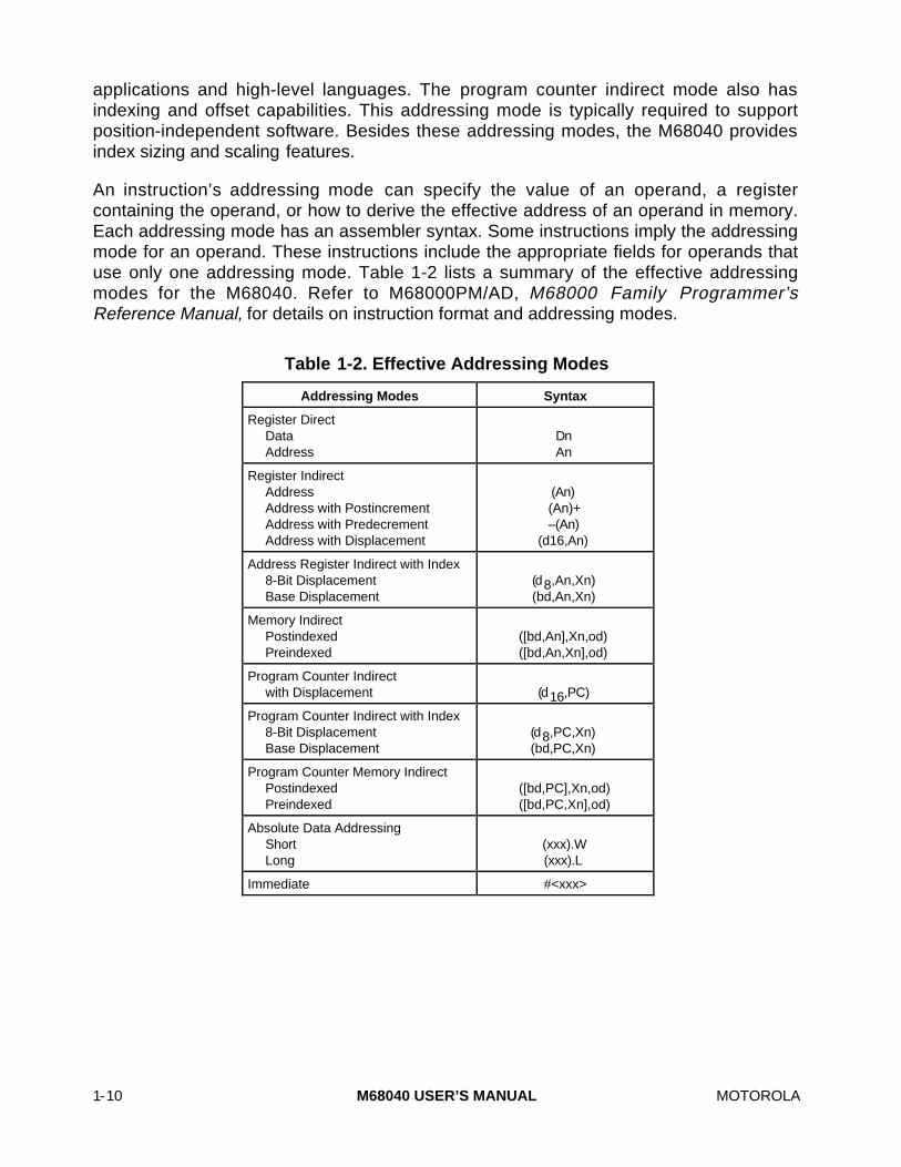
1-10 M68040 USER’S MANUAL MOTOROLA
applications and high-level languages. The program counter indirect mode also hasindexing and offset capabilities. This addressing mode is typically required to supportposition-independent software. Besides these addressing modes, the M68040 providesindex sizing and scaling features.
An instruction’s addressing mode can specify the value of an operand, a registercontaining the operand, or how to derive the effective address of an operand in memory.Each addressing mode has an assembler syntax. Some instructions imply the addressingmode for an operand. These instructions include the appropriate fields for operands thatuse only one addressing mode. Table 1-2 lists a summary of the effective addressingmodes for the M68040. Refer to M68000PM/AD, M68000 Family Programmer’sReference Manual, for details on instruction format and addressing modes.
Table 1-2. Effective Addressing Modes
Addressing Modes Syntax
Register DirectDataAddress
DnAn
Register IndirectAddressAddress with PostincrementAddress with PredecrementAddress with Displacement
(An)(An)+–(An)
(d16,An)
Address Register Indirect with Index8-Bit DisplacementBase Displacement
(d8,An,Xn)(bd,An,Xn)
Memory IndirectPostindexedPreindexed
([bd,An],Xn,od)([bd,An,Xn],od)
Program Counter Indirectwith Displacement (d16,PC)
Program Counter Indirect with Index8-Bit DisplacementBase Displacement
(d8,PC,Xn)(bd,PC,Xn)
Program Counter Memory IndirectPostindexedPreindexed
([bd,PC],Xn,od)([bd,PC,Xn],od)
Absolute Data AddressingShortLong
(xxx).W(xxx).L
Immediate #<xxx>

MOTOROLA M68040 USER’S MANUAL 1-11
1.9 NOTATIONAL CONVENTIONS
Table 1-3 lists the notation conventions used throughout this manual unless otherwisespecified.
Table 1-3. Notational Conventions
Single- And Double-Operand Operations
+ Arithmetic addition or postincrement indicator.
– Arithmetic subtraction or predecrement indicator.
× Arithmetic multiplication.
÷ Arithmetic division or conjunction symbol.
~ Invert; operand is logically complemented.
Λ Logical AND
V Logical OR
⊕ Logical exclusive OR
ø Source operand is moved to destination operand.
ł ø Two operands are exchanged.
<op> Any double-operand operation.
<operand>tested Operand is compared to zero and the condition codes are set appropriately.
sign-extended All bits of the upper portion are made equal to the high-order bit of the lower portion.
Other Operations
TRAP Equivalent to Format ÷ Offset Word ø (SSP); SSP – 2 ø SSP; PC ø (SSP); SSP – 4 ø SSP; SRø (SSP); SSP – 2 ø SSP; (Vector) ø PC
STOP Enter the stopped state, waiting for interrupts.
<operand>10 The operand is BCD; operations are performed in decimal.
If <condition>then <operations>
else <operations>
Test the condition. If true, the operations after “then” are performed. If the condition is falseand the optional “else” clause is present, the operations after “else” are performed. If thecondition is false and else is omitted, the instruction performs no operation. Refer to the Bccinstruction description as an example.
Register Specification
An Any Address Register n (example: A3 is address register 3)
Ax, Ay Source and destination address registers, respectively.
BR Base Register—An, PC, or suppressed.
Dc Data register D7–D0, used during compare.
Dh, Dl Data registers high- or low-order 32 bits of product.
Dn Any Data Register n (example: D5 is data register 5)
Dr, Dq Data register’s remainder or quotient of divide.
Du Data register D7–D0, used during update.
Dx, Dy Source and destination data registers, respectively.
MRn Any Memory Register n.
Rn Any Address or Data Register
Rx, Ry Any source and destination registers, respectively.
Xn Index Register—An, Dn, or suppressed.

1-12 M68040 USER’S MANUAL MOTOROLA
Table 1-3. Notational Conventions (Continued)
Data Format And Type
+ inf Positive Infinity
<fmt> Operand Data Format: Byte (B), Word (W), Long (L), Single (S), Double (D), Extended (X), orPacked (P).
B, W, L Specifies a signed integer data type (twos complement) of byte, word, or long word.
D Double-precision real data format (64 bits).
k A twos complement signed integer (–64 to +17) specifying a number’s format to be stored inthe packed decimal format.
P Packed BCD real data format (96 bits, 12 bytes).
S Single-precision real data format (32 bits).
X Extended-precision real data format (96 bits, 16 bits unused).
– inf Negative Infinity
Subfields and Qualifiers
#<xxx> or #<data> Immediate data following the instruction word(s).
( ) Identifies an indirect address in a register.
[ ] Identifies an indirect address in memory.
bd Base Displacement
ccc Index into the MC68881/MC68882 Constant ROM
dn Displacement Value, n Bits Wide (example: d16 is a 16-bit displacement).
LSB Least Significant Bit
LSW Least Significant Word
MSB Most Significant Bit
MSW Most Significant Word
od Outer Displacement
SCALE A scale factor (1, 2, 4, or 8, for no-word, word, long-word, or quad-word scaling, respectively).
SIZE The index register’s size (W for word, L for long word).
offset:width Bit field selection.
Register Names
CCR Condition Code Register (lower byte of status register)
DFC Destination Function Code Register
FPcr Any Floating-Point System Control Register (FPCR, FPSR, or FPIAR)
FPm, FPn Any Floating-Point Data Register specified as the source or destination, respectively.
IC, DC, IC/DC Instruction, Data, or Both Caches
MMUSR MMU Status Register
PC Program Counter
Rc Any Non Floating-Point Control Register
SFC Source Function Code Register
SR Status Register

MOTOROLA M68040 USER’S MANUAL 1-13
Table 1-3. Notational Conventions (Concluded)
Register Codes
* General Case.
C Carry Bit in CCR
cc Condition Codes from CCR
FC Function Code
N Negative Bit in CCR
U Undefined, Reserved for Motorola Use.
V Overflow Bit in CCR
X Extend Bit in CCR
Z Zero Bit in CCR
— Not Affected or Applicable.
Stack Pointers
ISP Supervisor/Interrupt Stack Pointer
MSP Supervisor/Master Stack Pointer
SP Active Stack Pointer
SSP Supervisor (Master or Interrupt) Stack Pointer
USP User Stack Pointer
Miscellaneous
<ea> Effective Address
<label> Assemble Program Label
<list> List of registers, for example D3–D0.
LB Lower Bound
m Bit m of an Operand
m–n Bits m through n of Operand
UB Upper Bound
1.10 INSTRUCTION SET OVERVIEW
The instruction set is tailored to support high-level languages and is optimized for thoseinstructions most commonly executed. The floating-point instructions for the M68040 are acommonly used subset of the MC68881/MC68882 instruction set with new arithmeticinstructions to explicitly select single- or double-precision rounding. The remainingunimplemented instructions are less frequently used and are efficiently emulated in theM68040FPSP, maintaining compatibility with the MC68881/MC68882 floating-pointcoprocessors. The M68040 instruction set includes MOVE16, a new user instruction thatallows high-speed transfers of 16-byte blocks between external devices such as memoryto memory or coprocessor to memory. Table 1-4 provides an alphabetized listing of theM68040 instruction set’s opcode, operation, and syntax. Refer to Table 1-3 for notationsused in Table 1-4. The left operand in the syntax is always the source operand, and theright operand is the destination operand. Refer to M68000PM/AD, M68000 FamilyProgrammer’s Reference Manual, for details on instructions used by the M68040.
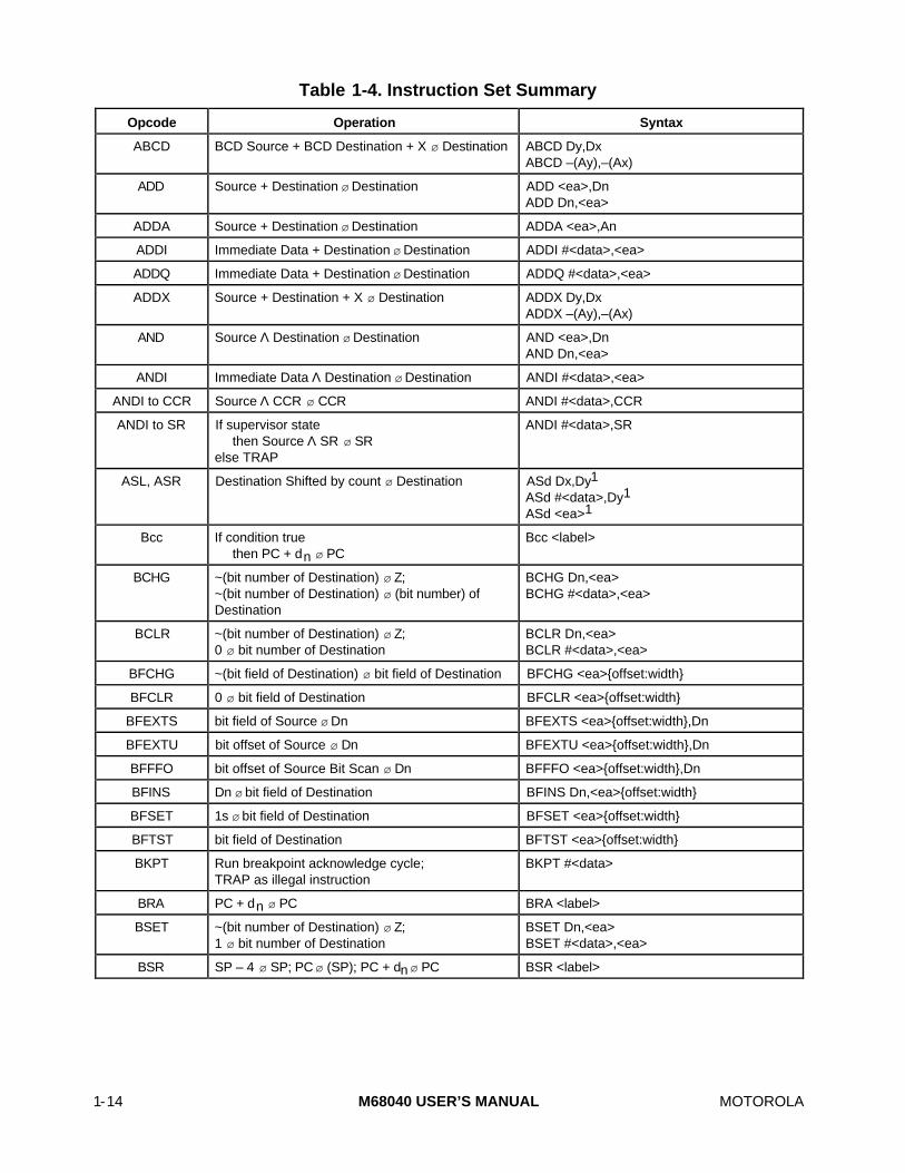
1-14 M68040 USER’S MANUAL MOTOROLA
Table 1-4. Instruction Set Summary
Opcode Operation Syntax
ABCD BCD Source + BCD Destination + X ø Destination ABCD Dy,DxABCD –(Ay),–(Ax)
ADD Source + Destination ø Destination ADD <ea>,DnADD Dn,<ea>
ADDA Source + Destination ø Destination ADDA <ea>,An
ADDI Immediate Data + Destination ø Destination ADDI #<data>,<ea>
ADDQ Immediate Data + Destination ø Destination ADDQ #<data>,<ea>
ADDX Source + Destination + X ø Destination ADDX Dy,DxADDX –(Ay),–(Ax)
AND Source Λ Destination ø Destination AND <ea>,DnAND Dn,<ea>
ANDI Immediate Data Λ Destination ø Destination ANDI #<data>,<ea>
ANDI to CCR Source Λ CCR ø CCR ANDI #<data>,CCR
ANDI to SR If supervisor statethen Source Λ SR ø SR
else TRAP
ANDI #<data>,SR
ASL, ASR Destination Shifted by count ø Destination ASd Dx,Dy1
ASd #<data>,Dy1
ASd <ea>1
Bcc If condition truethen PC + dn ø PC
Bcc <label>
BCHG ~(bit number of Destination) ø Z;~(bit number of Destination) ø (bit number) ofDestination
BCHG Dn,<ea>BCHG #<data>,<ea>
BCLR ~(bit number of Destination) ø Z;0 ø bit number of Destination
BCLR Dn,<ea>BCLR #<data>,<ea>
BFCHG ~(bit field of Destination) ø bit field of Destination BFCHG <ea>offset:width
BFCLR 0 ø bit field of Destination BFCLR <ea>offset:width
BFEXTS bit field of Source ø Dn BFEXTS <ea>offset:width,Dn
BFEXTU bit offset of Source ø Dn BFEXTU <ea>offset:width,Dn
BFFFO bit offset of Source Bit Scan ø Dn BFFFO <ea>offset:width,Dn
BFINS Dn ø bit field of Destination BFINS Dn,<ea>offset:width
BFSET 1s ø bit field of Destination BFSET <ea>offset:width
BFTST bit field of Destination BFTST <ea>offset:width
BKPT Run breakpoint acknowledge cycle;TRAP as illegal instruction
BKPT #<data>
BRA PC + dn ø PC BRA <label>
BSET ~(bit number of Destination) ø Z;1 ø bit number of Destination
BSET Dn,<ea>BSET #<data>,<ea>
BSR SP – 4 ø SP; PC ø (SP); PC + dn ø PC BSR <label>

MOTOROLA M68040 USER’S MANUAL 1-15
Table 1-4. Instruction Set Summary (Continued)
Opcode Operation Syntax
BTST –(bit number of Destination) ø Z; BTST Dn,<ea>BTST #<data>,<ea>
CAS CAS Destination – Compare Operand ø cc;if Z, Update Operand ø Destinationelse Destination ø Compare Operand
CAS Dc,Du,<ea>
CAS2 CAS2 Destination 1 – Compare 1 ø cc;if Z, Destination 2 – Compare ø cc;if Z, Update 1 ø Destination 1;
Update 2 ø Destination 2else Destination 1 ø Compare 1;
Destination 2 ø Compare 2
CAS2 Dc1–Dc2,Du1–Du2,(Rn1)–(Rn2)
CHK If Dn < 0 or Dn > Sourcethen TRAP
CHK <ea>,Dn
CHK2 If Rn < LB or If Rn > UBthen TRAP
CHK2 <ea>,Rn
CINV If supervisor statethen invalidate selected cache lines
else TRAP
CINVL <caches>, (An)CINVP <caches>, (An)CINVA <caches>
CLR 0 ø Destination CLR <ea>
CMP Destination – Source ø cc CMP <ea>,Dn
CMPA Destination – Source CMPA <ea>,An
CMPI Destination – Immediate Data CMPI #<data>,<ea>
CMPM Destination – Source ø cc CMPM (Ay)+,(Ax)+
CMP2 Compare Rn < LB or Rn > UBand Set Condition Codes
CMP2 <ea>,Rn
CPUSH If supervisor statethen if data cache push selected dirty datacache lines; invalidate selected cache lines
else TRAP
CPUSHL <caches>, (An)CPUSHP <caches>, (An)CPUSHA <caches>
DBcc If condition falsethen (Dn–1 ø Dn;
If Dn ≠ –1then PC + dn ø PC)
DBcc Dn,<label>
DIVS, DIVSL Destination ÷ Source ø Destination DIVS.W <ea>,Dn 32 ÷ 16 ø 16r:16qDIVS.L <ea>,Dq 32 ÷ 32 ø 32qDIVS.L <ea>,Dr:Dq 64 ÷ 32 ø 32r:32qDIVSL.L <ea>,Dr:Dq 32 ÷ 32 ø 32r:32q
DIVU, DIVUL Destination ÷ Source ø Destination DIVU.W <ea>,Dn 32 ÷ 16 ø 16r:16qDIVU.L <ea>,Dq 32 ÷ 32 ø 32qDIVU.L <ea>,Dr:Dq 64 ÷ 32 ø 32r:32qDIVUL.L <ea>,Dr:Dq 32 ÷ 32 ø 32r:32q
EOR Source ⊕ Destination ø Destination EOR Dn,<ea>
EORI Immediate Data ⊕ Destination ø Destination EORI #<data>,<ea>
EORI to CCR Source ⊕ CCR ø CCR EORI #<data>,CCR
EORI to SR If supervisor statethen Source ⊕ SR ø SR
else TRAP
EORI #<data>,SR

1-16 M68040 USER’S MANUAL MOTOROLA
Table 1-4. Instruction Set Summary (Continued)
Opcode Operation Syntax
EXG Rx ł ø Ry EXG Dx,DyEXG Ax,AyEXG Dx,AyEXG Ay,Dx
EXTEXTB
Destination Sign – Extended ø Destination EXT.W Dn extend byte to wordEXT.L L Dn extend word to long wordEXTB.L Dn extend byte to long word
FABS2 Absolute Value of Source ø FPn FABS.<fmt> <ea>,FPnFABS.X FPm,FPnFABS.X FPnFrABS.<fmt> <ea>,FPn3
FrABS.X FPm,FPn3
FrABS.X FPn3
FADD2 Source + FPn ø FPn FADD.<fmt> <ea>,FPnFADD.X FPm,FPnFrADD.<fmt> <ea>,FPn3
FrADD.X FPm,FPn3
FBcc2 If condition truethen PC + dn ø PC
FBcc.SIZE <label>
FCMP2FPn – Source FCMP.<fmt> <ea>,FPn
FCMP.X FPm,FPn
FDBcc2 If condition truethen no operation
else Dn – 1 ø Dnif Dn ≠ –1
then PC + dn ø PCelse execute next instruction
FDBcc Dn,<label>
FDIV2 FPn ÷ Source ø FPn FDIV.<fmt> <ea>,FPnFDIV.X FPm,FPnFrDIV.<fmt> <ea>,FPn3
FrDIV.X FPm,FPn3
FMOVE2 Source ø Destination FMOVE.<fmt> <ea>,FPnFMOVE.<fmt> FPM,<ea>FMOVE.P FPm,<ea>DnFMOVE.P FPm,<ea>#kFrMOVE.<fmt> <ea>,FPn3
FMOVE2Source ø Destination FMOVE.L <ea>,FPcr
FMOVE.L FPcr,<ea>
FMOVEM2 Register List ø DestinationSource ø Register List
FMOVEM.X <list>,<ea>4
FMOVEM.X Dn,<ea>FMOVEM.X <ea>,<list>4
FMOVEM.X <ea>,Dn
FMOVEM2 Register List ø DestinationSource ø Register List
FMOVEM.L <list>,<ea>5
FMOVEM.L <ea>,<list>5
FMUL2 Source × FPn ø FPn FMUL.<fmt> <ea>,FPnFMUL.X FPm,FPnFrMUL<fmt> <ea>,FPn3
FrMUL.X FPm,FPn3

MOTOROLA M68040 USER’S MANUAL 1-17
Table 1-4. Instruction Set Summary (Continued)
Opcode Operation Syntax
FNEG2 –(Source) ø FPn FNEG.<fmt> <ea>,FPnFNEG.X FPm,FPnFNEG.X FPnFrNEG.<fmt> <ea>,FPn3
FrNEG.X FPm,FPn3
FrNEG.X FPn3
FNOP2 None FNOP
FRESTORE2 If in supervisor statethen FPU State Frame ø Internal State
else TRAP
FRESTORE <ea>
FSAVE2 If in supervisor statethen FPU Internal State ø State Frame
else TRAP
FSAVE <ea>
FScc2 If condition truethen 1s ø Destination
else 0s ø Destination
FScc.SIZE <ea>
FSGLDIV FPn ÷ Source ø FPn FSGLDIV.<fmt> <ea>,FPnFSGLDIV.X FPm,FPn
FSGLMUL Source × FPn ø FPn FSGMUL.<fmt> <ea>,FPnFSGLMUL.X FPm, FPn
FSQRT2 Square Root of Source ø FPn FSQRT.<fmt> <ea>,FPnFSQRT.X FPm,FPnFSQRT.X FPnFrSQRT.<fmt> <ea>,FPn3
FrSQRT FPm,FPn3
FrSQRT FPn3
FSUB2 FPn – Source ø FPn FSUB.<fmt> <ea>,FPnFSUB.X FPm,FPnFrSUB.<fmt> <ea>,FPn3
FrSUB.X FPm,FPn3
FTRAPcc2 If condition truethen TRAP
FTRAPccFTRAPcc.W #<data>FTRAPcc.L #<data>
FTST2 Condition Codes for Operand ø FPCC FTST.<fmt> <ea>FTST.X FPm
ILLEGAL SSP – 2 ø SSP; Vector Offset ø (SSP);SSP – 4 ø SSP; PC ø (SSP);SSp – 2 ø SSP; SR ø (SSP);Illegal Instruction Vector Address ø PC
ILLEGAL
JMP Destination Address ø PC JMP <ea>
JSR SP – 4 ø SP; PC ø (SP)Destination Address ø PC
JSR <ea>
LEA <ea> ø An LEA <ea>,An
LINK SP – 4 ø SP; An ø (SP)SP ø An, SP+d ø SP
LINK An,dn

1-18 M68040 USER’S MANUAL MOTOROLA
Table 1-4. Instruction Set Summary (Continued)
Opcode Operation Syntax
LPSTOP6 If supervisor stateimmediate data ø SRSR ø broadcast cycleSTOP
else TRAP
LPSTOP #<data>
LSL, LSR Destination Shifted by count ø Destination LSd Dx,Dy1
LSd #<data>,Dy1
LSd <ea>1
MOVE Source ø Destination MOVE <ea>,<ea>
MOVEA Source ø Destination MOVEA <ea>,An
MOVEfrom CCR
CCR ø Destination MOVE CCR,<ea>
MOVE to CCR Source ø CCR MOVE <ea>,CCR
MOVE from SR If supervisor statethen SR ø Destination
else TRAP
MOVE SR,<ea>
MOVE to SR If supervisor statethen Source ø SR
else TRAP
MOVE <ea>,SR
MOVE USP If supervisor statethen USP ø An or An ø USP
else TRAP
MOVE USP,AnMOVE An,USP
MOVE16 Source block ø Destination block MOVE16 (Ax)+, (Ay)+7
MOVE16 (xxx).L, (An)MOVE16 (An), (xxx).LMOVE16 (An)+, (xxx).L
MOVEC If supervisor statethen Rc ø Rn or Rn ø Rc
else TRAP
MOVEC Rc,RnMOVEC Rn,Rc
MOVEM Registers ø DestinationSource ø Registers
MOVEM <list>,<ea>4
MOVEM <ea>,<list>4
MOVEP Source ø Destination MOVEP Dx,(dn,Ay)MOVEP (dn,Ay),Dx
MOVEQ Immediate Data ø Destination MOVEQ #<data>,Dn
MOVES If supervisor statethen Rn ø Destination [DFC] orSource [SFC] ø Rn
else TRAP
MOVES Rn,<ea>MOVES <ea>,Rn
MULS Source × Destination ø Destination MULS.W <ea>,Dn 16 × 16 ø 32MULS.L <ea>,Dl 32 × 32 ø 32MULS.L <ea>,Dh–Dl 32 × 32 ø 64
MULU Source × Destination ø Destination MULU.W <ea>,Dn 16 × 16 ø 32MULU.L <ea>,Dl 32 × 32 ø 32MULU.L <ea>,Dh–Dl 32 × 32 ø 64
NBCD 0 – (Destination10) – X ø Destination NBCD <ea>
NEG 0 – (Destination) ø Destination NEG <ea>
NEGX 0 – (Destination) – X ø Destination NEGX <ea>

MOTOROLA M68040 USER’S MANUAL 1-19
Table 1-4. Instruction Set Summary (Continued)
Opcode Operation Syntax
NOP None NOP
NOT ~ Destination ø Destination NOT <ea>
OR Source V Destination ø Destination OR <ea>,DnOR Dn,<ea>
ORI Immediate Data V Destination ø Destination ORI #<data>,<ea>
ORI to CCR Source V CCR ø CCR ORI #<data>,CCR
ORI to SR If supervisor statethen Source V SR ø SR
else TRAP
ORI #<data>,SR
PACK Source (Unpacked BCD) + adjustment øDestination (Packed BCD)
PACK –(Ax),–(Ay),#(adjustment)PACK Dx,Dy,#(adjustment)
PEA SP – 4 ø SP; <ea> ø (SP) PEA <ea>
PFLUSH8 If supervisor statethen invalidate instruction and data ATC entriesfor destination address
else TRAP
PFLUSH (An)PFLUSHN (An)PFLUSHAPFLUSHAN
PTEST8 If supervisor statethen logical address status ø MMUSR;entry ø ATC
else TRAP
PTESTR (An)PTESTW (An)
RESET If supervisor statethen Assert RSTO Line
else TRAP
RESET
ROL, ROR Destination Rotated by count ø Destination ROd Rx,Dy1
ROd #<data>,Dy1
ROXL, ROXR Destination Rotated with X by count ø Destination ROXd Dx,Dy1
ROXd #<data>,Dy1
ROXd <ea>1
RTD (SP) ø PC; SP + 4 + dn ø SP RTD #(dn)
RTE If supervisor statethen (SP) ø SR; SP + 2 ø SP; (SP) ø PC;SP + 4 ø SP; restore state and deallocatestack according to (SP)
else TRAP
RTE
RTR (SP) ø CCR; SP + 2 ø SP;(SP) ø PC; SP + 4 ø SP
RTR
RTS (SP) ø PC; SP + 4 ø SP RTS
SBCD Destination10 – Source10 – X ø Destination SBCD Dx,DySBCD –(Ax),–(Ay)
Scc If condition truethen 1s ø Destination
else 0s ø Destination
Scc <ea>
STOP If supervisor statethen Immediate Data ø SR; STOP
else TRAP
STOP #<data>
SUB Destination – Source ø Destination SUB <ea>,DnSUB Dn,<ea>

1-20 M68040 USER’S MANUAL MOTOROLA
Table 1-4. Instruction Set Summary (Concluded)
Opcode Operation Syntax
SUBA Destination – Source ø Destination SUBA <ea>,An
SUBI Destination – Immediate Data ø Destination SUBI #<data>,<ea>
SUBQ Destination – Immediate Data ø Destination SUBQ #<data>,<ea>
SUBX Destination – Source – X ø Destination SUBX Dx,DySUBX –(Ax),–(Ay)
SWAP Register 31–16 ¯ ø Register 15–0 SWAP Dn
TAS Destination Tested ø Condition Codes;1 ø bit 7 of Destination
TAS <ea>
TRAP SSP – 2 ø SSP; Format ÷ Offset ø (SSP);SSP – 4 ø SSP; PC ø (SSP); SSP – 2 ø SSP;SR ø (SSP); Vector Address ø PC
TRAP #<vector>
TRAPcc If ccthen TRAP
TRAPccTRAPcc.W #<data>TRAPcc.L #<data>
TRAPV If Vthen TRAP
TRAPV
TST Destination Tested ø Condition Codes TST <ea>
UNLK An ø SP; (SP) ø An; SP + 4 ø SP UNLK An
UNPK Source (Packed BCD) + adjustment ø Destination (Unpacked BCD)
UNPACK –(Ax),–(Ay),#(adjustment)UNPACK Dx,Dy,#(adjustment)
NOTES:1. Where d is direction, left or right.2. Available only on the MC68040.3. Where r is rounding precision, single or double precision.4. List refers to register.5. List refers to control registers only.6. Available only on the MC68040V and MC68EC040V.7. MOVE16 (ax)+,(ay)+ is functionally the same as MOVE16 (ax),(ay)+ when ax = ay. The address register is only
incremented once, and the line is copied over itself rather than to the next line.8. Not available for the MC68EC040 or MC68EC040V.

MOTOROLA M68040 USER’S MANUAL 2-1
SECTION 2INTEGER UNIT
This section describes the organization of the M68040 integer unit (IU) and presents abrief description of the associated registers. Refer to Section 3 Memory ManagementUnit (Except MC68EC040 and MC68EC040V) for details concerning the memorymanagement unit (MMU) programming model, and to Section 9 Floating-Point Unit(MC68040 Only) for details concerning the floating-point unit (FPU) programming model.
2.1 INTEGER UNIT PIPELINE
The IU carries out logical and arithmetic operations using six separate subunits. Each unitis dedicated to a different stage of the IU pipeline, handling a total of six separateinstructions simultaneously. Pipelining is a technique that overlaps the processing ofdifferent parts of several instructions. Pipelining simulates an assembly line with the IUcontaining a number of instructions in different phases of processing. The IU pipelineconsists of six stages:
1. Instruction Fetch—Fetching an instruction from memory.
2. Decode—Converting an instruction into micro-instructions.
3. <ea> Calculate—If the instruction calls for data from memory, the location of thedata, its memory address is calculated.
4. <ea> Fetch—Data is fetched from memory.
5. Execute—The data is manipulated during execution.
6. Write-Back—The result of the computation is written back to on-chip caches orexternal memory.
The pipeline contains special shadow registers that can begin processing futureinstructions for conditional branches while the main pipeline is processing currentinstructions. The <ea> calculate stage eliminates pipeline blockage for instructions withpostincrement, postdecrement, or immediate add and load to address register for updatesthat occur in the <ea> calculate stage. The write-back stage can write data over thesystem bus to store a result in external memory or directly to on-chip caches. These write-backs to memory can be deferred until the most opportune moment because of theM68040 bus interface. Figure 2-1 illustrates the IU pipeline.

2-2 M68040 USER’S MANUAL MOTOROLA
INSTRUCTION DATA FROM CACHE OR BUS
CONTROLLER
TO FPU
<ea> CALCULATE
<ea> FETCH TO CACHE OR BUS CONTROLLER
EXECUTE
WRITE-BACK
SHADOW
SHADOW
INSTRUCTION FETCH
DECODE
TO CACHE OR BUS CONTROLLER
Figure 2-1. Integer Unit Pipeline
An instruction stream is fetched from the instruction memory unit and decoded on aninstruction-by-instruction basis in the decode stage. Multiple instructions are fetched tokeep the pipeline stages full so that the pipeline will not stall.
The decoded instruction is then passed to the <ea> calculate stage to calculate theeffective addresses that the instruction requires. The <ea> calculate stage initiatesadditional fetches from the instruction stream to obtain the effective address extensionwords and performs the effective address calculation. The initial execution of theinstruction in the execute stage handles any data registers required for the calculation,which passes the register back to the <ea> calculate stage.
The resulting effective address is passed to the <ea> fetch stage, which initiates anoperand fetch from the data memory controller if the effective address is for a sourceoperand. The fetched operand is returned to the execute stage, which completesexecution of the instruction and writes any result to either a data register, memory, or backto the <ea> calculate stage for storage in an address register. For a memory destination,the <ea> fetch stage passes the address to the execution stage.
The previously described sequence of effective address calculation and fetch can occurmultiple times for an instruction, depending on the source and/or destination addressingmodes. For memory indirect addressing modes, the <ea> calculate stage initiates anoperand fetch from the intermediate indirect memory address, then calculates the final

MOTOROLA M68040 USER’S MANUAL 2-3
effective address. Also, some instructions access multiple memory operands and initiatefetches for each operand.
The instruction finishes execution in the execute stage. Instructions with write-backoperands to memory generate pending write accesses that are passed to the write-backstage. The write occurs to the data memory unit if it is not busy. If the following instruction,which is in the <ea> fetch stage, requires an operand fetch, the write-back stalls in thewrite-back stage since it is at a lower priority. The write-back can stall indefinitely untileither the data memory unit is free or another write is pending from the execution stage.
Figure 2-2 illustrates a write cycle, which begins in the IU pipeline. The IU stores thelogical address and data for a write operation in a temporary holding register (WB3). Writeoperation control passes from the IU to the data memory unit once the data memory unitis idle. When the data memory unit receives the logical address and data from the IU, itstores the logical address and data to a second temporary holding register (WB2). Thedata memory unit then translates the logical address into a physical address. If theaddress translation is successful, the data memory unit either stores an addresstranslation in the data cache (write hit) or passes it to the bus controller (write-through withwrite miss). Once the bus controller is ready to execute the external write operation, itmultiplexes the data to the correct data byte lanes and stores the multiplexed data andphysical address into a third holding register (WB1). WB1 is used in the actual writeoperation seen on the address and data buses. Appendix B MC68EC040 contains detailson address translation in the MC68EC040.
DECODE
<ea> CALCULATE
WRITE- BACK (WB3)
INTEGER UNIT
INSTRUCTION MEMORY UNIT
INSTRUCTION FETCH
EXECUTE
<ea> FETCH
ADDRESS BUS
DATA BUS
DATA CACHE
BUS CONTROLLER
WB1
DATA ATC
DATA MEMORY UNIT
DATA MMU/ CACHE/SNOOP CONTROLLER
WB2
DATA MUX
PUSH BUFFER
BUS CONTROL SIGNALS
LOG
ICAL
AD
DR
ESS
PHYSICAL ADDRESS
Figure 2-2. Write-Back Cycle Block Diagram
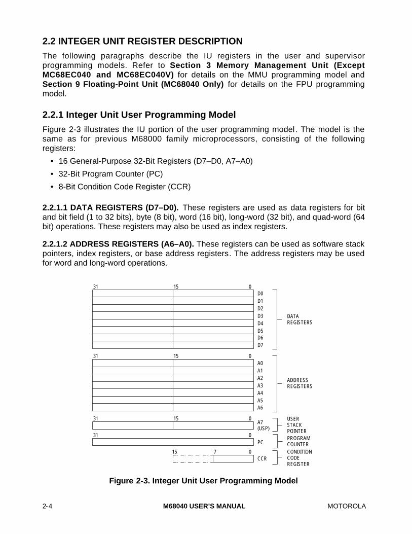
2-4 M68040 USER’S MANUAL MOTOROLA
2.2 INTEGER UNIT REGISTER DESCRIPTION
The following paragraphs describe the IU registers in the user and supervisorprogramming models. Refer to Section 3 Memory Management Unit (ExceptMC68EC040 and MC68EC040V) for details on the MMU programming model andSection 9 Floating-Point Unit (MC68040 Only) for details on the FPU programmingmodel.
2.2.1 Integer Unit User Programming Model
Figure 2-3 illustrates the IU portion of the user programming model. The model is thesame as for previous M68000 family microprocessors, consisting of the followingregisters:
• 16 General-Purpose 32-Bit Registers (D7–D0, A7–A0)
• 32-Bit Program Counter (PC)
• 8-Bit Condition Code Register (CCR)
2.2.1.1 DATA REGISTERS (D7–D0). These registers are used as data registers for bitand bit field (1 to 32 bits), byte (8 bit), word (16 bit), long-word (32 bit), and quad-word (64bit) operations. These registers may also be used as index registers.
2.2.1.2 ADDRESS REGISTERS (A6–A0). These registers can be used as software stackpointers, index registers, or base address registers. The address registers may be usedfor word and long-word operations.
A0A1A2A3A4A5A6
A7 (USP)
PC
D0D1D2D3D4D5D6D7
DATA REGISTERS
ADDRESS REGISTERS
USER STACK POINTERPROGRAM COUNTER
CCRCONDITION CODE REGISTER
01531
01531
0715
031
01531
Figure 2-3. Integer Unit User Programming Model
MOTOROLA M68040 USER’S MANUAL 2-5
2.2.1.3 SYSTEM STACK POINTER (A7). A7 is used as a hardware stack pointer duringstacking for subroutine calls and exception handling. The register designation A7 refers tothree different uses of the register: the user stack pointer (USP) (A7) in the userprogramming model and either the interrupt stack pointer (ISP) or master stack pointer(MSP) (A7' or A7", respectively) in the supervisor programming model. When the S-bit inthe status register (SR) is clear, the USP is the active stack pointer. Explicit references tothe system stack pointer (SSP) refer to the USP while the processor is operating in theuser mode.
A subroutine call saves the program counter (PC) on the active system stack, and thereturn restores it from the active system stack. Both the PC and the SR are saved on thesupervisor stack (either ISP or MSP) during the processing of exceptions and interrupts.Thus, the execution of supervisor level code is independent of user code and condition ofthe user stack. Conversely, user programs use the USP independently of supervisor stackrequirements.
2.2.1.4 PROGRAM COUNTER. The PC contains the address of the currently executinginstruction. During instruction execution and exception processing, the processorautomatically increments the contents of the PC or places a new value in the PC, asappropriate. For some addressing modes, the PC can be used as a pointer for PC-relativeaddressing.
2.2.1.5 CONDITION CODE REGISTER. The CCR consists of five bits of the SR leastsignificant byte. The first four bits represent a condition of the result generated by aprocessor operation. The fifth bit, the extend bit (X-bit), is an operand for multiprecisioncomputations. The carry bit (C-bit) and the X-bit are separate in the M68000 family tosimplify programming techniques that use them.
2.2.2 Integer Unit Supervisor Programming Model
Only system programmers use the supervisor programming model (see Figure 2-4) toimplement sensitive operating system functions, I/O control, and MMU subsystems. Allaccesses that affect the control features of the M68040 are in the supervisor programmingmodel. Thus, all application software is written to run in the user mode and migrates to theM68040 from any M68000 platform without modification.

2-6 M68040 USER’S MANUAL MOTOROLA
31 15 0
31 0
A7 '(ISP)
15 7 0
31 15A7 "(MSP)
031 2
31 0
SR
VBR
SFC
DFC
CACR
(CCR)
ALTERNATE SOURCE AND DESTINATION FUNCTION CODE REGISTERS
INTERRUPT STACK POINTER
MASTER STACK POINTER
STATUS REGISTER
VECTOR BASE REGISTER
CACHE CONTROL REGISTER
0
Figure 2-4. Integer Unit Supervisor Programming Model
The supervisor programming model consists of the registers available to the user as wellas the following control registers:
• Two 32-Bit Supervisor Stack Pointers (ISP, MSP)
• 16-Bit Status Register (SR)
• 32-Bit Vector Base Register (VBR)
• Two 32-Bit Alternate Function Code Registers: Source Function Code (SFC) andDestination Function Code (DFC)
• 32-Bit Cache Control Register (CACR)
The following paragraphs describe the supervisor programming model registers.Additional information on the ISP, MSP, SR, and VBR registers can be found in Section 8Exception Processing.
2.2.2.1 INTERRUPT AND MASTER STACK POINTERS. In a multitasking operatingsystem, it is more efficient to have a supervisor stack pointer associated with each usertask and a separate stack pointer for interrupt-associated tasks. The M68040 provides twosupervisor stack pointers, master and interrupt. Explicit references to the SSP refer toeither the MSP or ISP while the processor is operating in the supervisor mode. Allinstructions that use the SSP implicitly reference the active stack pointer. The ISP andMSP are general-purpose registers and can be used as software stack pointers, indexregisters, or base address registers. The ISP and MSP can be used for word and long-word operations.
The M-bit of the SR selects whether the ISP or MSP is active. SSP references access theISP when the M-bit is clear, putting the processor into the interrupt mode. If an exceptionbeing processed is an interrupt and the M-bit is set, the M-bit is cleared, putting theprocessor into the interrupt mode. The interrupt mode is the default condition after reset,and all SSP references access the ISP. The ISP can be used for interrupt controlinformation and for workspace area as interrupt exception handling requires.
SSP references access the MSP when the M-bit is set. The operating system uses theMSP for each task pointing to a task-related area of supervisor data space. This

MOTOROLA M68040 USER’S MANUAL 2-7
procedure separates task-related supervisor activity from asynchronous, I/O-relatedsupervisor tasks that can only be coincidental to the currently executing task. The MSPcan separately maintain task control information for each currently executing user task,and the software updates the MSP when a task switch is performed, providing an efficientmeans for transferring task-related stack items. The value of the M-bit does not affectexecution of privileged instructions. Instructions that affect the M-bit are MOVE to SR,ANDI to SR, EORI to SR, ORI to SR, and RTE. The processor automatically saves the M-bit value and clears it in the SR as part of the exception processing for interrupts.
2.2.2.2 STATUS REGISTER. The SR (see Figure 2-5) stores the processor status. In thesupervisor mode, software can access the full SR, including the CCR available in usermode (see 2.2.1.5 Condition Code Register) and the interrupt priority mask andadditional control bits available only in the supervisor mode. These bits indicate thefollowing states for the processor: one of two trace modes (T1, T0), supervisor or usermode (S), and master or interrupt mode (M).
The term SSP refers to the ISP and MSP. The M and S bits of the SR decide which SSPto use. When the S-bit is one and the M-bit is zero, the ISP is the active stack pointer;when the S-bit is one and the M-bit is one, the MSP is the active stack pointer. The ISP isthe default mode after reset and corresponds to the MC68000, MC68008, MC68010, andCPU32 supervisor mode.
T1 T0 S M 0 I2 I1 I0 X N Z V C0 0 0
SYSTEM BYTEUSER BYTE
(CONDITION CODE REGISTER)
TRACE ENABLE
INTERRUPT PRIORITY MASK
SUPERVISOR/USER STATE
MASTER/INTERRUPT STATE EXTEND
NEGATIVE
ZERO
OVERFLOW
CARRY
15 14 13 12 11 10 9 8 7 56 4 3 2 1 0
Figure 2-5. Status Register
2.2.2.3 VECTOR BASE REGISTER. The VBR contains the base address of the exceptionvector table in memory. The displacement of an exception vector is added to the value inthis register to access the vector table. Refer to Section 8 Exception Processing forinformation on exception vectors.
2.2.2.4 ALTERNATE FUNCTION CODE REGISTERS. The alternate function coderegisters contain 3-bit function codes. Function codes can be considered extensions of the32-bit logical address that optionally provides as many as eight 4-Gbyte address spaces.The processor automatically generates function codes to select address spaces for dataand programs at the user and supervisor modes. Certain instructions use the SFC andDFC registers to specify the function codes for operations.

2-8 M68040 USER’S MANUAL MOTOROLA
2.2.2.5 CACHE CONTROL REGISTER. The CACR contains two enable bits that allowthe instruction and data caches to be independently enabled or disabled. Setting anenable bit enables the associated cache without affecting the state of any lines within thecache. A hardware reset clears the CACR, disabling both caches.
MOTOROLA M68040 USER'S MANUAL 3-1
SECTION 3MEMORY MANAGEMENT UNIT(EXCEPT MC68EC040 AND MC68EC040V)
NOTE
This section does not apply to the MC68EC040 andMC68EC040V. Refer to Appendix B MC68EC040 for details.All references to M68040 in this section only, refer to theMC68040, MC68040V, and MC68LC040.
The M68040 supports a demand-paged virtual memory environment. Demand means thatprograms request memory accesses through logical addresses, and paged means thatmemory is divided into blocks of equal size, called page frames. Each page frame isdivided into pages of the same size. The operating system assigns pages to page framesas they are required to meet the needs of the program.
The M68040 memory management includes the following features:
• Independent Instruction and Data Memory Management Units (MMUs)
• 32-Bit Logical Address Translation to 32-Bit Physical Address
• User-Defined 2-Bit Physical Address Extension
• Addresses Translated in Parallel with Indexing into Data or Instruction Cache
• 64-Entry Four-Way Set-Associative Address Translation Cache (ATC) for Each MMU(128 Total Entries)
• Global Bit Allowing Flushes of All Nonglobal Entries from ATCs
• Selectable 4K or 8K Page Size
• Separate Supervisor and User Translation tables
• Two Independent Blocks for Each MMU Can Be Defined as Transparent(Untranslated)
• Three-Level Translation Tables with Optional Indirection
• Supervisor and Write Protections
• History Bits Automatically Maintained in Descriptors
• External Translation Disable Input Signal (MDIS) for Emulator Support
• Caching Mode Selected on Page Basis
The MMUs completely overlap address translation time with other processing activitieswhen the translation is resident in one of the ATCs. ATC accesses operate in parallel with

3-2 M68040 USER'S MANUAL MOTOROLA
indexing into the on-chip instruction and data caches. The MMU MDIS signal dynamicallydisables address translation for emulation and diagnostic support.
Figure 3-1 illustrates the MMUs contained in the two memory units, one for instructions(supporting instruction prefetches) and one for data (supporting all other accesses). Eachunit contains an MMU, main cache, and snoop controller. The corresponding MMUscontain two transparent translation registers, which identify blocks of memory that can beaccessed without translation. The MMUs also contain control logic and correspondingaddress translation caches (ATCs) in which recently used logical-to-physical addresstranslations are stored. The data memory unit contains a data write and data read buffer,and the instruction memory unit contains an instruction line read buffer. These bufferstemporarily hold data until an opportune moment arises to write the data to externalmemory or read the operand/instruction into the integer unit.
INSTRUCTION FETCH
DECODE
EA CALCULATE
EXECUTE
WRITE- BACK
EA FETCH
INTEGER UNIT
CONVERT
EXECUTE
WRITE- BACK
INSTRUCTION ATC
INSTRUCTION MMU/CACHE/SNOOP
CONTROLLER
BUS CONTROL SIGNALS
DATA BUS
ADDRESS BUS
DATA ATC
DATA MMU/CACHE/SNOOP
CONTROLLER
OPERAND DATA BUS
INSTRUCTION DATA BUS
INSTRUCTION CACHE
DATA CACHE
FLOATING- POINT UNIT
DATA MEMORY UNIT
INSTRUCTION MEMORY UNIT B U S
C O N T R O L L E R
INSTRUCTION ADDRESS
DATA ADDRESS
Figure 3-1. Memory Management Unit
The principal MMU function is to translate logical addresses to physical addresses usingtranslation tables stored in memory. As the MMU receives a logical address from theinteger unit, it searches its ATC for the corresponding physical address using the upper

MOTOROLA M68040 USER'S MANUAL 3-3
logical address bits. If the translation is resident, the MMU provides the physical addressto the cache controller, which determines if the instruction or data being accessed iscached. The cache controller uses the lower address bits to index into memory. Anexternal bus cycle is performed only when explicitly requested by the cache controller.When the translation is not in the ATC, the MMU searches the translation tables inmemory for the translation information. Microcode and dedicated logic perform theaddress calculations and bus cycles required for this search.
3.1 MEMORY MANAGEMENT PROGRAMMING MODEL
The memory management programming model is part of the supervisor programmingmodel for the M68040. The eight registers that control and provide status information foraddress translation in the M68040 are: the user root pointer register (URP), the supervisorroot pointer register (SRP), the translation control register (TCR), four independenttransparent translation registers (ITT0, ITT1, DTT0, and DTT1), and the MMU statusregister (MMUSR). Only programs that execute in the supervisor mode can directlyaccess these registers. Figure 3-2 illustrates the memory management programmingmodel.
31 0
31 0
31 0
0
31 0
31 0
31 0
31 0
URP
SRP
TCR
DTTR0
ITTR0
DTTR1
ITTR1
MMUSR
15
DATA TRANSPARENT TRANSLATION REGISTER 0
USER ROOT POINTER REGISTER
SUPERVISOR ROOT POINTER REGISTER
TRANSLATION CONTROL REGISTER
INSTRUCTION TRANSPARENT TRANSLATION REGISTER 0
MMU STATUS REGISTER
INSTRUCTION TRANSPARENT TRANSLATION REGISTER 1
DATA TRANSPARENT TRANSLATION REGISTER 1
Figure 3-2. Memory Management Programming Model
3.1.1 User and Supervisor Root Pointer Registers
The SRP and URP registers each contain the physical address of the translation table’sroot, which the MMU uses for supervisor and user accesses, respectively. The URP pointsto the translation table for the current user task. When a new task begins execution, theoperating system typically writes a new root pointer to the URP. A new translation tableaddress implies that the contents of the ATCs may no longer be valid. A PFLUSHinstruction should be executed to flush the ATCs before loading a new root pointer value,if necessary. Figure 3-3 illustrates the format of the 32-bit URP and SRP registers. Bits 8–

3-4 M68040 USER'S MANUAL MOTOROLA
0 of an address loaded into the URP or the SRP must be zero. Transfers of data to andfrom these 32-bit registers are long-word transfers.
31 9 8 0
USER ROOT POINTER 0 0 0 0 0 0 0 0 0
SUPERVISOR ROOT POINTER 0 0 0 0 0 0 0 0 0
Figure 3-3. URP and SRP Register Formats
3.1.2 Translation Control Register
The 16-bit TCR contains two control bits to enable paged address translation and to selectpage size. The operating system must flush the ATCs before enabling address translationsince the TCR accesses and reset do not flush the ATCs. All unimplemented bits of thisregister are read as zeros and must always be written as zeros. The M68040 always usesword transfers to access this 16-bit register. The fields of the TCRs are defined followingFigure 3-4, which illustrates the TCR.
15 14 13 12 11 10 9 8 7 6 5 4 3 2 1 0
E P 0 0 0 0 0 0 0 0 0 0 0 0 0 0
NOTE: Bits 13–0 are undefined (reserved).
Figure 3-4. Translation Control Register Format
E—EnableThis bit enables and disables paged address translation.
0 = Disable1 = Enable
A reset operation clears this bit. When translation is disabled, logical addresses areused as physical addresses. The MMU instruction, PFLUSH, can be executedsuccessfully despite the state of the E-bit. PTEST results are undefined if the MMU isdisabled and no table search occurs. If translation is disabled and an access does notmatch a transparent translation register (TTR), the access has the following defaultattributes on the TTR: the caching mode is cachable/write-through, write protection isdisabled, and the user attribute signals (UPA1 and UPA0) are zero.
P—Page SizeThis bit selects the memory page size.
0 = 4 Kbytes1 = 8 Kbytes
A reset operation does not affect this bit. The bit must be initialized after a reset.
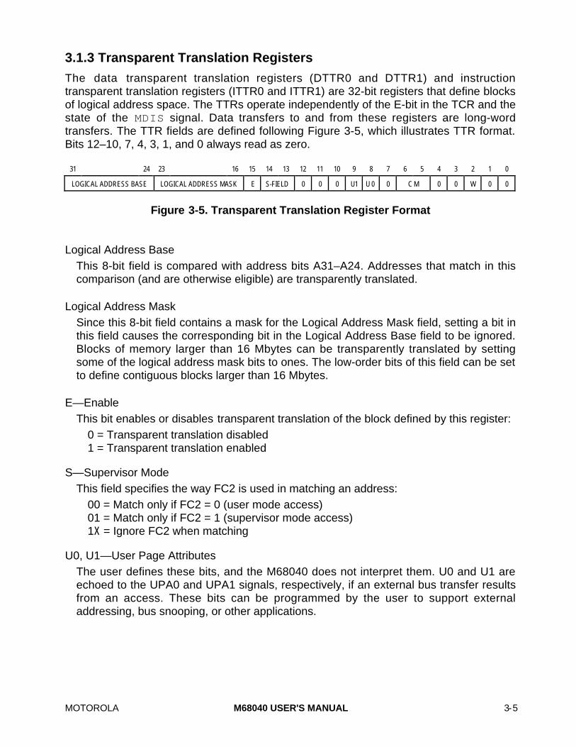
MOTOROLA M68040 USER'S MANUAL 3-5
3.1.3 Transparent Translation Registers
The data transparent translation registers (DTTR0 and DTTR1) and instructiontransparent translation registers (ITTR0 and ITTR1) are 32-bit registers that define blocksof logical address space. The TTRs operate independently of the E-bit in the TCR and thestate of the MDIS signal. Data transfers to and from these registers are long-wordtransfers. The TTR fields are defined following Figure 3-5, which illustrates TTR format.Bits 12–10, 7, 4, 3, 1, and 0 always read as zero.
31 24 23 16 15 14 13 12 11 10 9 8 7 6 5 4 3 2 1 0
LOGICAL ADDRESS BASE LOGICAL ADDRESS MASK E S-FIELD 0 0 0 U1 U 0 0 C M 0 0 W 0 0
Figure 3-5. Transparent Translation Register Format
Logical Address BaseThis 8-bit field is compared with address bits A31–A24. Addresses that match in thiscomparison (and are otherwise eligible) are transparently translated.
Logical Address MaskSince this 8-bit field contains a mask for the Logical Address Mask field, setting a bit inthis field causes the corresponding bit in the Logical Address Base field to be ignored.Blocks of memory larger than 16 Mbytes can be transparently translated by settingsome of the logical address mask bits to ones. The low-order bits of this field can be setto define contiguous blocks larger than 16 Mbytes.
E—EnableThis bit enables or disables transparent translation of the block defined by this register:
0 = Transparent translation disabled1 = Transparent translation enabled
S—Supervisor ModeThis field specifies the way FC2 is used in matching an address:
00 = Match only if FC2 = 0 (user mode access)01 = Match only if FC2 = 1 (supervisor mode access)1X = Ignore FC2 when matching
U0, U1—User Page AttributesThe user defines these bits, and the M68040 does not interpret them. U0 and U1 areechoed to the UPA0 and UPA1 signals, respectively, if an external bus transfer resultsfrom an access. These bits can be programmed by the user to support externaladdressing, bus snooping, or other applications.
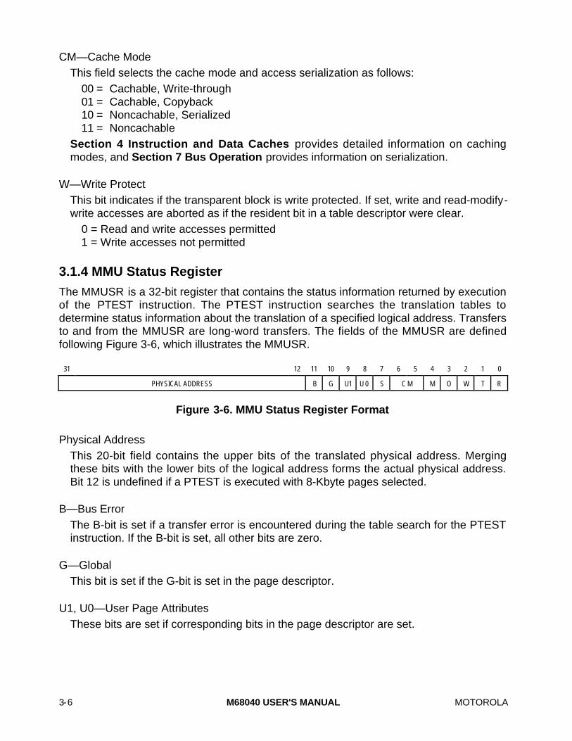
3-6 M68040 USER'S MANUAL MOTOROLA
CM—Cache ModeThis field selects the cache mode and access serialization as follows:
00 = Cachable, Write-through01 = Cachable, Copyback10 = Noncachable, Serialized11 = Noncachable
Section 4 Instruction and Data Caches provides detailed information on cachingmodes, and Section 7 Bus Operation provides information on serialization.
W—Write ProtectThis bit indicates if the transparent block is write protected. If set, write and read-modify-write accesses are aborted as if the resident bit in a table descriptor were clear.
0 = Read and write accesses permitted1 = Write accesses not permitted
3.1.4 MMU Status Register
The MMUSR is a 32-bit register that contains the status information returned by executionof the PTEST instruction. The PTEST instruction searches the translation tables todetermine status information about the translation of a specified logical address. Transfersto and from the MMUSR are long-word transfers. The fields of the MMUSR are definedfollowing Figure 3-6, which illustrates the MMUSR.
31 12 11 10 9 8 7 6 5 4 3 2 1 0
PHYSICAL ADDRESS B G U1 U 0 S C M M O W T R
Figure 3-6. MMU Status Register Format
Physical AddressThis 20-bit field contains the upper bits of the translated physical address. Mergingthese bits with the lower bits of the logical address forms the actual physical address.Bit 12 is undefined if a PTEST is executed with 8-Kbyte pages selected.
B—Bus ErrorThe B-bit is set if a transfer error is encountered during the table search for the PTESTinstruction. If the B-bit is set, all other bits are zero.
G—GlobalThis bit is set if the G-bit is set in the page descriptor.
U1, U0—User Page AttributesThese bits are set if corresponding bits in the page descriptor are set.

MOTOROLA M68040 USER'S MANUAL 3-7
S—Supervisor ProtectionThis bit is set if the S-bit in the page descriptor is set. Setting this bit does not indicatethat a violation has occurred.
CM—Cache ModeThis 2-bit field is copied from the CM bits in the page descriptor.
M—ModifiedThis bit is set if the M-bit is set in the page descriptor associated with the address.
W—Write ProtectThis bit is set if the W-bit is set in any of the descriptors encountered during the tablesearch. Setting this bit does not indicate that a violation has occurred.
T—Transparent Translation Register HitIf the T-bit is set, then the PTEST address matches an instruction or data TTR, the R-bitis set, and all other bits are zero.
R—ResidentThe R-bit is set if the PTEST address matches an instruction or data TTR or if the tablesearch completes by obtaining a valid page descriptor.
3.2 LOGICAL ADDRESS TRANSLATION
The function of the MMUs is to translate logical addresses to physical addresses. TheMMUs perform translations according to control information in translation tables. Theoperating system creates these translation tables and stores them in memory. Theprocessor then fetches a translation table as needed and stores it in an ATC.
3.2.1 Translation Tables
The M68040 uses the ATCs in the instruction and data memory units with translationtables stored in memory to perform the translations from logical to physical addresses.The operating system loads the translation tables for a program into memory. Nodistinction is made in the translation of instruction accesses versus data accessesbecause the instruction and data MMUs access the same translation table for a specificprivilege mode, either user or supervisor. This lack of distinction results in a mergedinstruction and data address space.
Figure 3-7 illustrates the three-level tree structure of a general translation table supportedby the M68040. The root- and pointer-level tables contain the base addresses of thetables at the next level. The page-level tables contain either the physical address for thetranslation or a pointer to the memory location containing the physical address. Only aportion of the translation table for the entire logical address space is required to beresident in memory at any time—specifically, only the portion of the table that translates

3-8 M68040 USER'S MANUAL MOTOROLA
the logical addresses of the currently executing process. Portions of translation tables canbe dynamically allocated as the process requires additional memory.
ROOT POINTER
PAGE TABLES
FIRST LEVEL
SECOND LEVEL
THIRD LEVEL
POINTER TABLES
ROOT TABLES
Figure 3-7. Translation Table Structure
The current privilege mode determines the use of the URP or SRP for translation of theaccess. The root pointer contains the base address of the translation table’s root-leveltable. The translation table consists of tables of descriptors. The table descriptors of theroot- and pointer-levels can be either resident or invalid. The page descriptors of the page-level table can be resident, indirect, or invalid. A page descriptor defines the physicaladdress of a page frame in memory that corresponds to the logical address of a page. Anindirect descriptor, which contains a pointer to the actual page descriptor, can be usedwhen two or more logical addresses access a single page descriptor.
The table search uses logical addresses to access the translation tables. Figure 3-8illustrates a logical address format, which is segmented into four fields: root index (RI),pointer index (PI), page index (PGI), and page offset. The first three fields extracted fromthe logical address index the base address for each table level. The seven bits of thelogical address RI field are multiplied by 4 or shifted to the left by two bits. This sum isconcatenated with the upper 23 bits of the appropriate root pointer (URP or SRP) to yieldthe physical address of a root-level table descriptor. Each of the 128 root-level tabledescriptors corresponds to a 32-Mbyte block of memory and points to the base of apointer-level table.

MOTOROLA M68040 USER'S MANUAL 3-9
7 BITS
31 25 24 18 17 13 12 11 0
7 BITS8K PAGE 4K PAGE
8K PAGE 4K PAGE
ROOT INDEX FIELD (RI)
POINTER INDEX FIELD (PI)
PAGE INDEX FIELD (PGI)
PAGE OFFSET
Figure 3-8. Logical Address Format
The seven bits of a logical address PI field are multiplied by 4 (shifted to the left by twobits) and concatenated with the fetched root-level descriptor’s upper 23 bits to produce thephysical address of the pointer-level table descriptor. Each of the 128 pointer-level tabledescriptors corresponds to a 256-Kbyte block of memory.
For 8-Kbyte pages, the five bits of the PGI field are multiplied by 4 (shifted to the left bytwo bits) and concatenated with the fetched pointer-level descriptor’s upper 25 bits toproduce the physical address of the 8-Kbyte page descriptor. The upper 19 bits of thepage descriptor are the page frame’s physical address. There are 32 8-Kbyte pagedescriptors in a page-level table.
Similarly, for 4-Kbyte pages, the six bits of the PGI field are multiplied by 4 (shifted to theleft by two bits) and concatenated with the fetched pointer-level descriptor’s upper 24 bitsto produce the physical address of the 4-Kbyte page descriptor. The upper 20 bits of thepage descriptor are the page frame’s physical address. There are 64 4-Kbyte pagedescriptors in a page-level table.
Write-protect status is accumulated from each level’s descriptor and combined with thestatus from the page descriptor to form the ATC entry status. The M68040 creates theATC entry from the page frame address and the associated status bits and retries theoriginal bus access. Refer to 3.3 Address Translation Caches for details on ATC entries.
If the descriptor from a page table is an indirect descriptor, the page descriptor pointed toby this descriptor is fetched. Invalid descriptors can be used at any level of the tree exceptthe root. When a table search for a normal translation encounters an invalid descriptor, theprocessor takes an access fault exception. The invalid descriptor can be used to identifyeither a page or branch of the tree that has been stored on an external device and is notresident in memory or a portion of the translation table that has not yet been defined. Inthese two cases, the exception routine can either restore the page from disk or add to thetranslation table. Figures 3-9 and 3-10 illustrate detailed flowcharts of table search anddescriptor fetch operations.
A table search terminates successfully when a page descriptor is encountered. Theoccurrence of an invalid descriptor or a transfer error acknowledge also terminates a tablesearch, and the M68040 takes an exception on the retry of the cycle because of theseconditions. The exception handler should distinguish between anticipated conditions andtrue error conditions. The exception handler can correct an invalid descriptor that indicatesa nonresident page or one that identifies a portion of the translation table yet to beallocated. An access error due to a system malfunction can require the exception handlerto write an error message and terminate the task.

3-10 M68040 USER'S MANUAL MOTOROLA
ENTRY
SELECT ROOT POINTERFC2 = 0:URP, 1:SRP
FETCH ROOT DESCRIPTOR
FETCH POINTER DESCRIPTOR
FETCH PAGE DESCRIPTOR
TYPE 'INDIRECT'
FETCH INDIRECT DESCRIPTOR
EXIT TABLE SEARCH
CREATE ATC ENTRYWITH R-BIT CLEAR
EXIT TABLE SEARCH
(INITIALIZE ACCRUED STATUS)
CREATE ATC ENTRY WITH R-BIT SET
ATC ENTRY PFA, DF[U1,U0,S,CM,M],WPATC TAG FC2, LA, DF[G]
ABBREVIATIONS:
PFA - PAGE FRAME ADDRESSDF[ ] - DESCRIPTOR FIELDWP - ACCUMULATED WRITE- PROTECTION STATUS ASSIGNMENT OPERATOR
WP 0
TYPE 'POINTER'UPDATE FALSE
TYPE 'PAGE'
'RESIDENT' 'INVALID'
'RESIDENT'
'INVALID' 'RESIDENT'
'RESIDENT'OTHERWISE
'INDIRECT'
PFA = PHYSICAL ADDRESSFIELD OF DESCRIPTOR
'INVALID'
(CHECK DESCRIPTOR TYPE)
(CHECK DESCRIPTOR TYPE)
(CHECK DESCRIPTOR TYPE)
(CHECK DESCRIPTOR TYPE)
Figure 3-9. Detailed Flowchart of Table Search Operation

MOTOROLA M68040 USER'S MANUAL 3-11
CREATE ATC ENTRYWITH R-BIT CLEAR
FETCH DESCRIPTOR &UPDATE HISTORY AND STATUS
FETCH DESCRIPTORAT PA = TA + (INDEX*4)
FETCH DESCRIPTOR ATPA = DESCRIPTOR ADDRESS
WP = WP V W
OR 'INDIRECT'
EXECUTEWRITE ACCESS
U 1, M 1
EXECUTELOCKED
RMW ACCESSU 1
U = 1 &U = 0 &
SCHEDULEWRITE ACCESS
U 1(SEE NOTE)
WP = WP V W
IF SCHEDULED, EXECUTEWRITE ACCESS (U 1) FOR
PREVIOUS DESCRIPTOR
CREATE ATC ENTRYWITH R-BIT CLEAR
WP – ACCUMULATED WRITE- PROTECTION STATUSV – LOGICAL "OR" OPERATOR – ASSIGNMENT OPERATOR
DUE TO ACCESS PIPELINING, A POINTERDESCRIPTOR WRITE ACCESS TO UPDATETHE U-BIT OCCURS AFTER THE READ OFTHE NEXT LEVEL DESCRIPTOR.
NOTE :
ABBREVIATIONS:
RETURNRETURN
RETURN
RETURN EXIT TABLE SEARCH
EXIT TABLE SEARCH
TYPE = 'PAGE' OR 'POINTER'
OTHERWISE
TYPE = 'PAGE'
'INVALID'
'RESIDENT''RESIDENT'
U = 1U = 0
'INVALID'
TYPE ='POINTER'
READ ACCESS
U = 0 (WP = 1 OR M = 1) (WP = 1 OR M = 1)
WP = 0 & M = 0U = 1
WRITE ACCESS
OTHERWISE
TYPE = 'INDIRECT'
(INDEX = RI, PI, OR PGI)
(SEE NOTE)
NORMAL TERMINATIONOF ALL BUS TRANSFERS
NORMAL TERMINATIONOF ALL BUS TRANSFERS
OR 'INDIRECT'
Figure 3-10. Detailed Flowchart of Descriptor Fetch Operation
3-12 M68040 USER'S MANUAL MOTOROLA
Motorola highly recommends that the translation tables be placed in cache-inhibitedmemory space. Motorola also highly recommends table descriptors must not be left instates that are incoherent to the processor. Future processors may treat theserecommendations as mandatory. The following paragraphs apply only to M68040 systemsthat cannot meet these recommendations.
The processor never allocates table descriptors in the data cache when the processorperforms a table search. Only normal accesses to the translation tables cause descriptorsto be allocated in the data cache. If table descriptors are allocated in the data cache andthe cache is disabled, the processor locks up trying to access a cached descriptor duringa table search. Ensuring that the data cache is invalidated before enabling the MMU ordisabling the data cache and ensuring that the pages containing table descriptors arepushed and invalidated prevents lockup during table searches.
Table and page descriptors must not be left in a state that is incoherent to the processor.Violation of this restriction can result in an undefined operation. Page descriptors must nothave an encoding of U-bit = 0, M-bit = 1 and PDT field = 01 or 11. This encoding indicatesthat the page descriptor is resident, not used, and modified. The processor’s table searchalgorithm never leaves a descriptor in this state. This state is possible through directmanipulation by the operating system for this specific instance. A table search for aMOVE16 write can corrupt the cache line being written if the table descriptors are markedcopyback.
3.2.2 Descriptors
There are two types of descriptors used in the translation tables, table and page. Table-and page-level descriptors can be further divided into types of descriptors. Root tabledescriptors are used in root-level tables and pointer table descriptors are used in pointer-level tables. Descriptors in the page-level tables contain either a page descriptor for thetranslation or an indirect descriptor that points to a memory location containing the pagedescriptor. The P-bit in the TCR selects the page size as either 4 or 8 Kbytes.
3.2.2.1 TABLE DESCRIPTORS. Figure 3-11 illustrates the formats of the root and pointertable descriptors. Two descriptor formats are possible at the pointer-level tables to support4-Kbyte and 8-Kbyte page sizes.
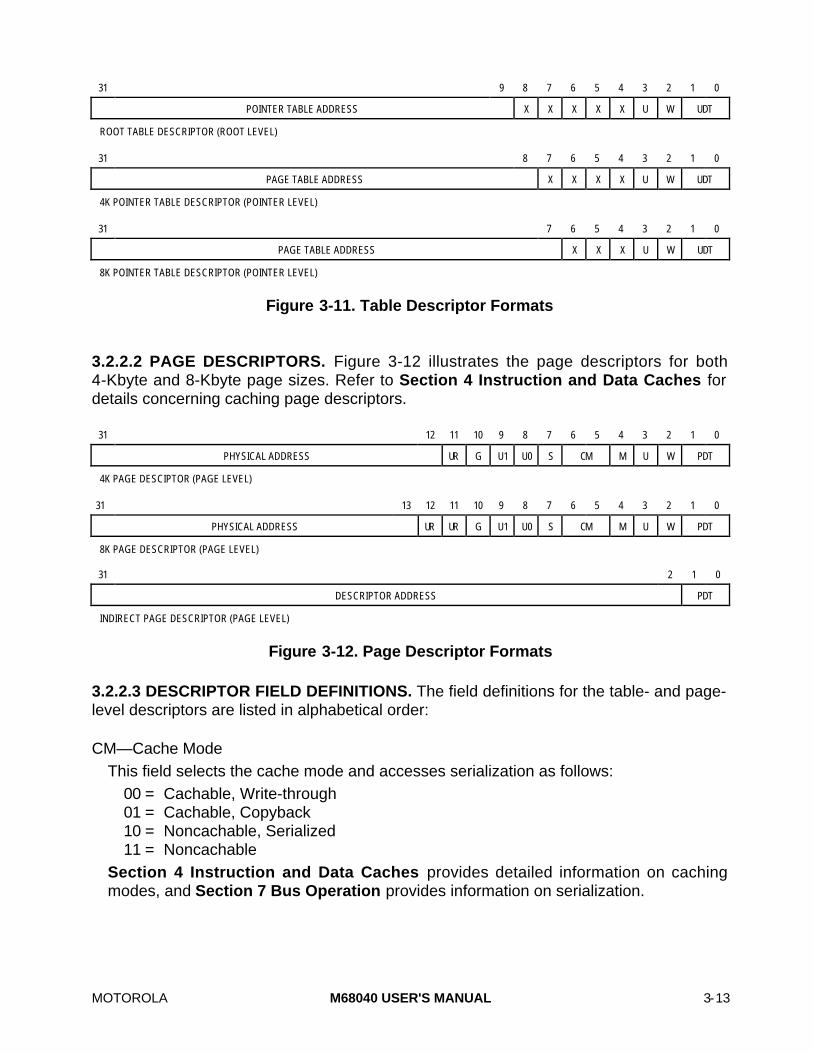
MOTOROLA M68040 USER'S MANUAL 3-13
31 9 8 7 6 5 4 3 2 1 0
POINTER TABLE ADDRESS X X X X X U W UDT
ROOT TABLE DESCRIPTOR (ROOT LEVEL)
31 8 7 6 5 4 3 2 1 0
PAGE TABLE ADDRESS X X X X U W UDT
4K POINTER TABLE DESCRIPTOR (POINTER LEVEL)
31 7 6 5 4 3 2 1 0
PAGE TABLE ADDRESS X X X U W UDT
8K POINTER TABLE DESCRIPTOR (POINTER LEVEL)
Figure 3-11. Table Descriptor Formats
3.2.2.2 PAGE DESCRIPTORS. Figure 3-12 illustrates the page descriptors for both4-Kbyte and 8-Kbyte page sizes. Refer to Section 4 Instruction and Data Caches fordetails concerning caching page descriptors.
31 12 11 10 9 8 7 6 5 4 3 2 1 0
PHYSICAL ADDRESS UR G U1 U0 S CM M U W PDT
4K PAGE DESCIPTOR (PAGE LEVEL)
31 13 12 11 10 9 8 7 6 5 4 3 2 1 0
PHYSICAL ADDRESS UR UR G U1 U0 S CM M U W PDT
8K PAGE DESCRIPTOR (PAGE LEVEL)
31 2 1 0
DESCRIPTOR ADDRESS PDT
INDIRECT PAGE DESCRIPTOR (PAGE LEVEL)
Figure 3-12. Page Descriptor Formats
3.2.2.3 DESCRIPTOR FIELD DEFINITIONS. The field definitions for the table- and page-level descriptors are listed in alphabetical order:
CM—Cache ModeThis field selects the cache mode and accesses serialization as follows:
00 = Cachable, Write-through01 = Cachable, Copyback10 = Noncachable, Serialized11 = Noncachable
Section 4 Instruction and Data Caches provides detailed information on cachingmodes, and Section 7 Bus Operation provides information on serialization.

3-14 M68040 USER'S MANUAL MOTOROLA
Descriptor AddressThis 30-bit field, which contains the physical address of a page descriptor, is only usedin indirect descriptors.
G—GlobalWhen this bit is set, it indicates the entry is global. PFLUSH instruction variants thatspecify nonglobal entries do not invalidate global entries, even when all other selectioncriteria are satisfied. If these PFLUSH variants are not used, then system software canuse this bit.
M—ModifiedThis bit identifies a modified page. The M68040 sets the M-bit in the correspondingpage descriptor before a write operation to a page for which the M-bit is clear, except forwrite-protect or supervisor violations. The read portion of a read-modify-write access isconsidered a write for updating purposes. The M68040 never clears this bit.
PDT—Page Descriptor TypeThis field identifies the descriptor as an invalid descriptor, a page descriptor for aresident page, or an indirect pointer to another page descriptor.
00 = InvalidThis code indicates that the descriptor is invalid. An invalid descriptor canrepresent a nonresident page or a logical address range that is out ofbounds. All other bits in the descriptor are ignored. When an invaliddescriptor is encountered, an ATC entry is created for the logical addresswith the resident bit in the MMUSR clear.
01 or 11 = ResidentThese codes indicate that the page is resident.
10 = IndirectThis code indicates that the descriptor is an indirect descriptor. Bits 31–2contain the physical address of the page descriptor. This encoding is invalidfor a page descriptor pointed to by an indirect descriptor.
Physical AddressThis 20-bit field contains the physical base address of a page in memory. The logicaladdress supplies the low-order bits of the address required to index into the page.When the page size is 8-Kbyte, the least significant bit of this field is not used.
S—Supervisor ProtectedThis bit identifies a page as supervisor only. Only programs operating in the supervisormode are allowed to access the portion of the logical address space mapped by thisdescriptor when the S-bit is set. If the bit is clear, both supervisor and user accesses areallowed.

MOTOROLA M68040 USER'S MANUAL 3-15
Page Table AddressThis field contains the physical base address of a table of page descriptors. The low-order bits of the address required to index into the page table are supplied by the logicaladdress.
U—UsedThe processor automatically sets this bit when a descriptor is accessed in which theU-bit is clear. In a page descriptor table, this bit is set to indicate that the pagecorresponding to the descriptor has been accessed. In a pointer table, this bit is set toindicate that the pointer has been accessed by the M68040 as part of a table search.The U-bit is updated before the M68040 allows a page to be accessed. The processornever clears this bit.
U0, U1—User Page AttributesThese bits are user defined and the processor does not interpret them. U0 and U1 areechoed to the UPA0 and UPA1 signals, respectively, if an external bus transfer resultsfrom the access. Applications for these bits include extended addressing and snoopprotocol selection.
UDT—Upper Level Descriptor TypeThese bits indicate whether the next level table descriptor is resident.00 or 01 = Invalid
These codes indicate that the table at the next level is not resident or thatthe logical address is out of bounds. All other bits in the descriptor areignored. When an invalid descriptor is encountered, an ATC entry is createdfor the logical address with the resident bit in the MMUSR clear.
10 or 11 = ResidentThese codes indicate that the page is resident.
UR—User ReservedThese single bit fields are reserved for use by the user.
W—Write ProtectedSetting the W-bit in a table descriptor write protects all pages accessed with thatdescriptor. When the W-bit is set, a write access or a read-modify-write access to thelogical address corresponding to this entry causes an access error exception to betaken.
X—Motorola ReservedThese bit fields are reserved for future use by Motorola.
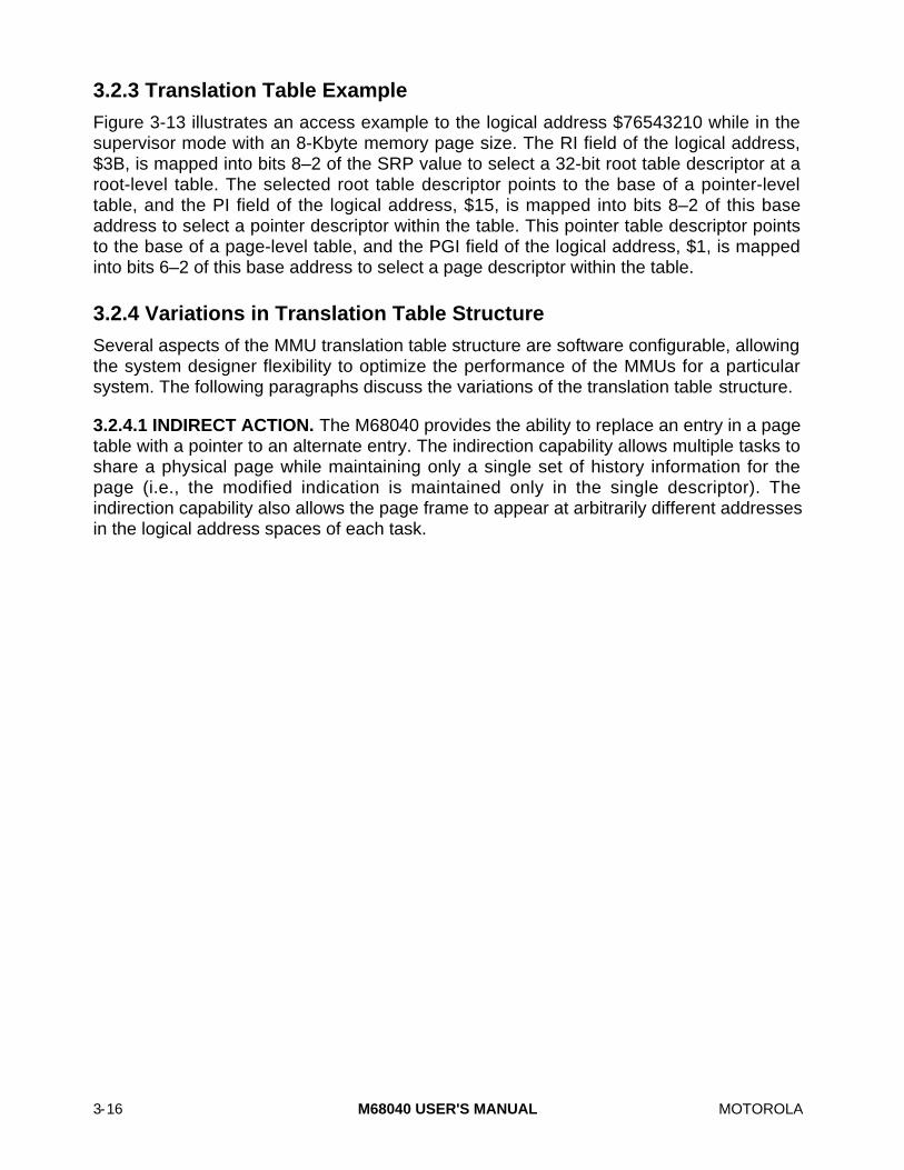
3-16 M68040 USER'S MANUAL MOTOROLA
3.2.3 Translation Table Example
Figure 3-13 illustrates an access example to the logical address $76543210 while in thesupervisor mode with an 8-Kbyte memory page size. The RI field of the logical address,$3B, is mapped into bits 8–2 of the SRP value to select a 32-bit root table descriptor at aroot-level table. The selected root table descriptor points to the base of a pointer-leveltable, and the PI field of the logical address, $15, is mapped into bits 8–2 of this baseaddress to select a pointer descriptor within the table. This pointer table descriptor pointsto the base of a page-level table, and the PGI field of the logical address, $1, is mappedinto bits 6–2 of this base address to select a page descriptor within the table.
3.2.4 Variations in Translation Table Structure
Several aspects of the MMU translation table structure are software configurable, allowingthe system designer flexibility to optimize the performance of the MMUs for a particularsystem. The following paragraphs discuss the variations of the translation table structure.
3.2.4.1 INDIRECT ACTION. The M68040 provides the ability to replace an entry in a pagetable with a pointer to an alternate entry. The indirection capability allows multiple tasks toshare a physical page while maintaining only a single set of history information for thepage (i.e., the modified indication is maintained only in the single descriptor). Theindirection capability also allows the page frame to appear at arbitrarily different addressesin the logical address spaces of each task.

MOTOROLA M68040 USER'S MANUAL 3-17
ROOT LEVEL TABLES
POINTER LEVEL TABLES
PAGE LEVEL TABLES
0 1 1 1 0 1 1 0 0 1 0 1 0 1 0 0 0 0 1 X X X X X X X X X X X X X
ROOT INDEX POINTER INDEX PAGE INDEX PAGE OFFSET
LOGICAL ADDRESS
$76543210 =
$3B $15 $01TABLE ENTRY # =
TABLE $3B TABLE $15SUPERVISOR MODE
TABLE $00
TABLE $7F TABLE $1F
TABLE $00 TABLE $00
$3B
$EC $54 $04ADDRESS OFFSET =
$00001800 $00003000 FRAME ADDRESS
SRP
$15 $01
Figure 3-13. Example Translation Table
Using the indirection capability, single entries or entire tables can be shared betweenmultiple tasks. Figure 3-14 illustrates two tasks sharing a page using indirect descriptors.
When the M68040 has completed a normal table search, it examines the PDT field of thelast entry fetched from the page tables. If the PDT field contains an indirect ($2) encoding,it indicates that the address contained in the highest order 30 bits of the descriptor is apointer to the page descriptor that is to be used to map the logical address. The processorthen fetches the page descriptor from this address and uses the physical address field ofthe page descriptor as the physical mapping for the logical address.
The page descriptor located at the address given by the indirect descriptor must not havea PDT field with an indirect encoding (it must be either a resident descriptor or invalid).Otherwise, the descriptor is treated as invalid, and the M68040 creates an ATC entry witha signaled error condition (R-bit in MMUSR is clear).
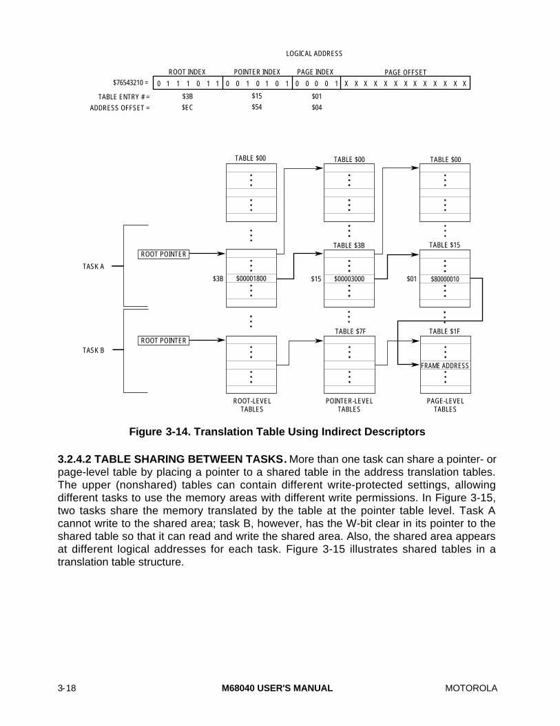
3-18 M68040 USER'S MANUAL MOTOROLA
ROOT-LEVEL TABLES
POINTER-LEVEL TABLES
PAGE-LEVEL TABLES
0 1 1 1 0 1 1 0 0 1 0 1 0 1 0 0 0 0 1 X X X X X X X X X X X X X
ROOT INDEX POINTER INDEX PAGE INDEX PAGE OFFSET
LOGICAL ADDRESS
$76543210 =
$3B $15 $01TABLE ENTRY # =
TABLE $3B TABLE $15
TABLE $00
TABLE $7F TABLE $1F
TABLE $00 TABLE $00
$3B
$EC $54 $04ADDRESS OFFSET =
$00001800 $00003000 $80000010$15 $01
ROOT POINTER
TASK A
TASK BROOT POINTER
FRAME ADDRESS
Figure 3-14. Translation Table Using Indirect Descriptors
3.2.4.2 TABLE SHARING BETWEEN TASKS. More than one task can share a pointer- orpage-level table by placing a pointer to a shared table in the address translation tables.The upper (nonshared) tables can contain different write-protected settings, allowingdifferent tasks to use the memory areas with different write permissions. In Figure 3-15,two tasks share the memory translated by the table at the pointer table level. Task Acannot write to the shared area; task B, however, has the W-bit clear in its pointer to theshared table so that it can read and write the shared area. Also, the shared area appearsat different logical addresses for each task. Figure 3-15 illustrates shared tables in atranslation table structure.

MOTOROLA M68040 USER'S MANUAL 3-19
ROOT-LEVEL TABLES
POINTER-LEVEL TABLES
PAGE-LEVEL TABLES
0 1 1 1 0 1 1 0 0 1 0 1 0 1 0 0 0 0 1 X X X X X X X X X X X X X
ROOT INDEX POINTER INDEX PAGE INDEX PAGE OFFSET
LOGICAL ADDRESS
$76543210 =
$3B $15 $01TABLE ENTRY # =
TABLE $3B TABLE $15
TABLE $00 TABLE $00 TABLE $00
$3B
$EC $54 $04ADDRESS OFFSET =
FRAME ADDRESS*
ROOT POINTER
$15 $01
TASK A
TASK BROOT POINTER
W-BIT CLEAR
* Page frame address shared by task A and B; write protected from task A.
W-BIT SET
$00003000
Figure 3-15. Translation Table Using Shared Tables
3.2.4.3 TABLE PAGING. The entire translation table for an active task need not beresident in main memory. In the same way that only the working set of pages must beallocated in main memory, only the tables that describe the resident set of pages need beavailable. Placing the invalid code ($0 or $1) in the UDT field of the table descriptor thatpoints to the absent table(s) implements this paging of tables. When a task attempts touse an address that an absent table would translate, the M68040 is unable to locate atranslation and takes access error exception when the execution unit retries the busaccess that caused the table search to be initiated.
The operating system determines that the invalid code in the descriptor corresponds tononresident tables. This determination can be facilitated by using he unused bits in thedescriptor to store status information concerning the invalid encoding. The M68040 doesnot interpret or modify an invalid descriptor’s fields except for the UDT field. This

3-20 M68040 USER'S MANUAL MOTOROLA
interpretation allows the operating system to store system-defined information in theremaining bits. Information typically stored includes the reason for the invalid encoding(tables paged out, region unallocated, etc.) and possibly the disk address for nonresidenttables. Figure 3-16 illustrates an address translation table in which only a single pagetable (table $15) is resident; all other page tables are not resident.
$15 $01
TABLE $3B
$3B
SUPERVISOR TABLE $00 TABLE $00
UDT = INVALID
UDT = INVALID
UDT = INVALID
UDT = INVALIDUDT = RESIDENT
POINTER-LEVEL TABLES
PAGE-LEVEL TABLES
TABLE $7F
TABLE $15
TABLE $00
TABLE $1F
UDT = INVALID
UDT = INVALID
UDT = INVALID
UDT = INVALID
UDT = RESIDENT
SRP
0 1 1 1 0 1 1 0 0 1 0 1 0 1 0 0 0 0 1 X X X X X X X X X X X X X
ROOT INDEX POINTER INDEX PAGE INDEX PAGE OFFSET
LOGICAL ADDRESS
$76543210 =
$3B $15 $01TABLE ENTRY # =$EC $54 $04ADDRESS OFFSET =
FRAME ADDRESS
NONRESIDENT(PAGED OR
UNALLOCATED)
ROOT-LEVEL TABLES
NONRESIDENT(PAGED OR
UNALLOCATED)
NONRESIDENT(PAGED OR
UNALLOCATED)
NONRESIDENT(PAGED OR
UNALLOCATED)
NONRESIDENT(PAGED OR
UNALLOCATED)
NONRESIDENT(PAGED OR
UNALLOCATED)
Figure 3-16. Translation Table with Nonresident Tables

MOTOROLA M68040 USER'S MANUAL 3-21
3.2.4.4 DYNAMICALLY ALLOCATED TABLES. Similar to paged tables, a completetranslation table need not exist for an active task. The operating system can dynamicallyallocate the translation table based on requests for access to particular areas.
As in demand paging, it is difficult, if not impossible, to predict the areas of memory that atask uses over any extended period. Instead of attempting to predict the requirements ofthe task, the operating system performs no action for a task until a demand is maderequesting access to a previously unused area or an area that is no longer resident inmemory. This technique can be used to efficiently create a translation table for a task.
For example, consider an operating system that is preparing the system to execute apreviously unexecuted task that has no translation table. Rather than guessing what thememory-usage requirements of the task are, the operating system creates a translationtable for the task that maps one page corresponding to the initial value of the programcounter (PC) for that task and one page corresponding to the initial stack pointer of thetask. All other branches of the translation table for this task remain unallocated until thetask requests access to the areas mapped by these branches. This technique allows theoperating system to construct a minimal translation table for each task, conservingphysical memory utilization and minimizing operating system overhead.
3.2.5 Table Search Accesses
The cache treats table search accesses that are not read-modify-write accesses ascachable/write-through but do not allocate in the cache for misses. Read-modify-writetable search accesses (required to update some descriptor U-bit and M-bit combinations)are treated as noncachable and force a matching cache line to be pushed and invalidated.Table search bus accesses are locked only for the specific portions of the table searchthat requires a read-modify-write access.
During a table search, the U-bit in each encountered descriptor is checked and set if notalready set. Similarly, when the table search is for a write access and the M-bit of thepage descriptor is clear, the processor sets the bit if the table search does not encounter aset W-bit or a supervisor violation. Repeating the descriptor access as part of a read-modify-write access updates specific combinations of the U and M bits, allowing theexternal arbiter to prevent the update operation from being interrupted.
The M68040 asserts the LOCK signal during certain portions of the table search to ensureproper maintenance of the U-bit and M-bit. The U-bit and M-bit are updated before theM68040 allows a page to be accessed or written. As descriptors are fetched, the U-bit andM-bit are monitored. Write cycles modify these bits when required. For a table descriptor,a write cycle that sets the U-bit occurs only if the U-bit was clear. Table 3-1 lists the pagedescriptor update operations for each combination of U-bit, M-bit, write-protected, andread or write access type.

3-22 M68040 USER'S MANUAL MOTOROLA
Table 3-1. Updating U-Bit and M-Bit for Page Descriptors
Previous Status Access Page Descriptor New Status
U-Bit M-Bit WP Bit Type Update Operation U-Bit M-Bit
0 0 Locked RMW Access to Set U 1 0
0 1 Locked RMW Access to Set U 1 1
1 0 X Read None 1 0
1 1 None 1 1
0 0 Write to Set U and M 1 1
0 1 Locked RMW Access to Set U 1 1
1 0 0 Write to Set M 1 1
1 1 Write None 1 1
0 0 Locked RMW Access to Set U 1 0
0 1 Locked RMW Access to Set U 1 1
1 0 1 None 1 0
1 1 None 1 1
NOTE: WP indicates the accumulated write-protect status.
An alternate address space access is a special case that is immediately used as aphysical address without translation. Because the M68040 implements a mergedinstruction and data space, the integer unit translates MOVES accesses to instructionaddress spaces (SFC/DFC = $6 or $2) into data references (SFC/DFC = $5 or $1). Thedata memory unit handles these translated accesses as normal data accesses. If theaccess fails due to an ATC fault or a physical bus error, the resulting access error stackframe contains the converted function code in the TM field for the faulted access.Invalidation of the instruction cache line containing the referenced location to maintaincache coherency must precede MOVES accesses that write the instruction addressspace. The SFC and DFC values and results are listed in Table 3-2.
Table 3-2. SFC and DFC Values
Results
SFC/DFC Value TT TM
000 10 000
001 00 001
010 00 001
011 10 011
100 10 100
101 00 101
110 00 101
111 10 111

MOTOROLA M68040 USER'S MANUAL 3-23
3.2.6 Address Translation Protection
The M68040 MMUs provide separate translation tables for supervisor and user addressspaces. The translation tables contain both mapping and protection information. Eachtable and page descriptor includes a write-protect (W) bit that can be set to provide writeprotection at any level. Page descriptors also contain a supervisor-only (S) bit that canlimit access to programs operating at the supervisor privilege level.
The protection mechanisms can be used individually or in any combination to protect:
• Supervisor address space from accesses by user programs.
• User address space from accesses by other user programs.
• Supervisor and user program spaces from write accesses (implicitly supported bydesignating all memory pages used for program storage as write protected).
• One or more pages of memory from write accesses.
3.2.6.1 SUPERVISOR AND USER TRANSLATION TABLES. One way of protectingsupervisor and user address spaces from unauthorized accesses is to use separatesupervisor and user translation tables. Separate trees protect supervisor programs anddata from accesses by user programs and user programs and data from access bysupervisor programs. Access is granted to the supervisor programs that can accesses anyarea of memory with MOVES. The translation table pointed to by the SRP is selected forall other supervisor mode accesses. This translation table can be common to all tasks.Figure 3-17 illustrates separate translation tables for supervisor accesses and for two usertasks that share the common supervisor space. Each user task has an translation tablewith unique mappings for the logical addresses in its user address space.
3.2.6.2 SUPERVISOR ONLY. A second mechanism protects supervisor programs anddata without requiring segmenting of the logical address space into supervisor and useraddress spaces. Page descriptors contain S-bits to protect areas of memory from accessby user programs. When a table search for a user access encounters an S-bit set in apage descriptor, the table search ends, and an ATC descriptor corresponding to thelogical address is created with the S-bit set. A subsequent retry of the user access resultsin an access error exception being taken. The S-bit can be used to protect one or morepages from user program access. Supervisor and user mode accesses can sharedescriptors by using indirect descriptors or by sharing tables. The entire user andsupervisor address spaces can be mapped together by loading the same root pointeraddress into both the SRP and URP registers.

3-24 M68040 USER'S MANUAL MOTOROLA
FOR TASK 'A'
URP FOR TASK 'A'USER A LEVEL TABLE
TRANSLATIONTABLE FORTASK 'A'
•
••
FOR TASK 'B'
URP FOR TASK 'B'USER A LEVEL TABLE
TRANSLATIONTABLE FORTASK 'B'
•
••
POINTER
COMMON SRPSUPERVISOR A LEVEL TABLE
TRANSLATIONTABLE FORALL SUPERVISORACCESSES
•
••
Figure 3-17. Translation Table Structure for Two Tasks
3.2.6.3 WRITE PROTECT. The M68040 provides write protection independent of otherprotection mechanisms. All table and page descriptors contain W-bits to protect areas ofmemory from write accesses of any kind, including supervisor writes. An ATC descriptorcorresponding to the logical address is created with the W-bit set after the table search iscompleted when a table search encounters a W-bit set in any table or page descriptor.The subsequent retry of the write access results in an access error exception being taken.The W-bit can be used to protect the entire area of memory defined by a branch of thetranslation table or protect only one or more pages from write accesses. Figure 3-18illustrates a memory map of the logical address space organized to use supervisor-onlyand write-protect bits for protection. Figure 3-19 illustrates an example translation table forthis technique.
SUPERVISOR AND USER SPACE
THIS AREA IS SUPERVISOR ONLY, READ-ONLY
THIS AREA IS SUPERVISOR ONLY, READ/WRITE
THIS AREA IS SUPERVISOR OR USER, READ-ONLY
THIS AREA IS SUPERVISOR OR USER, READ/WRITE
Figure 3-18. Logical Address Map with SharedSupervisor and User Address Spaces

MOTOROLA M68040 USER'S MANUAL 3-25
PRIVILEGE MODE
SRPURP
URP & SRP POINTTO SAME A LEVEL
TABLE
W =1
W = 1
W = 0
W = 0
S = 1,W = X
THIS PAGESUPERVISOR ONLY,
READ ONLY
W = 0 S = 1,W = 0
POINTER-LEVEL TABLE
PAGE-LEVEL TABLE
W = 0 S = 0,W = 0
THIS PAGESUPERVISOR ONLY,
READ/WRITE
THIS PAGESUPERVISOR/USER,
READ ONLY
THIS PAGESUPERVISOR/USER,
READ/WRITE
W = X S = 0,W = X
NOTE: X = Don’t care.
W = X
ROOT-LEVEL TABLE
Figure 3-19. Translation Table Using S-Bit and W-Bit To Set Protection
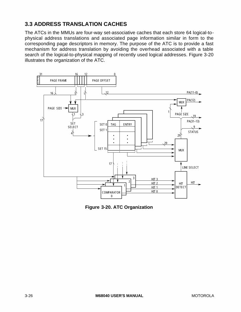
3-26 M68040 USER'S MANUAL MOTOROLA
3.3 ADDRESS TRANSLATION CACHES
The ATCs in the MMUs are four-way set-associative caches that each store 64 logical-to-physical address translations and associated page information similar in form to thecorresponding page descriptors in memory. The purpose of the ATC is to provide a fastmechanism for address translation by avoiding the overhead associated with a tablesearch of the logical-to-physical mapping of recently used logical addresses. Figure 3-20illustrates the organization of the ATC.
3
PAGE FRAME PAGE OFFSET
MUX
MUX
MUX
21
COMPARATOR 0
STATUS
PA(31–13)
PA(11–0)
PA(12)
PAGE SIZE
PAGE SIZE
116
3
1 12
1
17
29
19
9
1
4
17
0121631
HIT 3HIT 2HIT 1HIT 0
HITHIT DETECT
LINE SELECT
TAG ENTRY
29
F C
SET 0
SET 1
SET 15
TAG ENTRY
• • •
• • •
SET SELECT
2
Figure 3-20. ATC Organization

MOTOROLA M68040 USER'S MANUAL 3-27
Each ATC entry consists of a physical address, attribute information from a correspondingpage descriptor, and a tag that contains a logical address and status information. Figure3-21, which illustrates the entry and tag fields, is followed by field definitions listed inalphabetical order.
U1 U0 S CM M W R PHYSICAL ADDRESS*
ENTRY
V G FC2 LOGICAL ADDRESS*
TAG
* For 4-Kbyte page sizes this field uses address bits 31–12; for 8-Kbyte page sizes, bits 31–13.
Figure 3-21. ATC Entry and Tag Fields
CM—Cache ModeThis field selects the cache mode and accesses serialization as follows:
00 = Cachable, Write-through01 = Cachable, Copyback10 = Noncachable, Serialized11 = Noncachable
Section 4 Instruction and Data Caches provides detailed information on cachingmodes, and Section 7 Bus Operation provides information on serialization.
FC2—Function Code Bit 2 (Supervisor/User)This bit contains the function code corresponding to the logical address in this entry.FC2 is set for supervisor mode accesses and cleared for user mode accesses.
G—GlobalWhen set, this bit indicates the entry is global. Global entries are not invalidated by thePFLUSH instruction variants that specify nonglobal entries, even when all otherselection criteria are satisfied.
Logical AddressThis 13-bit field contains the most significant logical address bits for this entry. All 16bits of this field are used in the comparison of this entry to an incoming logical addresswhen the page size is 4 Kbytes. For 8-Kbytes pages, the least significant bit of this fieldis ignored.
M—ModifiedThe modified bit is set when a valid write access to the logical address corresponding tothe entry occurs. If the M-bit is clear and a write access to this logical address isattempted, the M68040 suspends the access, initiates a table search to set the M-bit inthe page descriptor, and writes over the old ATC entry with the current page descriptorinformation. The MMU then allows the original write access to be performed. This
3-28 M68040 USER'S MANUAL MOTOROLA
procedure ensures that the first write operation to a page sets the M-bit in both the ATCand the page descriptor in the translation tables, even when a previous read operationto the page had created an entry for that page in the ATC with the M-bit clear.
Physical AddressThe upper bits of the translated physical address are contained in this field.
R—ResidentThis bit is set if the table search successfully completes without encountering either anonresident page or a transfer error acknowledge during the search.
S—Supervisor ProtectedThis bit identifies a pointer table or a page as a supervisor-only table or page. Onlyprograms operating in the supervisor privilege mode are allowed to access the portionof the logical address space mapped by this descriptor when the S-bit is set. If the bit isclear, both supervisor and user accesses are allowed.
U0, U1—User Page AttributesThese user-defined bits are not interpreted by the M68040. U0 and U1 are echoed tothe UPA0 and UPA1 signals, respectively, if an external bus transfer results from theaccess.
V—ValidWhen set, this bit indicates the validity of the entry. This bit is set when the M68040loads an entry. A flush operation by a PFLUSH or PFLUSHA instruction that selects thisentry clears the bit.
W—Write ProtectedThis write-protect bit is set when a W-bit is set in any of the descriptors encounteredduring the table search for this entry. Setting a W-bit in a table descriptor write protectsall pages accessed with that descriptor. When the W-bit is set, a write access or a read-modify-write access to the logical address corresponding to this entry causes an accesserror exception to be taken immediately.
For each access to a memory unit, the MMU uses the four bits of the logical addresslocated just above the page offset (LA16–LA13 for 8K pages, LA15–LA12 for 4K pages) toindex into the ATC. The tags are compared with the remaining upper bits of the logicaladdress and FC2. If one of the tags matches and is valid, then the multiplexer choses thecorresponding entry to produce the physical address and status information. The ATCoutputs the corresponding physical address to the cache controller, which accesses thedata within the cache and/or requests an external bus cycle. Each ATC entry contains alogical address, a physical address, and status bits.
When the ATC does not contain the translation for a logical address, a miss occurs. TheMMU aborts the current access and searches the translation tables in memory for thecorrect translation. If the table search completes without any errors, the MMU stores the
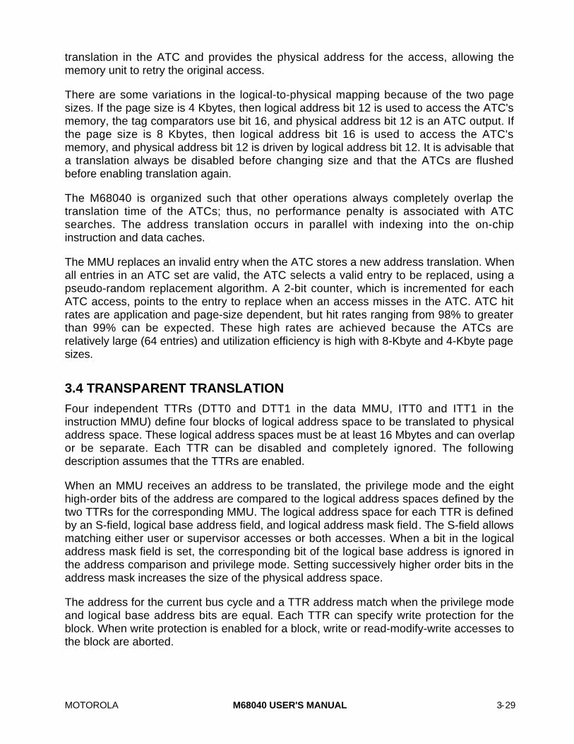
MOTOROLA M68040 USER'S MANUAL 3-29
translation in the ATC and provides the physical address for the access, allowing thememory unit to retry the original access.
There are some variations in the logical-to-physical mapping because of the two pagesizes. If the page size is 4 Kbytes, then logical address bit 12 is used to access the ATC'smemory, the tag comparators use bit 16, and physical address bit 12 is an ATC output. Ifthe page size is 8 Kbytes, then logical address bit 16 is used to access the ATC'smemory, and physical address bit 12 is driven by logical address bit 12. It is advisable thata translation always be disabled before changing size and that the ATCs are flushedbefore enabling translation again.
The M68040 is organized such that other operations always completely overlap thetranslation time of the ATCs; thus, no performance penalty is associated with ATCsearches. The address translation occurs in parallel with indexing into the on-chipinstruction and data caches.
The MMU replaces an invalid entry when the ATC stores a new address translation. Whenall entries in an ATC set are valid, the ATC selects a valid entry to be replaced, using apseudo-random replacement algorithm. A 2-bit counter, which is incremented for eachATC access, points to the entry to replace when an access misses in the ATC. ATC hitrates are application and page-size dependent, but hit rates ranging from 98% to greaterthan 99% can be expected. These high rates are achieved because the ATCs arerelatively large (64 entries) and utilization efficiency is high with 8-Kbyte and 4-Kbyte pagesizes.
3.4 TRANSPARENT TRANSLATION
Four independent TTRs (DTT0 and DTT1 in the data MMU, ITT0 and ITT1 in theinstruction MMU) define four blocks of logical address space to be translated to physicaladdress space. These logical address spaces must be at least 16 Mbytes and can overlapor be separate. Each TTR can be disabled and completely ignored. The followingdescription assumes that the TTRs are enabled.
When an MMU receives an address to be translated, the privilege mode and the eighthigh-order bits of the address are compared to the logical address spaces defined by thetwo TTRs for the corresponding MMU. The logical address space for each TTR is definedby an S-field, logical base address field, and logical address mask field. The S-field allowsmatching either user or supervisor accesses or both accesses. When a bit in the logicaladdress mask field is set, the corresponding bit of the logical base address is ignored inthe address comparison and privilege mode. Setting successively higher order bits in theaddress mask increases the size of the physical address space.
The address for the current bus cycle and a TTR address match when the privilege modeand logical base address bits are equal. Each TTR can specify write protection for theblock. When write protection is enabled for a block, write or read-modify-write accesses tothe block are aborted.

3-30 M68040 USER'S MANUAL MOTOROLA
By appropriately configuring a TTR, flexible transparent mappings can be specified (referto 3.1.3 Transparent Translation Registers for field identification). For instance, totransparently translate the user address space, the S-field is set to $0, and the logicaladdress mask is set to $FF in both an instruction and data TTR. To transparently translatesupervisor accesses of addresses $00000000–$0FFFFFFF with write protection, thelogical base address field is set to $0x, the logical address mask is set to $0F, the W-bit isset to one, and the S-field is set to $1. The inclusion of independent TTRs in both theinstruction and data MMUs provides an exception to the merged instruction and dataaddress space, allowing different translations for instruction and operand accesses. Also,since the instruction memory unit is only used for instruction prefetches, differentinstruction and data TTRs can cause PC relative operand fetches to be translateddifferently from instruction prefetches.
If either of the TTRs matched during an access to a memory unit (either instruction ordata), the access is transparently translated. If both registers match, the TT0 status bitsare used for the access. Transparent translation can also be implemented by thetranslation tables of the translation tables if the physical addresses of pages are set equalto their logical addresses.
3.5 ADDRESS TRANSLATION SUMMARY
The instruction and data MMUs process translations by first comparing the logical addressand privilege mode with the parameters of the TTRs. If there is a match, the MMU usesthe logical address as a physical address for the access. If there is no match, the MMUcompares the logical address and privilege mode with the tag portions of the entries in theATC and uses the corresponding physical address for the access when a match occurs.When neither a TTR nor a valid ATC entry matches, the MMU initiates a table searchoperation to obtain the corresponding physical address from the translation table. When atable search is required, the processor suspends instruction execution activity and, at theend of a successful table search, stores the address mapping in the appropriate ATC andretries the access. The MMU creates a valid ATC entry for the logical address, and theaccess is retried. If an access hits in the ATC but an access error or invalid pagedescriptor was detected during the table search that created the ATC entry, the access isaborted, and a bus error exception is taken.
If a write or read-modify-write access results in an ATC hit but the page is write protected,the access is aborted, and an access error exception is taken. If the page is not writeprotected and the modified bit of the ATC entry is clear, a table search proceeds to set themodified bit in both the page descriptor in memory and in the ATC; the access is retried.The ATC provides the address translation for the access if the modified bit of the ATCentry is set for a write or read-modify-write access to an unprotected page, if the residentbit is set (indicating the table search for the entry completed successfully), and if none ofthe TTRs (instruction or data, as appropriate) match.
An ATC access error is not reported immediately, if the last 16 bits of a page is either anA-line, illegal, CHK, or unimplemented instruction and the next page is non-resident.Instead, the M68040 attempts to prefetch the next instruction on the missing page, thenthe ATC access error exception is reported. The stacked PC points to the exceptional

MOTOROLA M68040 USER'S MANUAL 3-31
instruction, and the stacked FA points to the first longword in the missing page. When anATC access error occurs while prefetching the next instruction on the non-existant pageafter a change of flow instruction, the exception should be cleared by execution of the newinstruction flow. Either avoid this scenario, or have a dummy resident page following theexceptional instruction.
Figure 3-22 illustrates a general flowchart for address translation. The top branch of theflowchart applies to transparent translation. The bottom three branches apply to ATCtranslation.
3.6 MMU EFFECT ON RSTI AND MDIS
The following paragraphs describe MMU effects on the RSTI and MDIS pins.
3.6.1 Effect of RSTI on the MMUs
When the M68040 is reset by the assertion of the reset input signal, the E-bits of the TCRand TTRs are cleared, disabling address translation. This reset causes logical addressesto be passed through as physical addresses, allowing an operating system to set up thetranslation tables and MMU registers as required. After the translation tables and registersare initialized, the E-bit of the TCR can be set, enabling paged address translation. Whileaddress translation is disabled, the attribute bits for an access that an ATC entry or a TTRnormally supplies are zero, selecting write-through cachable mode, no write protection,and user page attribute bits cleared. RSTI does not affect the P-bit of the TCR.
A reset of the processor does not invalidate any entries in the ATCs or alter the page size.A PFLUSH instruction must be executed to flush all existing valid entries from the ATCsafter a reset operation and before translation is enabled. PFLUSH can be executed even ifthe E-bit is cleared.
3.6.2 Effect of MDIS on Address Translation
The assertion of MDIS prevents the MMUs from performing ATC searches and theexecution unit from performing table searches. With address translation disabled, logicaladdresses are used as physical addresses. MDIS disables the MMUs on the next internalaccess boundary when asserted and enables the MMUs on the next boundary after thesignal is negated. The assertion of this signal does not affect the operation of thetransparent translation registers or execution of the PFLUSH or PTEST instructions.
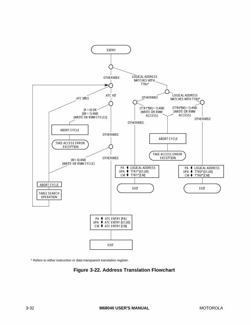
3-32 M68040 USER'S MANUAL MOTOROLA
ENTRY
EXIT
OTHERWISE
TAKE ACCESS ERROR EXCEPTION
ABORT CYCLE
ATC HIT
OTHERWISE
ABORT CYCLE
TABLE SEARCH OPERATION
TAKE ACCESS ERROR EXCEPTION
EXIT
OTHERWISE
PA ATC ENTRY [PA] UPA ATC ENTRY [U1,U0] CM ATC ENTRY [CM]
PA LOGICAL ADDRESS UPA TTR1* [U1,U0] CM TTR1* [CM]
EXIT
PA LOGICAL ADDRESS UPA TTR0* [U1,U0] CM TTR0* [CM]
ABORT CYCLE
(TTR1*[W] = 1) AND (WRITE OR RMW
ACCESS)
(TTR0*[W] = 1) AND (WRITE OR RMW
ACCESS)
LOGICAL ADDRESS MATCHES WITH TTR0*OTHERWISEATC MISS
(R = 0) OR [(W = 1) AND
(WRITE OR RMW CYCLE)]
LOGICAL ADDRESS MATCHES WITH
TTRx*
OTHERWISE
OTHERWISE(M = 0) AND (WRITE OR RMW CYCLE)
* Refers to either instruction or data transparent translation register.
Figure 3-22. Address Translation Flowchart

MOTOROLA M68040 USER'S MANUAL 3-33
3.7 MMU INSTRUCTIONS
The M68040 instruction set includes three privileged instructions that perform MMUoperations. The following paragraphs briefly describe each of these instructions. Fordetailed descriptions of these instructions, refer to M68000PR/AD, M68000 FamilyProgrammer's Reference Manual.
3.7.1 MOVEC
The MOVEC instruction transfers data between an integer data register, or memorylocation, and any of the M68040 control and status registers. The operating system usesthe MOVEC instruction to control and monitor MMU operation by manipulating andreading the eight MMU registers.
3.7.2 PFLUSH
The PFLUSH instruction flushes or invalidates address translation descriptors in theATCs. PFLUSHA, a version of the PFLUSH instruction, flushes all entries. The PFLUSHinstruction flushes a user or supervisor entry with a specified logical address. ThePFLUSHAN and PFLUSHN instruction variants qualify entry selection further by flushingonly entries that are nonglobal, indicated by a cleared G-bit in the entry.
3.7.3 PTEST
The PTEST instruction performs a table search operation for a specified function code andlogical address and sets the appropriate bit fields in the MMUSR to indicate conditionsencountered during the search. PTEST automatically flushes the corresponding entry fromthe cache before searching the tables and loads the latest information from the translationtables into the ATC. The exception routines of the operating system can use thisinstruction to identify MMU faults.
PTEST is primarily used in access error exception handlers. For example, if a bus errorhas occurred, the handler can execute an instruction sequence such as the followingsequence:
MOVE.B (A7,offset1),D0 Copy transfer modifier field from stack frameMOVEC D0,DFC into DFC registerMOVEA.L (A7,offset2),A0 Copy fault address from stack frame into address registerPTESTW (A0) Test address in A0 with function code in DFC registers
The transfer modifier field copied into the destination function code (DFC) registerindicates whether the faulted access was a supervisor or user mode access and whetherit was an instruction prefetch or data access. The PTEST instruction uses the DFC valueto determine which translation table (supervisor or user) to search and which ATC (data orinstruction) to create the entry in. After executing this code sequence, the handler canexamine the MMUSR for the source of the fault.
The M68040 MMU instructions use opcodes that are different from those for thecorresponding instructions in the MC68030 and MC68851. All MMU opcodes for the

3-34 M68040 USER'S MANUAL MOTOROLA
MC68030 and MC68851 cause F-line unimplemented instruction exceptions if executed ineither supervisor or user mode by the M68040.
3.7.4 Register Programming Considerations
If the entries in the ATCs are no longer valid when a reset operation occurs (as is normallyexpected), an explicit flush operation must be specified by the system software. Theassertion of RSTI disables translation by clearing the E-bits of the TCR, DTTRx, andITTRx, but it does not flush the ATCs. Reading or writing any of the MMU registers (URP,SRP, TCR, MMUSR, DTTR0, DTTR1, ITTR0, ITTR1) does not flush the ATCs. Since awrite to these registers can cause some or all the address translations to change, the writeshould be followed by a PFLUSH operation to flush the ATCs if necessary.
The status bits in the MMUSR indicate conditions to which the operating system shouldrespond. In a typical access error exception handler, the flowchart illustrated in Figure3-23 can be used to determine the cause of an MMU fault. The PTEST instruction setsthe bits in the MMUSR appropriately, and the program can branch to the appropriate codesegment for the condition.
MOTOROLA M68040 USER'S MANUAL 3-35
BRANCH TO "SUPERVISOR VOILATION" CODE
BRANCH TO "WRITE VIOLATION" CODE
BRANCH TO "WRITE VIOLATION" CODE
PTEST (An)
BRANCH TO "PAGE FAULT" OR "INVALID DESCRIPTOR" CODE
BRANCH TO "BUS ERROR DURING TABLE SEARCH" CODE
NOT MMU
R = 0
B = 0B = 1R = 1
T = 1T = 0
OTHERWISE MATCH TTR0*
OTHERWISE OTHERWISE
MATCH TTR1*
OTHERWISE
TTR1*[W] = 1 AND (WRITE OR RMW ACCESS INDICATED IN
STACK FRAME)
TTR0*[W] = 1 AND (WRITE OR RMW ACCESS INDICATED IN
STACK FRAME)
WRITE OR RMW ACCESS INDICATED IN STACK
FRAME
W = 1
OTHERWISE
W = 0
OTHERWISE
S = 1 AND (USER ACCESS INDICATED IN STACK FRAME)
NOT MMU
* Refers to either instruction or data transparent translation register.
Figure 3-23. MMU Status Interpretation

3-36 M68040 USER'S MANUAL MOTOROLA

MOTOROLA M68040 USER’S MANUAL 4-1
SECTION 4INSTRUCTION AND DATA CACHES
NOTE
Ignore all references to the memory management unit (MMU)when reading for the MC68EC040 and MC68EC040V. Thefunctionality of the MC68040 transparent translation registershas been changed in the MC68EC040 and MC68EC040V tothe access control registers. Refer to Appendix BMC68EC040 for details.
The M68040 contains two independent, 4-Kbyte, on-chip caches located in the physicaladdress space. Accessing instruction words and data simultaneously through separatecaches increases instruction throughput. The M68040 caches improve systemperformance by providing cached data to the on-chip execution unit with very low latency.Systems with an alternate bus master receive increased bus availability.
Figure 4-1 illustrates the instruction and data caches contained in the instruction and datamemory units. The appropriate memory unit independently services instruction prefetchand data requests from the integer unit (IU). The memory units translate the logicaladdress in parallel with indexing into the cache. If the translated address matches one ofthe cache entries, the access hits in the cache. For a read operation, the memory unitsupplies the data to the IU, and for a write operation, the memory unit updates the cache.If the access does not match one of the cache entries (misses in the cache) or a writeaccess must be written through to memory, the memory unit sends an external busrequest to the bus controller. The bus controller then reads or writes the required data.
Cache coherency in the M68040 is optimized for multimaster applications in which theM68040 is the caching master sharing memory with one or more noncaching masters(such as DMA controllers). The M68040 implements a bus snooper that maintains cachecoherency by monitoring an alternate bus master’s access and performing cachemaintenance operations as requested by the alternate bus master. Matching cache entriescan be invalidated during the alternate bus master’s access to memory, or memory can beinhibited to allow the M68040 to respond to the access as a slave. For an external writeoperation, the processor can intervene in the access and update its internal caches (sinkdata). For an external read operation, the processor supplies cached data to the alternatebus muster (source data). This prevents the M68040 caches from accumulating old orinvalid copies of data (stale data). Alternate bus masters are allowed access to locallymodified data within the caches that is no longer consistent with external memory (dirtydata). Allowing memory pages to be specified as write-through instead of copyback alsosupports cache coherency. When a processor writes to write-through pages, external

4-2 M68040 USER'S MANUAL MOTOROLA
memory is always updated through an external bus access after updating the cache,keeping memory and cached data consistent.
INSTRUCTION FETCH
DECODE
EA CALCULATE
EXECUTE
WRITEBACK
EA FETCH
INTEGER UNIT
CONVERT
EXECUTE
WRITE- BACK
INSTRUCTION ATC
INSTRUCTION MMU/CACHE/SNOOP
CONTROLLER
BUS CONTROL SIGNALS
DATA BUS
ADDRESS BUS
DATA ATC
DATA MMU/CACHE/SNOOP
CONTROLLER
OPERAND DATA BUS
INSTRUCTION DATA BUS
INSTRUCTION CACHE
DATA CACHE
FLOATING- POINT UNIT
DATA MEMORY UNIT
INSTRUCTION MEMORY UNIT B U S
C O N T R O L L E R
INSTRUCTION ADDRESS
DATA ADDRESS
Figure 4-1. Overview of Internal Caches
4.1 CACHE OPERATION
Both four-way set-associative caches have 64 sets of four 16-byte lines. There are twoformats that define each cache line, an instruction cache line format and a data cache lineformat. Each format contains an address tag consisting of the upper 22 bits of the physicaladdress, status information, and four long words (128 bits) of data. The status informationfor the instruction cache line address tag consists of a single valid bit for the entire line.The status information for the data cache line address tag contains a valid bit and fouradditional bits to indicate dirty status for each long word in the line. Note that only the datacache supports dirty cache lines. Figure 4-2 illustrates the instruction cache line format (a)and the data cache line format (b).

MOTOROLA M68040 USER’S MANUAL 4-3
TAG V LW3 LW2 LW1 LW0
(a) Instruction Cache Line
TAG V LW3 D3 LW2 D2 LW1 D1 LW0 D0
TAG — 22-Bit Physical Address TagV — Line VALID Bit
LW — Long Word n (32-Bit) Data EntryDn — DIRTY Bit for Long Word n
(b) Data Cache Line
Figure 4-2. Cache Line Formats
The cache stores an entire line, providing validity on a line-by-line basis. Only burst modeaccesses that successfully read four long words can be cached. Memory devices unableto support bursting can respond to a cache line read or write access by asserting thetransfer burst inhibit (TBI) signal, forcing the processor to complete the access as asequence of three long-word accesses. The cache recognizes burst accesses as if theaccess were never inhibited, detecting no difference.
A cache line is always in one of three states: invalid, valid, or dirty. For invalid lines, the V-bit is clear, causing the cache line to be ignored during lookups. Valid lines have their V-bitset and D-bits cleared, indicating all four long words in the line contain valid dataconsistent with memory. Dirty cache lines have the V-bit and one or more D-bits set,indicating that the line has valid long-word entries that have not been written to memory(long words whose D-bit is set). A cache line changes from valid to invalid if the executionof the CINV or CPUSH instruction explicitly invalidates the cache line; if a snooped writeaccess hits the cache line and the line is not dirty; or if the SCx signals for a snooped readaccess invalidates the line. Both caches should be explicitly cleared after a hardware resetof the processor since reset does not invalidate the cache lines.
Figure 4-3 illustrates the general flow of a caching operation. The corresponding memoryunit translates the logical address of each access to a physical address allowing the IU toaccess the data in the cache. To minimize latency of the requested data, the loweruntranslated bits of the logical address map directly to the physical address bits and areused to access a set of cache lines in parallel with the translation. Physical address bits9–4 are used to index into the cache and select one of the 64 sets of four cache lines. Thefour tags from the selected cache set are compared with the translated physical addressbits 31–12 and bits 11 and 10 of the untranslated page offset. If any one of the four tagsmatches and the tag status is either valid or dirty, then the cache has a hit. During readaccesses, a half-line (two long words) is accessed at a time, requiring two cache accessesfor reads that are greater than a half-line or two long words. Write accesses within a cacheline require a single cache access. If a misaligned access crosses two pages, then thepartial access to the first page always happens twice, even if the pages are serialized.Consequently, if the accesses span page boundaries, misaligned accesses to peripheralsare not possible unless the peripheral can tolerate double reads or writes.

4-4 M68040 USER'S MANUAL MOTOROLA
S PAGE FRAME PAGE OFFSET
31 12 0
ADDRESS TRANSLATION
CACHE
PA11–PA10
0COMPARATOR
1
3
2HIT 3
HIT 2
HIT 1
HIT 0
HIT
TAG STATUS
TAG STATUS
SET 0
SET 1
SET 63
LINE 0
LINE 1
LINE 2
LINE 3
D0 D1 D2 D3
D0 D1 D2 D3
MUX
LOGICAL OR
LINE SELECT
DATA OR INSTRUCTION
PHYSICAL SET SELECT
PA9–PA4
SUPERVISOR BIT
LA31–LA12
LOGICAL ADDRESS
PA31–PA12
TRANSLATED PHYSICAL ADDRESS PA31–PA10
Figure 4-3. Caching Operation
Both caches contain circuitry to automatically determine which cache line in a set to usefor a new line. The cache controller locates the first invalid line and uses it; if no invalidlines exist, then a pseudo-random replacement algorithm is used to select a valid line,replacing it with the new line. Each cache contains a 2-bit counter, which is incrementedfor each access to the cache. The instruction cache counter is incremented for each half-line accessed in the instruction cache. The data cache counter is incremented for eachhalf-line accessed during reads, for each full line accessed during writes in copybackmode, and for each bus transfer resulting from a write in write-through mode. When amiss occurs and all four lines in the set are valid, the line pointed to by the current countervalue is replaced, after which the counter is incremented.

MOTOROLA M68040 USER’S MANUAL 4-5
4.2 CACHE MANAGEMENT
Using the MOVEC instruction, the caches are individually enabled to access the 32-bitcache control register (CACR) illustrated in Figure 4-4. The CACR contains two enablebits that allow the instruction and data caches to be independently enabled or disabled.Setting one of these bits enables the associated cache without affecting the state of anylines within the cache. A hardware reset clears the CACR, disabling both caches;however, reset does not affect the tags, state information, and data within the caches. TheCINV instruction must clear the caches before enabling them. It is not recommended thatpage descriptors be cached. Specifically, the M68040 does not support the caching ofpage descriptors in copyback mode with the bit pattern U = 0, M = 1, and R = 1 in a pagedescriptor. The M68040 table search algorithm will never leave this bit pattern for a pagedescriptor.
31 30 16 15 14 0
DE UNDEFINED IE UNDEFINED
DE = Enable Data CacheIE = Enable Instruction Cache
Figure 4-4. Cache Control Register
System hardware can assert the cache disable (CDIS) signal to dynamically disable bothcaches, regardless of the state of the enable bits in the CACR. The caches are disabledimmediately after the current access completes. If CDIS is asserted during the access forthe first half of a misaligned operand spanning two cache lines, the data cache is disabledfor the second half of the operand. Accesses by the execution units bypass the cacheswhile they are disabled and do not affect their contents (with the exception of CINV andCPUSH instructions). Disabling the caches with CDIS does not affect snoop operations.CDIS is intended primarily for use by in-circuit emulators to allow swapping between thetags and emulator memories.
Even if the instruction cache is disabled, the M68040 can cache instructions because ofan internal cache line register. This happens for instruction loops that are completelyresident within the first six bytes of a half-line. Thus, the cache line holding register canoperate as a small cache. If a loop fits anywhere within the first three words of a half-line,then it becomes cached.
The CINV and CPUSH instructions support cache management in the supervisor mode.CINV allows selective invalidation of cache entries. CPUSH performs two operations: 1)any selected data cache lines containing dirty data are pushed to memory; 2) all selectedcache lines are invalidated. This operation can be used to update a page in memorybefore swapping it out with snooping disabled or to push dirty data when changing a pagecaching mode to write-through. Because of the size of the caches, pushing pages or anentire cache incurs a significant time penalty. However, these instructions areinterruptable to avoid large interrupt latencies. The state of the CDIS signal or the cacheenable bits in the CACR does not affect the operation of CINV and CPUSH. Bothinstructions allow operation on a single cache line, all cache lines in a specific page, or an
4-6 M68040 USER'S MANUAL MOTOROLA
entire cache, and can select one or both caches for the operation. For line and pageoperations, a physical address in an address register specifies the memory address.
4.3 CACHING MODES
Every IU access to the cache has an associated caching mode that determines how thecache handles the access. An access can be cachable in either the write-through orcopyback modes, or it can be cache inhibited in nonserialized or serialized modes. TheCM field corresponding to the logical address of the access normally specifies, on a page-by-page basis, one of these caching modes. The default memory access caching mode isnonserialized. When the cache is enabled and memory management is disabled, thedefault caching mode is write-through. The transparent translation registers and MMUsallow the defaults to be overridden. In addition, some instructions and IU operationsperform data accesses that have an implicit caching mode associated with them. Thefollowing paragraphs discuss the different caching accesses and their related cachemodes.
4.3.1 Cachable Accesses
If a page descriptor’s CM field indicates write-through or copyback, then the access iscachable. A read access to a write-through or copyback page is read from the cache ifmatching data is found. Otherwise, the data is read from memory and used to update thecache. Since instruction cache accesses are always reads, the selection of write-throughor copyback modes do not affected them. The following paragraphs describe the write-through and copyback modes in detail.
4.3.1.1 WRITE-THROUGH MODE. Accesses to pages specified as write-through arealways written to the external address, although the cycle can be buffered, keepingmemory and cache data consistent. Writes in write-through mode are handled with a no-write-allocate policy—i.e., writes that miss in a data cache are written to memory but donot cause the corresponding line in memory to be loaded into the cache. Write accessesalways write through to memory and update matching cache lines. Specifying write-through mode for the shared pages maintains cache coherency for shared memory areasin a multiprocessing environment. The cache supplies data to instruction or data readaccesses that hit in the appropriate cache; misses cause a new cache line to be loadedinto the cache, replacing a valid cache line if there are no invalid lines.
4.3.1.2 COPYBACK MODE. Copyback pages are typically used for local data structuresor stacks to minimize external bus usage and reduce write access latency. Write accessesto pages specified as copyback that hit in the data cache update the cache line and setthe corresponding D-bits without an external bus access. The dirty cached data is onlywritten to memory if 1) the line is replaced due to a miss, 2) a cache inhibited accessmatches the line, or 3) the CPUSH instruction explicitly pushes the line. If a write accessmisses in the cache, the memory unit reads the needed cache line from memory andupdates the cache. When a miss causes a dirty cache line to be selected for replacement,the memory unit places the line in an internal copyback buffer. The replacement line isread into the cache, and writing the dirty cache line back to memory updates memory.

MOTOROLA M68040 USER’S MANUAL 4-7
4.3.2 Cache-Inhibited Accesses
Address space regions containing targets such as I/O devices and shared data structuresin multiprocessing systems can be designated cache inhibited. If a page descriptor’s CMfield indicates nonserialized or serialized, then the access is cache inhibited. The cachingoperation is identical for both cache-inhibited modes. If the CM field of a matching addressindicates either nonserialized or serialized modes, the cache controller bypasses thecache and performs an external bus transfer. The data associated with the access is notcached internally, and the cache inhibited out (CIOUT) signal is asserted during the bustransfer to indicate to external memory that the access should not be cached. If the datacache line is already resident in an internal cache, then the data cache line is pushed fromthe cache if it is dirty or the data cache line is invalidated if it is valid.
If the CM field indicates serialized, then the sequence of read and write accesses to thepage is guaranteed to match the sequence of the instruction order. Without serialization,the IU pipeline allows read accesses to occur before completion of a write-back for aprevious instruction. Serialization forces operand read accesses for an instruction to occuronly once by preventing the instruction from being interrupted after the operand fetchstage. Otherwise, the instruction is aborted, and the operand is accessed when theinstruction is restarted. These guarantees apply only when the CM field indicates theserialized mode and the accesses are aligned. Regardless of the selected cache mode,locked accesses are implicitly serialized. The TAS, CAS, and CAS2 instructions uselocked accesses for operands in memory and for updating translation table entries duringtable search operations.
4.3.3 Special Accesses
Several other processor operations result in accesses that have special cachingcharacteristics besides those with an implied cache-inhibited access in the serializedmode. Exception stack accesses, exception vector fetches, and table searches that missin the cache do not allocate cache lines in the data cache, preventing replacement of acache line. Cache hits by these accesses are handled in the normal manner according tothe caching mode specified for the accessed address.
Accesses by the MOVE16 instruction also do not allocate cache lines in the data cache foreither read or write misses. Read hits on either valid or dirty cache lines are read from thecache. Write hits invalidate a matching line and perform an external access. Interactingwith the cache in this manner prevents a large block move or block initializationimplemented with a MOVE16 from being cached, since the data may not be neededimmediately.
If the data cache is re-enabled after a locked access has hit and the data cache wasdisabled, the next non-locked access that results in a data cache miss will not be cached.
4.4 CACHE PROTOCOL
The cache protocol for processor and snooped accesses is described in the followingparagraphs. In all cases, an external bus transfer will cause a cache line state to change

4-8 M68040 USER'S MANUAL MOTOROLA
only if the bus transfer is marked as snoopable on the bus. The protocols described in thefollowing paragraphs assume that the data is cachable (i.e., write-through and copyback).
4.4.1 Read Miss
A processor read that misses in the cache causes the cache controller to request a bustransaction that reads the needed line from memory and supplies the required data to theIU. The line is placed in the cache in the valid state. Snooped external reads that miss inthe cache have no affect on the cache.
4.4.2 Write Miss
The cache controller handles processor writes that miss in the cache differently for write-through and copyback pages. Write misses to copyback pages cause the processor toperform a bus transaction that writes the needed cache line into its cache from memory inthe same manner as for a read miss. The new cache line is then updated with the writedata, and the D-bits are set for each long word that has been modified, leaving the cacheline in the dirty state. Write misses to write-through pages write directly to memory withoutloading the corresponding cache line in the cache. Snooped external writes that miss inthe cache have no affect on the cache.
4.4.3 Read Hit
The cache controller handles processor reads that hit in the cache differently for write-through and copyback pages. No bus transaction is performed, and the state of the cacheline does not change. Physical address bit 3 selects either the upper or lower half-linecontaining the required operand. This half-line is driven onto the internal bus. If therequired data is allocated entirely within the half-line, only one access into the cache isrequired. Because the organization of the cache does not allow selection of more than onehalf-line at a time, misalignment across a half-line boundary requires two accesses intothe cache.
A snooped external read that hits in the cache is ignored if the cache line is valid. If thesnooped access hits a dirty line, memory is inhibited from responding, and the data issourced from the cache directly to the alternate bus master. A snooped read hit does notchange the state of the cache line unless the snooped access also indicates mark invalid,which causes the line to be invalidated after the access, even if it is dirty. Alternate busmasters should indicate mark invalid only for line reads to ensure the entire line istransferred before invalidating.
4.4.4 Write Hit
The cache controller handles processor writes that hit in the cache differently for write-through and copyback pages. For write-through accesses, a processor write hit causesthe cache controller to update the affected long-word entries in the cache line and torequest an external memory write transfer to update memory. The cache line state doesnot change. A write-through access to a line containing dirty data constitutes a systemprogramming error even if the D-bits for the line are unchanged. This situation can be

MOTOROLA M68040 USER’S MANUAL 4-9
avoided by pushing cache lines when a page descriptor is changed and ensuring thatalternate bus masters indicate the appropriate snoop operation for writes to correspondingpages (i.e., mark invalid for write-through pages and sink data for copyback pages). If theaccess is copyback, the cache controller updates the cache line and sets the D-bit for ofthe appropriate long words in the cache line. An external write is not performed, and thecache line state changes to, or remains in, the dirty state.
An alternate bus master can drive the SCx signals for a write access with an encoding thatindicates to the M68040 that it should sink the data, inhibit memory, and respond as aslave if the access hits in the cache. The cache operation depends on the access size andcurrent line state. A snooped line write that hits a valid line always causes thecorresponding cache line to be invalidated. For snooped writes of byte, word, or long-wordsize that hit a dirty line, the processor inhibits memory and responds to the alternate busmaster as a slave, sinking the data. Data received from the alternate bus master is writtento the appropriate long word in the cache line, and the D-bit is set for that entry. The cachecontroller invalidates a cache line if the snoop control pins have indicated that a matchingcache line is marked invalid for a snoop write.
4.5 CACHE COHERENCY
The M68040 provides several different mechanisms to assist in maintaining cachecoherency in multimaster systems. Both write-through and copyback memory updatetechniques are supported to maintain coherency between the data cache and memory.
Alternate bus master accesses can reference data that the M68040 caches, causingcoherency problems if the accesses are not handled properly. The M68040 snoops thebus during alternate bus master transfers. If a write access hits in the cache, the M68040can update its internal caches, or if a read access hits, it can intervene in the access tosupply dirty data. Caches can be snooped even if they are disabled. The alternate busmaster controls snooping through the snoop control signals, indicating which access canbe snooped and the required operation for snoop hits. Table 4-1 lists the requested snoopoperation for each encoding of the snoop control signals. Since the processor and the bussnooper must both access the caches, the snoop controller has priority over the processorfor snoopable accesses to maintain cache coherency.
Table 4-1. Snoop Control Encoding
Requested Snoop Operation
SC1 SC0 Alternate Bus Master Read Access Alternate Bus Master Write Access
0 0 Inhibit Snooping Inhibit Snooping
0 1 Supply Dirty Data and Leave Dirty Data Sink Byte/Word/Long/Long Word
1 0 Supply Dirty Data and Mark Line Invalid Invalidate Line
1 1 Reserved (Snoop Inhibited) Reserved (Snoop Inhibited)
The snooping protocol and caching mechanism supported by the M68040 are optimized tosupport multimaster systems with the M68040 as the single caching master. In systems

4-10 M68040 USER'S MANUAL MOTOROLA
implementing multiple MC68040s as bus masters, shared data should be stored in write-through pages. This procedure allows each processor to cache shared data for readaccess while forcing a processor write to shared data to appear as an external write tomemory, which the other processors can snoop.
If shared data is stored in copyback pages, only one processor at a time can cache thedata since writes to copyback pages do not access the external bus. If a processoraccesses shared data cached by another processor, the slave can source the data to themaster without invalidating its own copy only if the transfer to the master is cacheinhibited. For the master processor to cache the data, it must force invalidation of theslave processor’s copy of the data (by specifying mark invalid for the snoop operation),and the memory controller must monitor the data transfer between the processors andupdate memory with the transferred data. The memory update is required since themaster processor is unaware of the sourced data (valid data from memory or dirty datafrom a snooping processor) and initially creates a valid cache line, losing dirty status if asnooping processor supplies the data.
Coherency between the instruction cache and the data cache must be maintained insoftware since the instruction cache does not monitor data accesses. Processor writesthat modify code segments (i.e., resulting from self-modifying code or from code executedto load a new page from disk) access memory through the data memory unit. Because theinstruction cache does not monitor these data accesses, stale data occurs in theinstruction cache if the corresponding data in memory is modified. Invalidating instructioncache lines before writing to the corresponding memory lines can prevent this coherencyproblem, but only if the data cache line is in write-through mode and the page is markedserialized. A cache coherency problem could arise if the data cache line is configured ascopyback and no serialization is done.
To fully support self-modifying code in any situation, it is imperative that a CPUSHAinstruction be executed before the execution of the first self-modified instruction. TheCPUSHA instruction has the effect of ensuring that there is no stale data in memory, thepipeline is flushed, and instruction prefetches are repeated and taken from externalmemory.
Another potential coherency problem exists due to the relationship between the cachestate information and the translation table descriptors. Because each cache line reflectspage state information, a page should be flushed from the cache before any of the pageattributes are changed. The presence of a valid or dirty cache line implicitly indicates thataccesses to the page containing the line are cachable. The presence of a dirty cache lineimplies that the page is not write protected and that writes to the page are in copybackmode. A system programming error occurs when page attributes are changed withoutflushing the corresponding page from the cache, resulting in cache line states inconsistentwith their page definitions. Even with these inconsistencies, the cache is defined andpredictable.
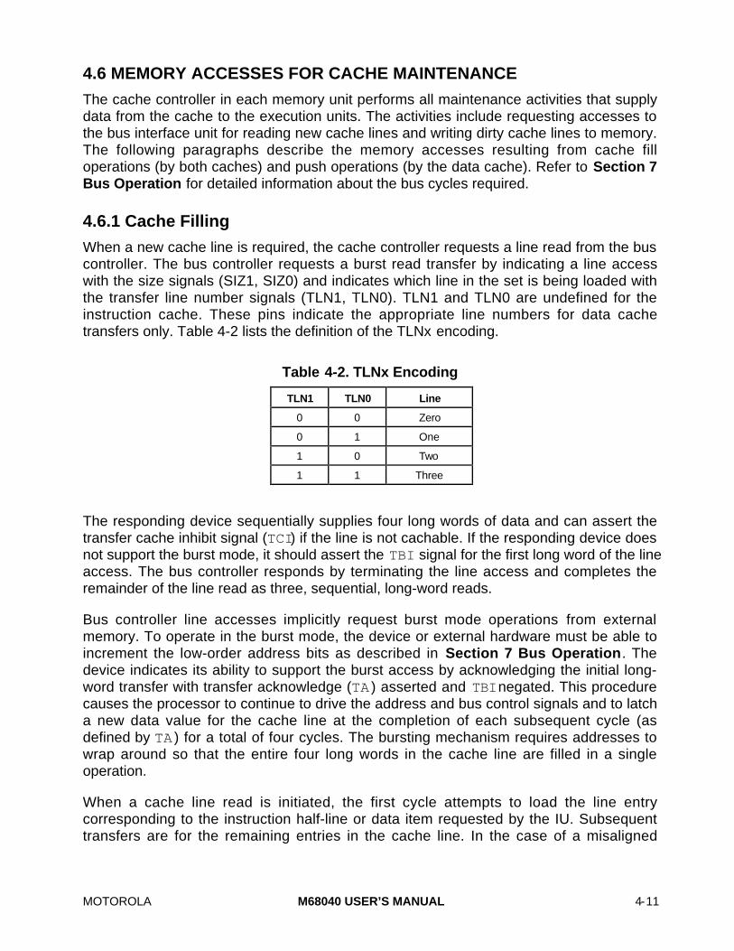
MOTOROLA M68040 USER’S MANUAL 4-11
4.6 MEMORY ACCESSES FOR CACHE MAINTENANCE
The cache controller in each memory unit performs all maintenance activities that supplydata from the cache to the execution units. The activities include requesting accesses tothe bus interface unit for reading new cache lines and writing dirty cache lines to memory.The following paragraphs describe the memory accesses resulting from cache filloperations (by both caches) and push operations (by the data cache). Refer to Section 7Bus Operation for detailed information about the bus cycles required.
4.6.1 Cache Filling
When a new cache line is required, the cache controller requests a line read from the buscontroller. The bus controller requests a burst read transfer by indicating a line accesswith the size signals (SIZ1, SIZ0) and indicates which line in the set is being loaded withthe transfer line number signals (TLN1, TLN0). TLN1 and TLN0 are undefined for theinstruction cache. These pins indicate the appropriate line numbers for data cachetransfers only. Table 4-2 lists the definition of the TLNx encoding.
Table 4-2. TLNx Encoding
TLN1 TLN0 Line
0 0 Zero
0 1 One
1 0 Two
1 1 Three
The responding device sequentially supplies four long words of data and can assert thetransfer cache inhibit signal (TCI) if the line is not cachable. If the responding device doesnot support the burst mode, it should assert the TBI signal for the first long word of the lineaccess. The bus controller responds by terminating the line access and completes theremainder of the line read as three, sequential, long-word reads.
Bus controller line accesses implicitly request burst mode operations from externalmemory. To operate in the burst mode, the device or external hardware must be able toincrement the low-order address bits as described in Section 7 Bus Operation. Thedevice indicates its ability to support the burst access by acknowledging the initial long-word transfer with transfer acknowledge (TA ) asserted and TBI negated. This procedurecauses the processor to continue to drive the address and bus control signals and to latcha new data value for the cache line at the completion of each subsequent cycle (asdefined by TA ) for a total of four cycles. The bursting mechanism requires addresses towrap around so that the entire four long words in the cache line are filled in a singleoperation.
When a cache line read is initiated, the first cycle attempts to load the line entrycorresponding to the instruction half-line or data item requested by the IU. Subsequenttransfers are for the remaining entries in the cache line. In the case of a misaligned
4-12 M68040 USER'S MANUAL MOTOROLA
access in which the operand spans two line entries, the first cycle corresponds to the lineentry containing the portion of the operand at the lower address.
The cache controller temporarily stores the data from each cycle in a line read buffer,where it is immediately available to the IU. If a misaligned access spans two entries in theline, the second portion of the operand is available to the IU as soon as the secondmemory cycle completes. A new IU access that hits the cache line being filled is alsosupplied data as soon as the required long word has been received from the buscontroller. During the period required to fill the buffer, other IU accesses that hit in thecache are supplied data. This is vertical for a short cache-inhibited code loop that is lessthan eight bytes in length. Subsequent interactions of the loop hit in the buffer, but appearto hit in the cache since there is no external bus activity associated with the reads.
The assertion of TCI during the first cycle of a burst read operation inhibits loading of thebuffered line into the cache, but it does not cause the burst transfer (or pseudo-bursttransfer if TBI is asserted with TCI) to be terminated early. The data placed in the buffer isaccessible by the IU until the last long word of the burst is transferred from the buscontroller, after which the contents of the buffer are invalidated without being copied intothe cache. The assertion of TCI is ignored during the second, third, or fourth cycle of aburst operation and is ignored for write operations.
A bus error occurring during a burst operation causes the burst operation to abort. If thebus error occurs during the first cycle of a burst, the data from the bus is ignored. If theaccess is a data cycle, exception processing proceeds immediately. If the cycle is for aninstruction prefetch, a bus error exception is pending. The bus error is processed only ifthe IU attempts to use either instruction word. Refer to Section 7 Bus Operation for moreinformation about pipeline operation.
For either cache, when a bus error occurs on the second cycle or later, the burst operationis aborted and the line buffer is invalidated. The processor may or may not take anexception, depending on the status of the pending data request. If the bus error cyclecontains a portion of a data operand that the processor is specifically waiting for (e.g., thesecond half of a misaligned operand), the processor immediately takes an exception.Otherwise, no exception occurs, and the cache line fill is repeated the next time datawithin the line is required. In the case of an instruction cache line fill, the data from theaborted cycle is completely ignored.
On the initial access of a line read, a retry (indicated by the assertion of TA and TEA )causes the bus controller to retry the bus cycle. However, a retry signaled during theremaining cycles of the line access (either burst or pseudo-burst) is recognized as a buserror, and the processor handles it as described in the previous paragraphs.
A cache inhibit or bus error on a line read can change the state of the line being replaced,even though the new line is not copied into the cache. Before loading a new line, thecache line being replaced is copied to the push buffer; if it is dirty, the cache line isinvalidated. If a cache inhibit or bus error occurs on a replacement line read, a dirty line isrestored to the cache from the push buffer. However, the line being replaced is notrestored in the cache if it was originally valid and the cache line remains invalid. If the line

MOTOROLA M68040 USER’S MANUAL 4-13
read resulting from a write miss in copyback mode is cache inhibited, the write accessmisses in the cache and writes through to memory.
4.6.2 Cache Pushes
When the cache controller selects a dirty data cache line for replacement, memory mustbe updated with the dirty data before the line is replaced. This occurs when a CPUSHinstruction execution explicitly selects the cache and when a cache inhibit access hits inthe cache. To reduce the requested data’s latency in the new line, the dirty line beingreplaced is temporarily placed in a push buffer while the new line is fetched from memory.When a line is allocated to the push buffer, an alternate bus master can snoop it, but theexecution units cannot access it. After the bus transfer for the new line successfullycompletes, the dirty cache line is copied back to memory, and the push buffer isinvalidated. If the operation to access the replacement line is abnormally terminated orsignaled as cache inhibited, the line in the push buffer is copied back into its originalposition in the cache, and the processor continues operation as described in the previousparagraphs.
The number of dirty long words in the line to be pushed determines the size of the pushtransfer on the bus, minimizing bus bandwidth required for the push. A single long word iswritten to memory using a long-word push transfer if it is dirty. A push transfer isdistinguished from a normal write transfer by an encoding of 000 on the transfer modifiersignals (TM2–TM0) for the push. Asserting TA and TEA retries the transfer; a bus-error -asserted TEA terminates it. If a bus error terminates a push transfer, the processorimmediately takes an exception.
A line containing two or more dirty long words is copied back to memory, using a line pushtransfer. For a line push, the bus controller requests a burst write transfer by indicating aline access with SIZ1 and SIZ0. The responding device sequentially accepts four longwords of data. If the responding device does not support the burst mode, it should assertTBI for the first long word of the line access. The bus controller responds by terminatingthe line access and completes the remainder of the line push as three, sequential, long-word writes. The first cycle of the burst can be retried, but the bus controller interprets aretry for any of the three remaining cycles as a bus error. If a bus error occurs in any cyclein the line push transfer, the processor immediately takes an exception.
A dirty cache line hit by a cache-inhibited access is pushed before the external bus accessoccurs. If the access is part of a locked transfer sequence for TAS, CAS, or CAS2operand accesses or translation table updates, the LOCK signal is also asserted for thepush access.
4.7 CACHE OPERATION SUMMARY
The instruction and data caches function independently when servicing access requestsfrom the IU. The following paragraphs discuss the operational details for the caches andpresent state diagrams depicting the cache line state transitions.

4-14 M68040 USER'S MANUAL MOTOROLA
4.7.1 Instruction Cache
The IU uses the instruction cache to store instruction prefetches as it requests them.Instruction prefetches are normally requested from sequential memory locations exceptwhen a change of program flow occurs (e.g., a branch taken) or when an instruction thatcan modify the status register (SR) is executed, in which case the instruction pipe isautomatically flushed and refilled. The instruction cache supports a line-based protocolthat allows individual cache lines to be in either the invalid or valid states.
For instruction prefetch requests that hit in the cache, the half-line selected by physicaladdress bit 3 is multiplexed onto the internal instruction data bus. When an access missesin the cache, the cache controller requests the line containing the required data frommemory and places it in the cache. If available, an invalid line is selected and updatedwith the tag and data from memory. The line state then changes from invalid to valid bysetting the V-bit. If all lines in the set are already valid, a pseudo-random replacementalgorithm is used to select one of the four cache lines replacing the tag and data contentsof the line with the new line information. Figure 4-5 illustrates the instruction-cache linestate transitions resulting from processor and snoop controller accesses. Transitions arelabeled with a capital letter, indicating the previous state, followed by a number indicatingthe specific case listed in Table 4-3.
INVALID VALID
I1-CPU READ MISS
I3–CINV/CPUSH V1–CPU READ MISS V2–CPU READ HIT
V3–CINV/CPUSH V5–SNOOP READ HIT V6–SNOOP WRITE HIT
Figure 4-5. Instruction-Cache Line State Diagram
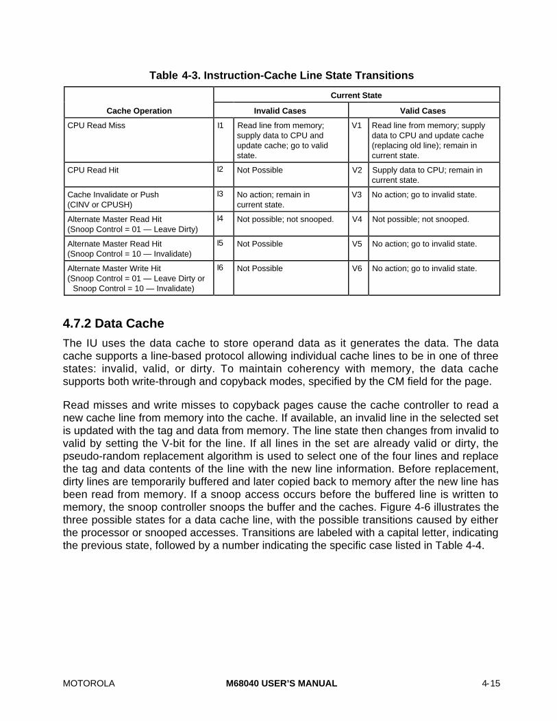
MOTOROLA M68040 USER’S MANUAL 4-15
Table 4-3. Instruction-Cache Line State Transitions
Current State
Cache Operation Invalid Cases Valid Cases
CPU Read Miss I1 Read line from memory;supply data to CPU andupdate cache; go to validstate.
V1 Read line from memory; supplydata to CPU and update cache(replacing old line); remain incurrent state.
CPU Read Hit I2 Not Possible V2 Supply data to CPU; remain incurrent state.
Cache Invalidate or Push(CINV or CPUSH)
I3 No action; remain incurrent state.
V3 No action; go to invalid state.
Alternate Master Read Hit(Snoop Control = 01 — Leave Dirty)
I4 Not possible; not snooped. V4 Not possible; not snooped.
Alternate Master Read Hit(Snoop Control = 10 — Invalidate)
I5 Not Possible V5 No action; go to invalid state.
Alternate Master Write Hit(Snoop Control = 01 — Leave Dirty or
Snoop Control = 10 — Invalidate)
I6 Not Possible V6 No action; go to invalid state.
4.7.2 Data Cache
The IU uses the data cache to store operand data as it generates the data. The datacache supports a line-based protocol allowing individual cache lines to be in one of threestates: invalid, valid, or dirty. To maintain coherency with memory, the data cachesupports both write-through and copyback modes, specified by the CM field for the page.
Read misses and write misses to copyback pages cause the cache controller to read anew cache line from memory into the cache. If available, an invalid line in the selected setis updated with the tag and data from memory. The line state then changes from invalid tovalid by setting the V-bit for the line. If all lines in the set are already valid or dirty, thepseudo-random replacement algorithm is used to select one of the four lines and replacethe tag and data contents of the line with the new line information. Before replacement,dirty lines are temporarily buffered and later copied back to memory after the new line hasbeen read from memory. If a snoop access occurs before the buffered line is written tomemory, the snoop controller snoops the buffer and the caches. Figure 4-6 illustrates thethree possible states for a data cache line, with the possible transitions caused by eitherthe processor or snooped accesses. Transitions are labeled with a capital letter, indicatingthe previous state, followed by a number indicating the specific case listed in Table 4-4.
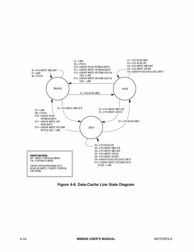
4-16 M68040 USER'S MANUAL MOTOROLA
VALID
DIRTY
INVALID
I4—CPU WRITE MISS/WT I7—CINV I8—CPUSH
I3—CPU WRITE MISS/CB
V1—CPU READ MISS V2—CPU READ HIT V4—CPU WRITE MISS/WT V6—CPU WRITE HIT/WT V9—SNOOP READ HIT/LEAVE DIRTY
ABBREVIATIONS:WT—WRITE-THROUGH MODECB—COPYBACK MODE
SNOOP OPERATION INDICATES:READ OR WRITE / SNOOP CONTROL ENCODING
I1—CPU READ MISS
V7—CINV V8—CPUSH V10—SNOOP READ HIT/INVALIDATE V11—SNOOP WRITE HIT/INVALIDATE V12—SNOOP WRITE HIT/SINK DATA & SIZE = LINE V13—SNOOP WRITE HIT/SINK DATA & SIZE = LINE
D2—CPU READ HIT D3—CPU WRITE MISS/CB D4—CPU WRITE MISS/WT D5—CPU WRITE HIT/CB D6—CPU WRITE HIT/WT D9—SNOOP READ HIT/LEAVE DIRTY D12—SNOOP WRITE HIT/SINK DATA & SIZE = LINE
D7—CINV D8—CPUSH D10—SNOOP READ HIT/INVALIDATE D11—SNOOP WRITE HIT/ INVALIDATE D13—SNOOP WRITE HIT/SINK DATA & SIZE = LINE
V3—CPU WRITE MISS/CB V5—CPU WRITE HIT/CB
D1—CPU READ MISS
Figure 4-6. Data-Cache Line State Diagram

MOTOROLA M68040 USER’S MANUAL 4-17
Table 4-4. Data-Cache Line State Transitions
Current State
Cache Operation Invalid Cases Valid Cases Dirty Cases
CPU Read Miss I1 Read line frommemory; supply datato CPU and updatecache; go to validstate.
V1 Read line frommemory; supply datato CPU and updatecache (replacing oldline); remain in currentstate.
D1 Buffer dirty cache line;read new line frommemory; supply datato CPU and updatecache; write buffereddirty data to memory;go to valid state.
CPU Read Hit I2 Not Possible V2 Supply data to CPU;remain in current state.
D2 Supply data to CPU;remain in current state.
CPU Write Miss(Copyback)
I3 Read line frommemory into cache;write data to cache;set Dn bits of modifiedlong words; go to dirtystate.
V3 Read line frommemory into cache(replacing old line);write data to cacheand set Dn bits; go todirty state.
D3 Buffer dirty cache line;read new line frommemory; write data tocache and set Dn bits;write buffered dirtydata to memory;remain in current state.
CPU Write Miss(Write-through)
I4 Write data to memory;remain in current state.
V4 Write data to memory;remain in current state.
D4 Write data to memory;remain in current state(see note).
CPU Write Hit(Copyback)
I5 Not Possible V5 Write data into cache;set Dn bits of modifiedlong words; go to dirtystate.
D5 Write data in cache;set Dn bits of modifiedlong words; remain incurrent state.
CPU Write Hit(Write-through)
I6 Not Possible V6 Write data to cache;write data to memory;remain in current state.
D6 Write data into cache(no change to Dn bits);write data to memory;remain in current state(see note).
Cache Invalidate(CINV)
I7 No action; remain incurrent state.
V7 No action; go to invalidstate.
D7 No action (dirty datalost); go to invalidstate.
Cache Push(CPUSH)
I8 No action; remain incurrent state.
V8 No action; go to invalidstate.
D8 Write dirty data tomemory; go to invalidstate.
Alternate Master Read Hit(Snoop Control = 01— Leave Dirty)
I9 Not Possible V9 No action; remain incurrent state.
D9 Inhibit memory andsource data; remain incurrent state.
NOTE: Dirty state transitions D4 and D6 are the result of a system programming error and should be avoided eventhough they are technically valid.

4-18 M68040 USER'S MANUAL MOTOROLA
Table 4-4. Data-Cache Line State Transitions (Continued)
Current State
Cache Operation Invalid Cases Valid Cases Dirty Cases
Alternate Master Read Hit(Snoop Control = 10— Invalidate)
I10 Not Possible V10 No action; go to invalidstate.
D10 Inhibit memory andsource data; go toinvalid state
Alternate Master Write Hit(Snoop Control = 10—Invalidate)
I11 Not Possible V11 No action; go to invalidstate.
D11 No action; go to invalidstate.
Alternate Master Write Hit(Snoop Control = 01— Sink Data andSize ≠ Line)
I12 Not Possible V12 No action; go to invalidstate.
D12 Inhibit memory andsink data; set Dn bitsof modified longwords; remain incurrent state.
Alternate Master Write Hit(Snoop Control = 01— Sink Data andSize = Line)
I13 Not Possible V13 No action; go to invalidstate.
D13 No action; go to invalidstate.
MOTOROLA M68040 USER’S MANUAL 5-1
SECTION 5SIGNAL DESCRIPTION
This section contains brief descriptions of the input and output signals in their functionalgroups (see Figure 5-1). Each signal’s function is briefly explained, referencing othersections that contain detailed information about the signal and related operations. Table5-1 lists the signal names, mnemonics, and functional descriptions of the input and outputsignals for the M68040. Timing specifications for these signals can be found in Section 11MC68040 Electrical and Thermal Characteristics.
NOTES
Assertion and negation are used to specify forcing a signal to aparticular state. Assertion and assert refer to a signal that isactive or true. Negation and negate refer to a signal that isinactive or false. These terms are used independent of thevoltage level (high or low) that they represent.
For the MC68040V, MC68LC040, MC68EC040, andMC68EC040V ignore all references to the floating-point unit(FPU). For the MC68EC040 and MC68EC040V only, ignore allreferences to the memory management unit (MMU). Some pinnames are different on these parts; please refer to theappropriate appendix in the back of this book for moreinformation.
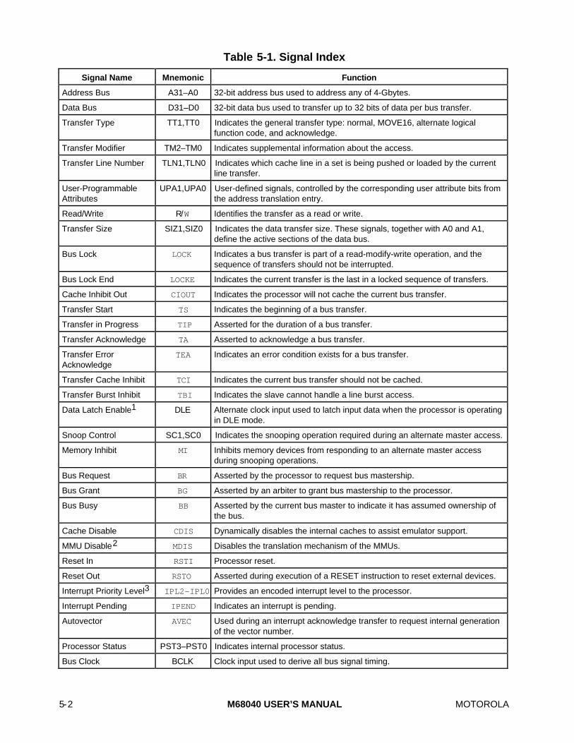
5-2 M68040 USER’S MANUAL MOTOROLA
Table 5-1. Signal Index
Signal Name Mnemonic Function
Address Bus A31–A0 32-bit address bus used to address any of 4-Gbytes.
Data Bus D31–D0 32-bit data bus used to transfer up to 32 bits of data per bus transfer.
Transfer Type TT1,TT0 Indicates the general transfer type: normal, MOVE16, alternate logicalfunction code, and acknowledge.
Transfer Modifier TM2–TM0 Indicates supplemental information about the access.
Transfer Line Number TLN1,TLN0 Indicates which cache line in a set is being pushed or loaded by the currentline transfer.
User-ProgrammableAttributes
UPA1,UPA0 User-defined signals, controlled by the corresponding user attribute bits fromthe address translation entry.
Read/Write R/W Identifies the transfer as a read or write.
Transfer Size SIZ1,SIZ0 Indicates the data transfer size. These signals, together with A0 and A1,define the active sections of the data bus.
Bus Lock LOCK Indicates a bus transfer is part of a read-modify-write operation, and thesequence of transfers should not be interrupted.
Bus Lock End LOCKE Indicates the current transfer is the last in a locked sequence of transfers.
Cache Inhibit Out CIOUT Indicates the processor will not cache the current bus transfer.
Transfer Start TS Indicates the beginning of a bus transfer.
Transfer in Progress TIP Asserted for the duration of a bus transfer.
Transfer Acknowledge TA Asserted to acknowledge a bus transfer.
Transfer ErrorAcknowledge
TEA Indicates an error condition exists for a bus transfer.
Transfer Cache Inhibit TCI Indicates the current bus transfer should not be cached.
Transfer Burst Inhibit TBI Indicates the slave cannot handle a line burst access.
Data Latch Enable1 DLE Alternate clock input used to latch input data when the processor is operatingin DLE mode.
Snoop Control SC1,SC0 Indicates the snooping operation required during an alternate master access.
Memory Inhibit MI Inhibits memory devices from responding to an alternate master accessduring snooping operations.
Bus Request BR Asserted by the processor to request bus mastership.
Bus Grant BG Asserted by an arbiter to grant bus mastership to the processor.
Bus Busy BB Asserted by the current bus master to indicate it has assumed ownership ofthe bus.
Cache Disable CDIS Dynamically disables the internal caches to assist emulator support.
MMU Disable2 MDIS Disables the translation mechanism of the MMUs.
Reset In RSTI Processor reset.
Reset Out RSTO Asserted during execution of a RESET instruction to reset external devices.
Interrupt Priority Level3 IPL2—IPL0 Provides an encoded interrupt level to the processor.
Interrupt Pending IPEND Indicates an interrupt is pending.
Autovector AVEC Used during an interrupt acknowledge transfer to request internal generationof the vector number.
Processor Status PST3–PST0 Indicates internal processor status.
Bus Clock BCLK Clock input used to derive all bus signal timing.

MOTOROLA M68040 USER’S MANUAL 5-3
Table 5-1. Signal Index (Continued)
Signal Name Mnemonic Function
Processor Clock PCLK4 Clock input used for internal logic timing. The PCLK frequency is exactly 2 ×the BCLK frequency.
Test Clock TCK Clock signal for the IEEE P1149.1 Test Access Port (TAP).
Test Mode Select TMS Selects the principle operations of the test-support circuitry.
Test Data Input TDI Serial data input for the TAP.
Test Data Output TDO Serial data output for the TAP.
Test Reset TRST4 Provides an asynchronous reset of the TAP controller.
Power Supply VCC Power supply.
Ground GND Ground connection.
NOTES:1. This signal is only available on the MC68040.2. This signal is not available on the MC68EC040 and the MC68EC040V.3. These signals are different on power-up for the MC68LC040 and MC68EC040.4. These signals are not available on the MC68040V and MC68EC040V.
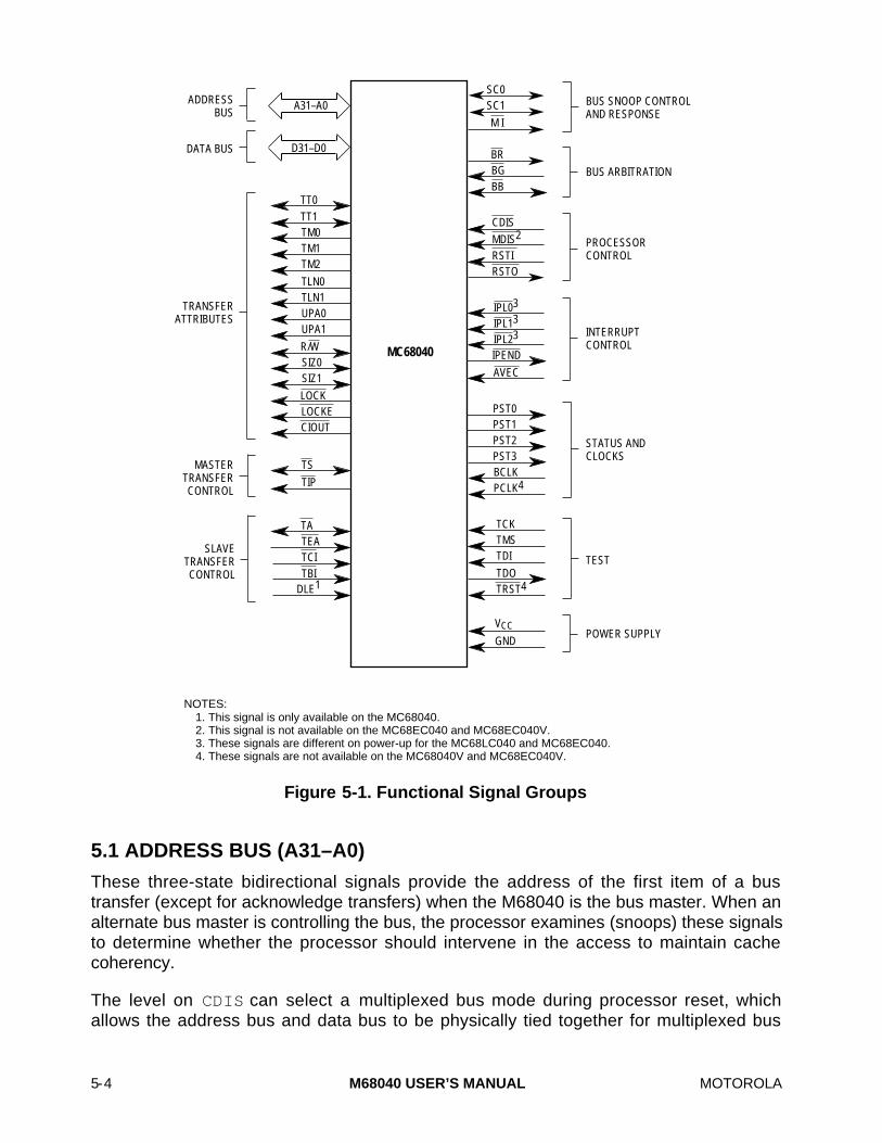
5-4 M68040 USER’S MANUAL MOTOROLA
MC68040
VCC
GND
BUS ARBITRATIONBGBR
BB
BUS SNOOP CONTROL AND RESPONSE
M I
INTERRUPT CONTROL
IPL03
AVEC
IPEND
PROCESSOR CONTROL
CDIS
RSTIRSTO
PCLK4BCLK
TEST
TRST4
TMSTCK
TDI
POWER SUPPLY
TDO
SC0SC1
IPL13
IPL23
STATUS AND CLOCKS
PST0PST1PST2
DATA BUS D31–D0
TRANSFER ATTRIBUTES
MASTER TRANSFER CONTROL
A31–A0ADDRESS BUS
TS
TIP
TCISLAVE
TRANSFER CONTROL
TEA
TBI
R/W
LOCKECIOUT
TT0TT1TM0TM1TM2
TLN0TLN1UPA0UPA1
SIZ0SIZ1
LOCK
TA
DLE1
MDIS2
1. This signal is only available on the MC68040. 2. This signal is not available on the MC68EC040 and MC68EC040V. 3. These signals are different on power-up for the MC68LC040 and MC68EC040. 4. These signals are not available on the MC68040V and MC68EC040V.
NOTES:
PST3
Figure 5-1. Functional Signal Groups
5.1 ADDRESS BUS (A31–A0)
These three-state bidirectional signals provide the address of the first item of a bustransfer (except for acknowledge transfers) when the M68040 is the bus master. When analternate bus master is controlling the bus, the processor examines (snoops) these signalsto determine whether the processor should intervene in the access to maintain cachecoherency.
The level on CDIS can select a multiplexed bus mode during processor reset, whichallows the address bus and data bus to be physically tied together for multiplexed bus

MOTOROLA M68040 USER’S MANUAL 5-5
applications. Refer to Section 7 Bus Operation for detailed information about therelationship of the address bus to bus operation and the multiplexed bus mode. Refer toAppendix A MC68LC040 and Appendix B MC68EC040 for details concerning the CDISlevel and multiplexed bus mode.
5.2 DATA BUS (D31–D0)
These three-state bidirectional signals provide the general-purpose data path between theM68040 and all other devices. The data bus can transfer 8, 16, or 32 bits of data per bustransfer. During a burst transfer, the data lines are time-multiplexed to carry all 128 bits ofthe burst request using four 32-bit transfers.
The level on CDIS can select a multiplexed bus mode during processor reset, whichallows the data bus and address bus to be physically tied together for multiplexed busapplications. The level on MDIS can select a data latch mode during processor reset,which allows the memory interface to specify when the processor should latch input datathrough the DLE signal. Section 7 Bus Operation provides detailed information about therelationship of the data bus to bus operation, the multiplexed bus mode, and the data latchmode. Refer to Appendix A MC68LC040 and Appendix B MC68EC040 for detailsconcerning the CDIS level and multiplexed bus mode.
5.3 TRANSFER ATTRIBUTE SIGNALS
The following paragraphs describe the transfer attribute signals, which provide additionalinformation about the bus transfer. Refer to Section 7 Bus Operation for detailedinformation about the relationship of the transfer attribute signals to bus operation.
5.3.1 Transfer Type (TT1, TT0)
The processor drives these three-state bidirectional signals to indicate the type of accessfor the current bus transfer. During bus transfers by an alternate bus master, theprocessor samples these signals to determine if it should snoop the transfer; only normaland MOVE16 accesses can be snooped. Table 5-2 lists the definition of the transfer-typeencoding. The acknowledge access (TT1 = 1 and TT0 = 1) is used for both interrupt andbreakpoint acknowledge transfers, and for LPSTOP broadcast cycles on the MC68040Vand MC68EC040V.
Table 5-2. Transfer-Type Encoding
TT1 TT0 Transfer Type
0 0 Normal Access
0 1 MOVE16 Access
1 0 Alternate Logical Function Code Access
1 1 Acknowledge Access

5-6 M68040 USER’S MANUAL MOTOROLA
5.3.2 Transfer Modifier (TM2–TM0)
These three-state outputs provide supplemental information for each transfer type. Table5-3 lists the encoding for normal and MOVE16 transfers, and Table 5-4 lists the encodingfor alternate access transfers. For interrupt acknowledge transfers, the TMx signals carrythe interrupt level being acknowledged; for breakpoint acknowledge transfers andLPSTOP broadcast cycles on the MC68040V and MC68EC040V, the TMx signals are low.When the M68040 is not the bus master, the TMx signals are set to a high-impedancestate.
Table 5-3. Normal and MOVE16 AccessTransfer Modifier Encoding
TM2 TM1 TM0 Transfer Modifier
0 0 0 Data Cache Push Access
0 0 1 User Data Access*
0 1 0 User Code Access
0 1 1 MMU Table Search Data Access
1 0 0 MMU Table Search Code Access
1 0 1 Supervisor Data Access*
1 1 0 Supervisor Code Access
1 1 1 Reserved
* MOVE16 accesses use only these encodings.
Table 5-4. Alternate Access Transfer Modifier Encoding
TM2 TM1 TM0 Transfer Modifier
0 0 0 Logical Function Code 0
0 0 1 Reserved
0 1 0 Reserved
0 1 1 Logical Function Code 3
1 0 0 Logical Function Code 4
1 0 1 Reserved
1 1 0 Reserved
1 1 1 Logical Function Code 7
5.3.3 Transfer Line Number (TLN1, TLN0)
These three-state outputs indicate which line in the set of four data cache lines is beingaccessed for normal push and line data read accesses. TLNx signals are undefined for allother accesses to instruction space and are placed in a high-impedance state when theprocessor relinquishes the bus.

MOTOROLA M68040 USER’S MANUAL 5-7
The TLNx signals can be used in high-performance systems to build an external snoopfilter with a duplicate set of cache tags. The TLNx signals and address bus provide adirect indication of the state of the data caches and can be used to help maintain theduplicate tag store. The TLNx pins do not indicate the correct TLN number when aninstruction cache burst fill occurs.
5.3.4 User-Programmable Attributes (UPA1, UPA0)
The UPAx signals are three-state outputs. If they match the logical address, the user-programmable attribute bits in the address translation entry or the transparent translationregister determine the UPAx signal level. These signals are only for normal code, data,and MOVE16 accesses. For all other accesses, including table search and cache linepush accesses, which may result from a normal access, the UPAx signals are zero. If thetransparent translation register and the memory management unit are disabled, the UPAxsignals are also zero. When the M68040 is not the bus master, these signals are set to ahigh-impedance state.
5.3.5 Read/Write (R/W)
This bidirectional three-state signal defines the data transfer direction for the current buscycle. A high level indicates a read cycle, and a low level indicates a write cycle. The bussnoop controller examines this signal when the processor is not the bus master.
5.3.6 Transfer Size (SIZ1, SIZ0)
These bidirectional three-state signals indicate the data size for the bus transfer. The bussnoop controller examines this signal when the processor is not the bus master. Refer toSection 7 Bus Operation for more information on the encoding of these signals.
5.3.7 Lock (LOCK )
This three-state output indicates that the current transfer is part of a sequence of lockedtransfers for a read-modify-write operation. The external arbiter can use LOCK to preventan alternate bus master from gaining control of the bus and accessing the same operandbetween processor accesses for the locked sequence of transfers. Although LOCKindicates that the processor requests the bus be locked, the processor will give up the busif the external arbiter negates the BG signal. When the M68040 is not the bus master, theLOCK signal is set to a high-impedance state. LOCK drives high before three-stating.Refer to Section 7 Bus Operation for information on locked transfers.
5.3.8 Lock End (LOCKE)
This three-state output indicates that the current transfer is the last in a sequence oflocked transfers for a read-modify-write operation. The external arbiter can use LOCKE tosupport arbitration between unrelated locked transfer sequences while still maintaining theindivisible nature of each read-modify-write operation. When the M68040 is not the busmaster, the LOCKE signal is set to a high-impedance state. LOCKE drives high before

5-8 M68040 USER’S MANUAL MOTOROLA
three-stating. Do not use LOCKE if it is possible to retry the last write of a read-write-modify operation.
5.3.9 Cache Inhibit Out (CIOUT)
This three-state output reflects the state of the cache mode field in one of the addresstranslation caches and is asserted for accesses to noncachable pages to indicate that anexternal cache should ignore the bus transfer. When the referenced logical address iswithin an area specified for transparent translation, the cache mode field of theappropriate transparent translation register controls the state of CIOUT. Refer to Section3 Memory Management Unit (Except MC68EC040 and MC68EC040V) for moreinformation about the address translation caches and transparent translation. When theM68040 is not the bus master, the CIOUT signal is set to a high-impedance state.
5.4 BUS TRANSFER CONTROL SIGNALS
The following signals provide control functions for bus transfers. Refer to Section 7 BusOperation for detailed information about the relationship of the bus transfer controlsignals to bus operation.
5.4.1 Transfer Start (TS)
The processor asserts this three-state bidirectional signal for one clock period to indicatethe start of each transfer. During alternate bus master accesses, the processor monitorsthis signal to detect the start of each transfer to be snooped.
5.4.2 Transfer in Progress (TIP)
This three-state output is asserted to indicate that a bus transfer is in progress and isnegated during idle bus cycles if the bus is still granted to the processor. When theprocessor loses the bus, TIP negates after completion of the current transfer and goes toa high-impedance state. Note that TIP is kept asserted on back-to-back bus cycles.
5.4.3 Transfer Acknowledge (TA)
This three-state bidirectional signal indicates the completion of a requested data transferoperation. During transfers by the M68040, TA is an input signal from the referenced slavedevice indicating completion of the transfer. During alternate bus master accesses, TA isnormally three-stated to allow the referenced slave device to respond, and the M68040samples it to detect the completion of each bus transfer. The M68040 can inhibit memoryand intervene in the access to source or sink data in its internal caches by asserting TA toacknowledge the data transfer. This capability applies to alternate bus master accessesthat reference modified (dirty) data in the M68040 caches.
5.4.4 Transfer Error Acknowledge (TEA)
The current slave asserts this input signal to indicate an error condition for the bustransaction. When asserted with TA, this signal indicates that the processor should retry

MOTOROLA M68040 USER’S MANUAL 5-9
the access. During alternate bus master accesses, the M68040 samples TEA to detectcompletion of each bus transfer.
5.4.5 Transfer Cache Inhibit (TCI)
This input signal inhibits read data from being loaded into the M68040 instruction or datacaches. TCI is ignored during all writes and after the first data transfer for both burst linereads and burst-inhibited line reads. TCI is also ignored during all alternate bus mastertransfers.
5.4.6 Transfer Burst Inhibit (TBI)
This input signal indicates to the processor that the accessed device cannot support burstmode accesses and that the requested line transfer should be divided into individual long-word transfers. Asserting TBI with TA terminates the first data transfer of a line access,which causes the processor to terminate the burst and access the remaining data for theline as three successive long-word transfers. During alternate bus master accesses, theM68040 samples the TBI to detect completion of each bus transfer.
5.5 SNOOP CONTROL SIGNALS
The following signals control the operation of the M68040 on-chip snoop logic. Section 4Instruction and Data Caches provides information about the relationship of the snoopcontrol signals to the caches, and Section 7 Bus Operation discusses the relationship ofthese signals to bus operation.
5.5.1 Snoop Control (SC1, SC0)
These input signals specify the snoop operation to be performed by the M68040 for analternate bus master transfer. If the M68040 is allowed to snoop an alternate bus masterread transfer, it can intervene in the access to supply data from its data cache when thememory copy is stale, ensuring that the alternate bus master receives valid data. Writesby an alternate bus master can also be snooped to either update the M68040 internal datacache with the new data or invalidate the matching cache lines, ensuring that subsequentM68040 reads access valid data. These signals are ignored when the processor is the busmaster.
5.5.2 Memory Inhibit (MI)
This output signal prevents an alternate bus master from accessing possibly stale data inmemory while the M68040 is unable to respond. MI is asserted during reset preventingexternal memory from responding. When the SCx signals indicate an access should besnooped, the M68040 keeps MI asserted until it determines if intervention in the access isrequired. If no intervention is required, MI is negated and memory is allowed to respond tocomplete the access. Otherwise, MI remains asserted and the M68040 completes thetransfer as a slave. It updates its caches on a write or supplies data to the alternate busmaster on a read. MI is negated when the M68040 is the bus master. During a snoop

5-10 M68040 USER’S MANUAL MOTOROLA
cycle, the M68040 ignores all TA and TEA assertions while MI is asserted; when RSTI isasserted, MI is asserted.
5.6 ARBITRATION SIGNALS
The following control signals support requests to an external arbiter to become the busmaster. Refer to Section 7 Bus Operation for detailed information about the relationshipof the arbitration signals to bus operation.
5.6.1 Bus Request (BR)
This output signal indicates to the external arbiter that the processor needs to become busmaster for one or more bus transfers. BR is negated when the M68040 begins an accessto the external bus with no other accesses pending, and BR remains negated until anotheraccess is required. There are some situations in which the M68040 asserts BR and thennegates it without having run bus transfers; this is a disregard request condition. Refer toSection 7 Bus Operation for details about this state.
5.6.2 Bus Grant (BG )
This input signal from an external arbiter indicates that the bus is available to the M68040as soon as the current bus access completes. BG must be asserted and BB must benegated (indicating the bus is free) before the M68040 assumes ownership of the bus.
5.6.3 Bus Busy (BB)
This three-state bidirectional signal indicates that the bus is currently owned. BB ismonitored as a processor input to determine when a alternate bus master has releasedcontrol of the bus. BG must be asserted and BB must be negated (indicating the bus isfree) before the M68040 asserts BB as an output to assume ownership of the bus. Theprocessor keeps BB asserted until the external arbiter negates BG and the processorcompletes the bus transfer in progress. When releasing the bus, the processor negatesBB , then sets it to a high-impedance state for use again as an input.
5.7 PROCESSOR CONTROL SIGNALS
The following signals control disabling caches and memory management units (MMUs)and support processor and external device initialization.
5.7.1 Cache Disable (CDIS)
CDIS dynamically disables the on-chip caches on the next internal cache accessboundary. CDIS does not flush the data and instruction caches; entries remain unalteredand become available after CDIS is negated. The assertion of CDIS does not affectsnooping. During a processor reset, the level on CDIS is latched and used to select thenormal bus mode (CDIS high) or multiplexed bus mode (CDIS low). Refer to Section 4Instruction and Data Caches for information about the caches and to Section 7 BusOperation for information about the multiplexed bus mode. Refer to Appendix E

MOTOROLA M68040 USER’S MANUAL 5-11
MC68040 Floating-Point Emulation (MC68040FPSP) for descriptions of emulator use ofthis signal.
5.7.2 Reset In (RSTI)
This input signal causes the M68040 to enter reset exception processing. The RSTI signalis an asynchronous input that is internally synchronized to the next rising edge of theBCLK signal. All three-state signals are set to the high-impedance state, and all outputs,except MI, are negated when RSTI is recognized. The assertion of RSTI does not affectthe test pins. Refer to Section 7 Bus Operation for a description of reset operation and toSection 8 Exception Processing for information about the reset exception.
5.7.3 Reset Out (RSTO)
The M68040 asserts this output during execution of the RESET instruction to initializeexternal devices. Refer to Section 7 Bus Operation for a description of reset out busoperation.
5.8 INTERRUPT CONTROL SIGNALS
The following signals control the interrupt functions.
5.8.1 Interrupt Priority Level (IPL2–IPL0)
These input signals provide an indication of an interrupt condition and the encoding of theinterrupt level from a peripheral or external prioritizing circuitry. IPL2 is the most significantbit of the level number. For example, since the IPL signals are active low, IPL2–IPL0 = $5corresponds to an interrupt request at interrupt priority level 2.
During a processor reset, the levels on the IPL lines are latched and used to select theoutput driver characteristics for three signal groups listed in Table 5-5. Refer to Section 8Exception Processing for information on interrupts and to Section 11 MC68040Electrical and Thermal Characteristics for information on driver characteristics. Refer toAppendix A MC68LC040 and Appendix B MC68EC040 for how these signals aredifferent on power-up.
Table 5-5. Output Driver Control Groups
Signal Output Buffers Controlled
IPL2 Data-Bus: D31–D0
IPL1 Address Bus and Transfer Attributes:A31–A0, CIOUT, LOCK, LOCKE , R/W, SIZ1–SIZ0,TLN1–TLN0, TM2–TM0, TT1–TT0, UPA1–UPA0
IPL0 Miscellaneous Control Signals:BB, BR , IPEND, MI, PST3–PST0, RSTO , TA, TDO, TIP, TS
NOTE: High input level = small buffers enabled; low input level = large buffers enabled.

5-12 M68040 USER’S MANUAL MOTOROLA
5.8.2 Interrupt Pending Status (IPEND)
This output signal indicates that an interrupt request has been recognized internally andexceeds the current interrupt priority mask in the status register (SR). External devices(other bus masters) can use IPEND to predict processor operation on the next instructionboundaries. IPEND is not intended for use as an interrupt acknowledge to externalperipheral devices. Refer to Section 7 Bus Operation for bus information related tointerrupts and to Section 8 Exception Processing for interrupt information.
5.8.3 Autovector (AVEC )
This input signal is asserted with TA during an interrupt acknowledge transfer to requestinternal generation of the vector number. Refer to Section 7 Bus Operation for moreinformation about automatic vectors.
5.9 STATUS AND CLOCK SIGNALS
The following paragraphs explain the signals that provide timing, test control, and theinternal processor status.
5.9.1 Processor Status (PST3–PST0)
These outputs indicate the internal execution unit’s status. The timing is synchronous withBCLK, and the status may have nothing to do with the current bus transfer. The PSTxsignal is updated depending on the type of PSTx encoding. There are two classes ofPSTx encodings. The first class is associated with instruction boundaries, and the secondclass indicates the processor’s present status. Table 5-6 lists the definition of theencodings.
The encodings 0, 8, 4, 5, C, D, E, and F indicate the present status and do not reflect aspecific stage of the pipe. These encodings persist as long as the processor stays in theindicated state. The default encoding 0 (user) or 8 (supervisor) is indicated if none of theabove conditions apply. The encodings 1, 2, 3, 9, A, and B belong to the first class ofPSTx encoding. This class indicates that the instruction is in its last instruction executionstage. These encodings exist for only one BCLK period per instruction and are mutuallyexclusive.

MOTOROLA M68040 USER’S MANUAL 5-13
Table 5-6. Processor Status Encoding
Hex PST3 PST2 PST1 PST0 Internal Status
0 0 0 0 0 User, Start/Continue Current Instruction
1 0 0 0 1 User, End Current Instruction
2 0 0 1 0 User, Branch Not Taken/End Current Instruction
3 0 0 1 1 User, Branch Taken/End Current Instruction
4 0 1 0 0 User, Table Search
5 0 1 0 1 Halted State (Double Bus Fault)
6 0 1 1 0 Low-Power Stop Mode (Supervisor Instruction)*
7 0 1 1 1 Reserved
8 1 0 0 0 Supervisor, Start/Continue Current Instruction
9 1 0 0 1 Supervisor, End Current Instruction
A 1 0 1 0 Supervisor, Branch Not Taken/End Current Instruction
B 1 0 1 1 Supervisor, Branch Taken/End Current Instruction
C 1 1 0 0 Supervisor, Table Search
D 1 1 0 1 Stopped State (Supervisor Instruction)
E 1 1 1 0 RTE Executing
F 1 1 1 1 Exception Stacking
NOTE: *MC68040V and MC68EC040V only.
When a ‘branch taken/end current instruction’ is indicated, it means that a change ofinstruction flow is pending. Along with the following instructions, an exception stacking(encoding F) sequence is ended with the ‘supervisor, branch taken/end current instruction’encoding as though it were a virtual JMP instruction. This includes all the possibleexceptions listed in the processor’s vector table. Instructions that cause a ‘branchtaken/end current instruction’ encoding when they are executed are as follows:
ANDI to SR DBcc (Taken) MOVE to SR RTD
Bcc (Taken) FBcc (Taken) MOVE USP RTE
BRA FDBcc (Always) MOVEC RTR
BSR FMOVEM Rc,MRn MOVES RTS
CAS FMOVEM FPm,MRn NOP STOP
CAS2 FSAVE ORI to SR TAS
CINV JMP PFLUSH
CPUSH JSR PTEST
The Bcc (not taken) and DBcc (not taken) are the only instructions that cause a ‘branchnot taken/end current instruction’ encoding. Note that the FBcc (not taken) is not includedin this category. The FBcc (not taken) instruction ends with an ‘end current instruction’encoding. All other instructions and conditions end with the ‘end current instruction’encoding. For instance, if the processor is running back-to-back single clock instructions,the encoding ‘end current instruction’ remains asserted for as many clock cycles asinstructions.

5-14 M68040 USER’S MANUAL MOTOROLA
The following examples are for PSTx encodings:
1. An access error terminates an instruction such that the instruction execution stage isnot reached. In this case, an ‘end current instruction’ is not indicated. Exceptionprocessing starts, the exception stacking status is indicated, and then the virtualJMP causes the ‘supervisor, branch taken/end current instruction’ encoding.
2. An FTRAPcc that does not take an exception ending with the ‘end currentinstruction’ encoding. The exception stacking status is indicated and then reachesthe ‘supervisor, branch taken/end current instruction’ encoding if the FTRAPcc endsin an exception.
3. Two simultaneous interrupt exception processing sequences follow an ADDinstruction. The ADD instruction ends with ‘end current instruction’, followed byexception stacking, followed by ‘branch taken/end current instruction’, followed byexception stacking, followed by ‘branch taken/end current instruction’.
4. An RTE instruction follows an ADD instruction. The ‘end current instruction’ isfollowed by RTE executing followed by a branch taken/end current instruction.
5.9.2 Bus Clock (BCLK)
This input signal is used as a reference for all bus timing. It is a TTL-compatible signal andcannot be gated off. Refer to Section 11 MC68040 Electrical and ThermalCharacteristics for electrical specifications.
5.9.3 Processor Clock (PCLK)—Not on MC68040V and MC68EC040V
PCLK is used to derive all internal timing. This clock is also TTL compatible and cannot begated off. Refer to Section 11 MC68040 Electrical and Thermal Characteristics forelectrical specifications.
5.10 MMU DISABLE (MDIS)—NOT ON MC68EC040
The MMU disable signal dynamically disables the translation of addresses by the MMUs.The assertion of MDIS does not flush the address translation caches (ATCs); ATC entriesbecome available again when MDIS is negated. During a processor reset, the level onMDIS is latched and used to select the normal data latch mode (MDIS high) or DLE mode(MDIS low). Refer to Section 3 Memory Management Unit (Except MC68EC040 andMC68EC040V) for a description of address translation and to Section 7 Bus Operationfor information about DLE mode.
5.11 DATA LATCH ENABLE (DLE)—ONLY ON MC68040
This input signal is used in DLE mode to latch the input data bus on read transfers. DLEmode can be used to support asynchronous memory interfaces by allowing the interfaceto specify when data should be latched instead of requiring data to be valid on the risingedge of BCLK.

MOTOROLA M68040 USER’S MANUAL 5-15
5.12 TEST SIGNALS
The M68040 includes dedicated user-accessible test logic that is fully compatible with theIEEE 1149.1 Standard Test Access Port and Boundary Scan Architecture. Problemsassociated with testing high-density circuit boards have led to the development of thisstandard under the IEEE Test Technology Committee and Joint Test Action Group (JTAG)sponsorship. The M68040 implementation supports circuit board test strategies based onthis standard. However, the JTAG interface is not intended to provide an in-circuit test toverify M68040 operations; therefore, it is impossible to test M68040 operations using thisinterface. Section 6 IEEE 1149.1 Test Access Port (JTAG) describes the M68040implementation of the IEEE 1149.1 and is intended to be used with the supporting IEEEdocument.
5.12.1 Test Clock (TCK)
This input signal is used as a dedicated clock for the test logic. Since clocking of the testlogic is independent of the normal operation of the MC68040, several other componentson a board can share a common test clock with the processor even though eachcomponent may operate from a different system clock. The design of the test logic allowsthe test clock to run at low frequencies, or to be gated off entirely as required for testpurposes.
5.12.2 Test Mode Select (TMS)
This input signal is decoded by the TAP controller and distinguishes the principleoperationas of the test support circuitry.
5.12.3 Test Data In (TDI)
This input signal provides a serial data input to the TAP.
5.12.4 Test Data Out (TDO)
This three-state output signal provides a serial data output from the TAP. The TDO outputcan be placed in a high-impedance mode to allow parallel connection of board-level testdata paths.
5.12.5 Test Reset (TRST )—Not on MC68040V and MC68EC040V
This input signal provides an asynchronous reset of the TAP controller.
5.13 POWER SUPPLY CONNECTIONS
The M68040 requires connection to a VCC power supply, positive with respect to ground.The VCC and ground connections are grouped to supply adequate current to the varioussections of the processor. Section 12 Ordering Information and Mechanical Datadescribes the groupings of VCC and ground connections.
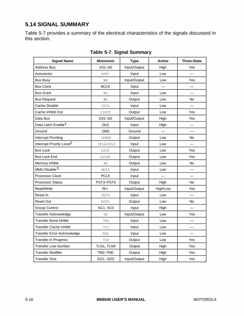
5-16 M68040 USER’S MANUAL MOTOROLA
5.14 SIGNAL SUMMARY
Table 5-7 provides a summary of the electrical characteristics of the signals discussed inthis section.
Table 5-7. Signal Summary
Signal Name Mnemonic Type Active Three-State
Address Bus A31–A0 Input/Output High Yes
Autovector AVEC Input Low —
Bus Busy BB Input/Output Low Yes
Bus Clock BCLK Input — —
Bus Grant BG Input Low —
Bus Request BR Output Low No
Cache Disable CDIS Input Low —
Cache Inhibit Out CIOUT Output Low Yes
Data Bus D31–D0 Input/Output High Yes
Data Latch Enable1 DLE Input High —
Ground GND Ground — —
Interrupt Pending IPEND Output Low No
Interrupt Priority Level2 IPL2–IPL0 Input Low —
Bus Lock LOCK Output Low Yes
Bus Lock End LOCKE Output Low Yes
Memory Inhibit MI Output Low No
MMU Disable3 MDIS Input Low —
Processor Clock PCLK Input — —
Processor Status PST3–PST0 Output High No
Read/Write R/W Input/Output High/Low Yes
Reset In RSTI Input Low —
Reset Out RSTO Output Low No
Snoop Control SC1, SC0 Input High —
Transfer Acknowledge TA Input/Output Low Yes
Transfer Burst Inhibit TBI Input Low —
Transfer Cache Inhibit TCI Input Low —
Transfer Error Acknowledge TEA Input Low —
Transfer in Progress TIP Output Low Yes
Transfer Line Number TLN1, TLN0 Output High Yes
Transfer Modifier TM2–TM0 Output High Yes
Transfer Size SIZ1, SIZ0 Input/Output High Yes
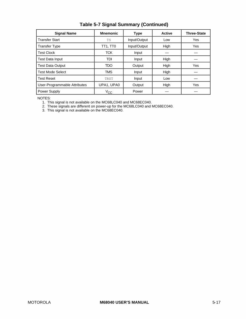
MOTOROLA M68040 USER’S MANUAL 5-17
Table 5-7 Signal Summary (Continued)
Signal Name Mnemonic Type Active Three-State
Transfer Start TS Input/Output Low Yes
Transfer Type TT1, TT0 Input/Output High Yes
Test Clock TCK Input — —
Test Data Input TDI Input High —
Test Data Output TDO Output High Yes
Test Mode Select TMS Input High —
Test Reset TRST Input Low —
User-Programmable Attributes UPA1, UPA0 Output High Yes
Power Supply VCC Power — —
NOTES:1. This signal is not available on the MC68LC040 and MC68EC040.2. These signals are different on power-up for the MC68LC040 and MC68EC040.3. This signal is not available on the MC68EC040.

5-18 M68040 USER’S MANUAL MOTOROLA
MOTOROLA M68040 USER’S MANUAL 6-1
SECTION 6IEEE 1149.1A TEST ACCESS PORT (JTAG)
NOTE
This section does not apply to the MC68040V andMC68EC040V. Refer to Appendix C MC68040V andMC68EC040 for details. All references to M68040 in thissection only, refer to the MC68040, MC68LC040, andMC68EC040.
The M68040 includes dedicated user-accessible test logic that is fully compatible with theIEEE standard 1149.1A Standard Test Access Port and Boundary Scan Architecture.Problems associated with testing high-density circuit boards have led to the standard’sdevelopment under the sponsorship of the IEEE Test Technology Committee and theJoint Test Action Group (JTAG).
This section is to be used in conjunction with the supporting IEEE document and includesthose chip-specific items that the IEEE standard requires to be defined and additionalinformation specific to the M68040 implementation. For example, the IEEE standard1149.1A test access port (TAP) controller states are referenced in this section but are notdescribed. For these details and application information regarding the standard, refer tothe IEEE standard 1149.1A document.
The M68040 implementation supports circuit board test strategies based on the standard.The test logic utilizes static logic design and is system logic independent of the device.The M68040 implementation provides capabilities to:
a. Perform boundary scan operations to test circuit board electrical continuity,
b. Bypass the M68040 by reducing the shift register path to a single cell,
c. Sample the M68040 system pins during operation and transparently shift out theresult,
d. Disable the output drive to output-only pins during circuit board testing, and
e. Select one of two output drivers on a pin-by-pin basis.
NOTE
The IEEE standard 1149.1A test logic cannot be consideredcompletely benign to those planning not to use this capability.Certain precautions must be observed to ensure that this logicdoes not interfere with system operation. Refer to 6.5Disabling the IEEE Standard 1149.1A Operation.

6-2 M68040 USER’S MANUAL MOTOROLA
6.1 OVERVIEW
Figure 6-1 illustrates a block diagram of the M68040 implementation of IEEE standard1149.1A. The test logic includes a 16-state dedicated TAP controller. These 16 controllerstates are defined in detail in the IEEE standard 1149.1A, but only 8 are included in thissection.
Test-Logic-Reset Run-Test/IdleCapture-IR Capture-DRUpdate-IR Update-DRShift-IR Shift-DR
The TAP controller provides access to five dedicated signal pins:
TCK—A test clock input that synchronizes the test logic.
TMS—A test mode select input with an internal pullup resistor sampled on the rising edge of TCK to sequence the TAP controller.
TDI—A test data input with an internal pullup resistor sampled on the rising edge of TCK.
TDO—A three-state test data output actively driven only in the shift-IR and shift-DR controller states that changes on the falling edge of TCK.
TRST—An active-low asynchronous reset with an internal pullup resistor that forces the TAP controller into the test-logic-reset state.
The test logic also includes an instruction shift register and two test data registers, aboundary scan register and a bypass register. The boundary scan register links all devicesignal pins into the instruction shift register.
TDI
TDO
TMS
TCK
TRST
3-BIT INSTRUCTION SHIFT REGISTER
LATCHED DECODER
184-BIT BOUNDARY SCAN REGISTER
TEST DATA REGISTERS
BYPASS
MU
X
TAP
CO
NTR
OLL
ER
MU
X
183 0
02
Figure 6-1. M68040 Test Logic Block Diagram

MOTOROLA M68040 USER’S MANUAL 6-3
6.2 INSTRUCTION SHIFT REGISTER
The M68040 IEEE standard 1149.1A implementation includes a 3-bit instruction shiftregister without parity. The register shifts one of eight instructions, which can either selectthe test to be performed or access a test data register, or both. Data is transferred fromthe instruction shift register to latched decoded outputs during the update-IR state. Theinstruction shift register is reset to all ones in the TAP controller test-logic-reset state,which is equivalent to selecting the BYPASS instruction. During the capture-IR state, thebinary value 001 is loaded into the parallel inputs of the instruction shift register.
The M68040 IEEE standard 1149.1A implementation includes three mandatory publicinstructions (BYPASS, SAMPLE/PRELOAD, and EXTEST) and four manufacturer's publicinstructions. The four manufacturer’s public instructions provide the capability to disable alldevice output drivers, operate the device in a BYPASS configuration without a systemclocking requirement, and select one of two output drive capabilities on a pin-by-pin basis.The M68040 implementation does not support the optional standard public instructions.Table 6-1 lists the three bits used in the instruction shift register to decode the instructionsand their related encodings. Note that the least significant bit of the instruction (bit 0) is thefirst bit to be shifted into the instruction shift register.
Table 6-1. IEEE Standard 1149.1A Instructions
Bit 2 Bit 1 Bit 0 Instruction Selected Test Data Register Accessed
0 0 0 EXTEST Boundary Scan
0 0 1 HIGHZ Bypass
0 1 0 SAMPLE/PRELOAD Boundary Scan
0 1 1 DRVCTL.T Boundary Scan
1 0 0 SHUTDOWN Bypass
1 0 1 PRIVATE Bypass
1 1 0 DRVCTL.S Boundary Scan
1 1 1 BYPASS Bypass
EXTEST, HIGHZ, DRVCTL.T, SHUTDOWN, and PRIVATE have a PCLK and BCLKrestriction. Failure to comply with this restriction results in potential internal damage to thedevice (see 6.4 Restrictions). Once the restriction is complied with, SHUTDOWN,EXTEST, HIGHZ, and DRVCTL.T can be entered regardless of order. The system clocks(PCLK and BCLK) must be kept running while in the SAMPLE/PRELOAD, DRVCLT.S,and BYPASS instructions. Failure to do so could result in potential internal damage to thedevice.
6.2.1 EXTEST
The external test instruction (EXTEST) selects the 184-bit boundary scan register. Thisinstruction also activates two internal functions that are intended to protect the device frompotential damage while performing boundary scan operations.
6-4 M68040 USER’S MANUAL MOTOROLA
EXTEST asserts internal reset for the M68040 system logic to force a predictable benigninternal state and activates an internal keep-alive clock to protect the device from potentialinternal damage. This internal clock eliminates the requirement to keep the system clocks(PCLK and BCLK) running during EXTEST operations and allows these two system clockpins to be included in boundary scan testing.
6.2.2 HIGHZ
The HIGHZ instruction is an optional instruction provided as a Motorola public instructionto anticipate the need to backdrive output pins during circuit board testing. The HIGHZinstruction activates an internal keep-alive clock, asserts internal system reset, selects thebypass register, and forces all output and bidirectional pins to the high-impedance state.
Asserting TRST or holding TMS high and clocking TCK for at least five rising edgescauses the TAP controller to enter the test-logic-reset state. Using only the TMS and TCKpins and the capture-IR and update-IR states invokes the HIGHZ instruction. This schemeworks because the value captured by the instruction shift register during the capture-IRstate is identical to the HIGHZ opcode.
6.2.3 SAMPLE/PRELOAD
The SAMPLE/PRELOAD instruction provides two separate functions. First, it provides ameans to obtain a sample system data and control signal. Sampling occurs on the risingedge of TCK in the capture-DR state. The user can observe the data by shifting it throughthe boundary scan register to output TDO using the shift-DR state. Both the data captureand the shift operations are transparent to system operation. The user must provide someform of external synchronization to achieve meaningful results since there is no internalsynchronization between TCK and BCLK.
The second function of the SAMPLE/PRELOAD instruction is to initialize the boundaryscan register output cells before selecting EXTEST, which is accomplished by ignoringdata being shifted out of TDO while shifting in initialization data. The update-DR state canthen be used to initialize the boundary scan register and ensure that known data andoutput state will occur on the outputs after entering the EXTEST instruction.
6.2.4 DRVCTL.T
The DRVCTL.T instruction is a Motorola public instruction that provides the ability to selectone of two output drivers on a pin-by-pin basis. It is intended for use with EXTEST orSHUTDOWN to provide an IEEE-compatible environment to select the output drivers forboard-level test environments. This instruction allows data in the boundary scan register toselect the output driver. A logic zero in the appropriate boundary scan output cell (seeTable 6-1) selects the large buffer, and a logic one selects the small buffer (see Section 7Bus Operation). Data captured in the capture-DR state for this instruction is identical tothat captured during EXTEST: output data cells for outputs and pin state for inputs. Notethat no data relevant to the drive control function is captured during the capture-DR state.
MOTOROLA M68040 USER’S MANUAL 6-5
The DRVCTL.T instruction is intended to be used in test applications in conjunction withthe EXTEST and SHUTDOWN instructions and not for system applications. It thereforediffers from DRVCTL.S in that this instruction invokes the keep-alive clock, asserts theinternal reset, and the test logic, not the system logic, has control of the I/O pins.
When the system logic has control of signal pin I/O directions and levels, the drive controllatch is loaded from the IPL2–IPL0 pins during the negation of RSTI. DRVCTL.T overwritesthis value with boundary scan data in the update-DR state. The selected output driverstate remains unchanged if only the DRVCTL.T, EXTEST, or SHUTDOWN instructionsare invoked. If an instruction other than one of these three is executed, the system logicprotocol regains control of the output driver state and overwrites the value that theDRVCTL.T instruction previously defined.
Note that the output drive control state does not change while the 1149.1A instruction isone of the three instructions DRVCTL.T, EXTEST, or SHUTDOWN. If DRVCTL.T changesthe output driver state and then the test-logic-reset state is entered, the instruction shiftregister is reset to BYPASS, and the system logic can change the output driver state.
6.2.5 SHUTDOWN
This instruction provides an opcode for automatic test pattern generation (ATPG)programs to cope with the clocking protocol required to stop the system clocks. Thisinstruction asserts internal system reset, activates an internal keep alive clock, and selectsthe bypass register. Internal decoding of the instruction selects the bypass register, andthe test logic, not the system logic, has control of the I/O ports. Note that initializing theboundary scan data register and then selecting the SHUTDOWN instruction provides aclamping function. The test logic controls the I/O state, and the bypass register isselected.
6.2.6 PRIVATE
Motorola reserves this instruction for manufacturing use. The instruction does not changepin I/O as defined for system operation.
6.2.7 DRVCTL.S
The DRVCTL.S instruction controls the output driver selection on a pin-by-pin basis. Thisinstruction allows data in the boundary scan register to select the output driver during theupdate-DR state when the system logic has control of the signal I/O directions and levels.A logic zero selects the large buffer or driver; a logic one selects the small buffer or driver(see Table 6-1).
The DRVCTL.S instruction is intended to be used in system applications and not in testapplications. In system applications, the system logic has control of the signal pin I/Odirections and levels; whereas, in test applications, the 1149.1A test logic has control of it.It therefore differs from DRVCTL.T in that this instruction does not invoke the internal keepalive clock, it does not assert the internal reset, and the system logic, not the test logic,
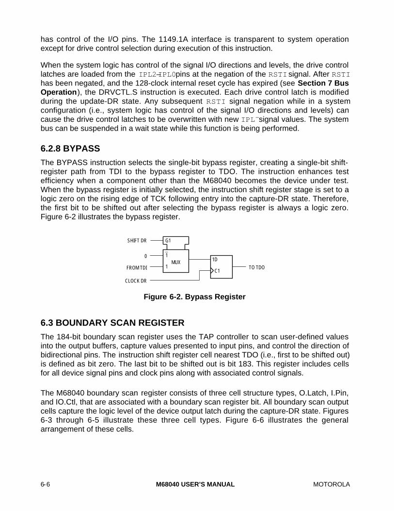
6-6 M68040 USER’S MANUAL MOTOROLA
has control of the I/O pins. The 1149.1A interface is transparent to system operationexcept for drive control selection during execution of this instruction.
When the system logic has control of the signal I/O directions and levels, the drive controllatches are loaded from the IPL2–IPL0 pins at the negation of the RSTI signal. After RSTIhas been negated, and the 128-clock internal reset cycle has expired (see Section 7 BusOperation), the DRVCTL.S instruction is executed. Each drive control latch is modifiedduring the update-DR state. Any subsequent RSTI signal negation while in a systemconfiguration (i.e., system logic has control of the signal I/O directions and levels) cancause the drive control latches to be overwritten with new IPL signal values. The systembus can be suspended in a wait state while this function is being performed.
6.2.8 BYPASS
The BYPASS instruction selects the single-bit bypass register, creating a single-bit shift-register path from TDI to the bypass register to TDO. The instruction enhances testefficiency when a component other than the M68040 becomes the device under test.When the bypass register is initially selected, the instruction shift register stage is set to alogic zero on the rising edge of TCK following entry into the capture-DR state. Therefore,the first bit to be shifted out after selecting the bypass register is always a logic zero.Figure 6-2 illustrates the bypass register.
1MUX
1
G1
1D
C1
CLOCK DR
FROM TDI
0
SHIFT DR
TO TDO
Figure 6-2. Bypass Register
6.3 BOUNDARY SCAN REGISTER
The 184-bit boundary scan register uses the TAP controller to scan user-defined valuesinto the output buffers, capture values presented to input pins, and control the direction ofbidirectional pins. The instruction shift register cell nearest TDO (i.e., first to be shifted out)is defined as bit zero. The last bit to be shifted out is bit 183. This register includes cellsfor all device signal pins and clock pins along with associated control signals.
The M68040 boundary scan register consists of three cell structure types, O.Latch, I.Pin,and IO.Ctl, that are associated with a boundary scan register bit. All boundary scan outputcells capture the logic level of the device output latch during the capture-DR state. Figures6-3 through 6-5 illustrate these three cell types. Figure 6-6 illustrates the generalarrangement of these cells.
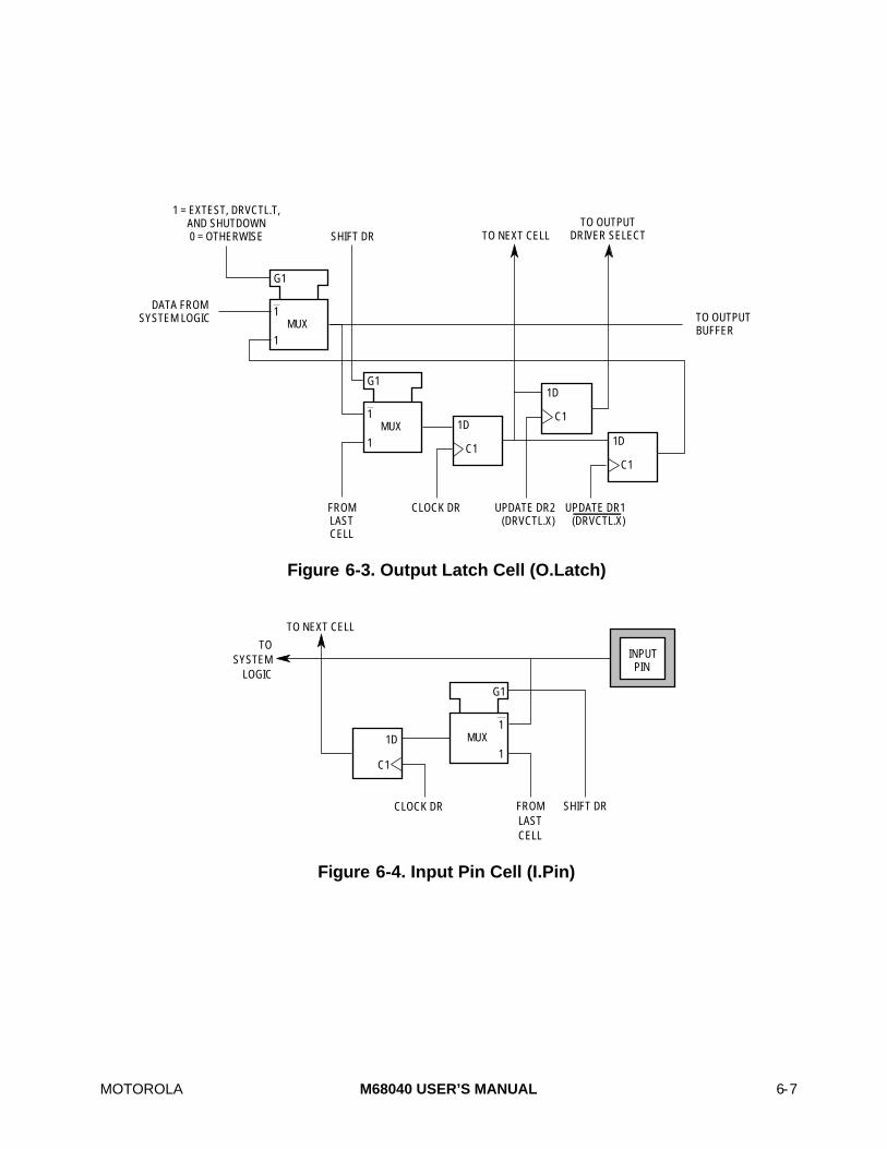
MOTOROLA M68040 USER’S MANUAL 6-7
DATA FROM SYSTEM LOGIC
FROM LAST CELL
CLOCK DR UPDATE DR2 (DRVCTL.X)
SHIFT DR TO NEXT CELL
TO OUTPUT BUFFER
1 = EXTEST, DRVCTL.T, AND SHUTDOWN 0 = OTHERWISE
1MUX
1
G1
1D
C1
UPDATE DR1 (DRVCTL.X)
TO OUTPUT DRIVER SELECT
1D
C11D
C11MUX
1
G1
Figure 6-3. Output Latch Cell (O.Latch)
FROM LAST CELL
TO SYSTEM
LOGIC
SHIFT DRCLOCK DR
TO NEXT CELL
1D
C11
MUX1
G1
INPUT PIN
Figure 6-4. Input Pin Cell (I.Pin)

6-8 M68040 USER’S MANUAL MOTOROLA
OUTPUT CONTROL FROM SYSTEM LOGIC
FROM LAST CELL
CLOCK DR
SHIFT DR TO NEXT CELL
TO OUTPUT BUFFER (1 = DRIVE)
1 = EXTEST 0 = OTHERWISE
1D
C1
1MUX
1
G1
1MUX
1
G1
UPDATE DR
1D
C1
R
RESET
Figure 6-5. Output Control Cells (IO.Ctl)
FROM LAST CELL
OUTPUT DATA
INPUT DATA
OUTPUT ENABLE
TO NEXT CELL
TO NEXT PIN PAIR
I/O.CTL
O.LATCH
I.PIN
EN INPUT PIN
Figure 6-6. General Arrangement of Bidirectional Pins

MOTOROLA M68040 USER’S MANUAL 6-9
All M68040 bidirectional pins include two boundary scan data cells, an input, and anoutput. One of five associated boundary scan control cells controls each bidirectional pin.If these cells contain a logic one, the associated bidirectional or three-state pin will beconfigured as an output and enabled. The cell captures the current value during thecapture-DR state. All five control cells are reset (i.e., logic zero) in the test-logic-resetstate. The five bidirectional/three-state control cells and their boundary scan register bitpositions are as follows:
Cell Name Bit
io.ab 150
io.db 151
io.2 154
io.1 155
io.0 156
Table 6-2 lists the 184 boundary scan bit definitions. The first column in the table definesthe bit position in the boundary scan register. The second column references one of thethree cell types. The third column lists the pin name for all pin-related cells. The fourthcolumn lists the system pin type for convenience where TS-Output indicates a three-stateoutput pin and I/O indicates a bidirectional pin. The last column lists the name of theassociated control bit of the boundary scan register for three-state output and bidirectionalpins. The boundary scan description language (BSDL) type for each cell can be found innote 1.

6-10 M68040 USER’S MANUAL MOTOROLA
Table 6-2. Boundary Scan Bit Definitions1
Bit Cell TypePin/CellName Pin Type
OutputCtrl Cell
0 O.Latch RSTO Output2 (Note 3)
1 O.Latch IPEND Output2 (Note 3)
2 O.Latch CIOUT TS-Output2 io.0
3 O.Latch UPA0 TS-Output2 io.0
4 O.Latch UPA1 TS-Output2 io.0
5 O.Latch TT0 I/O2 io.0
6 I.Pin TT0 I/O io.0
7 O.Latch TT1 I/O2 io.0
8 I.Pin TT1 I/O io.0
9 O.Latch A10 I/O2 io.ab
10 I.Pin A10 I/O io.ab
11 O.Latch A11 I/O2 io.ab
12 I.Pin A11 I/O io.ab
13 O.Latch A12 I/O2 io.ab
14 I.Pin A12 I/O io.ab
15 O.Latch A13 I/O2 io.ab
16 I.Pin A13 I/O io.ab
17 O.Latch A14 I/O2 io.ab
18 I.Pin A14 I/O io.ab
19 O.Latch A15 I/O2 io.ab
20 I.Pin A15 I/O io.ab
21 O.Latch A16 I/O2 io.ab
22 I.Pin A16 I/O io.ab
23 O.Latch A17 I/O2 io.ab
24 I.Pin A17 I/O io.ab
25 O.Latch A18 I/O2 io.ab
26 I.Pin A18 I/O io.ab
27 O.Latch A19 I/O2 io.ab
28 I.Pin A19 I/O io.ab
29 O.Latch A20 I/O2 io.ab
30 I.Pin A20 I/O io.ab
31 O.Latch A21 I/O2 io.ab
32 I.Pin A21 I/O io.ab
33 O.Latch A22 I/O2 io.ab
34 I.Pin A22 I/O io.ab
35 O.Latch A23 I/O2 io.ab
36 I.Pin A23 I/O io.ab
Bit Cell TypePin/CellName Pin Type
OutputCtrl Cell
37 O.Latch A24 I/O2 io.ab
38 I.Pin A24 I/O io.ab
39 O.Latch A25 I/O2 io.ab
40 I.Pin A25 I/O io.ab
41 O.Latch A26 I/O2 io.ab
42 I.Pin A26 I/O io.ab
43 O.Latch A27 I/O2 io.ab
44 I.Pin A27 I/O io.ab
45 O.Latch A28 I/O2 io.ab
46 I.Pin A28 I/O io.ab
47 O.Latch A29 I/O2 io.ab
48 I.Pin A29 I/O io.ab
49 O.Latch A30 I/O2 io.ab
50 I.Pin A30 I/O io.ab
51 O.Latch A31 I/O2 io.ab
52 I.Pin A31 I/O io.ab
53 O.Latch D0 I/O2 io.db
54 O.Latch D1 I/O2 io.db
55 O.Latch D2 I/O2 io.db
56 O.Latch D3 I/O2 io.db
57 O.Latch D4 I/O2 io.db
58 O.Latch D5 I/O2 io.db
59 O.Latch D6 I/O2 io.db
60 O.Latch D7 I/O2 io.db
61 O.Latch D8 I/O2 io.db
62 O.Latch D9 I/O2 io.db
63 O.Latch D10 I/O2 io.db
64 O.Latch D11 I/O2 io.db
65 O.Latch D12 I/O2 io.db
66 O.Latch D13 I/O2 io.db
67 O.Latch D14 I/O2 io.db
68 O.Latch D15 I/O2 io.db
69 O.Latch D16 I/O2 io.db
70 O.Latch D17 I/O2 io.db
71 O.Latch D18 I/O2 io.db
72 O.Latch D19 I/O2 io.db
73 O.Latch D20 I/O2 io.db

MOTOROLA M68040 USER’S MANUAL 6-11
Table 6-2. Boundary Scan Bit Definitions (Continued)
Bit Cell TypePin/CellName Pin Type
OutputCtrl Cell
74 O.Latch D21 I/O2 io.db
75 O.Latch D22 I/O2 io.db
76 O.Latch D23 I/O2 io.db
77 O.Latch D24 I/O2 io.db
78 O.Latch D25 I/O2 io.db
79 O.Latch D26 I/O2 io.db
80 O.Latch D27 I/O2 io.db
81 O.Latch D28 I/O2 io.db
82 O.Latch D29 I/O2 io.db
83 O.Latch D30 I/O2 io.db
84 O.Latch D31 I/O2 io.db
85 I.Pin D0 I/O io.db
86 I.Pin D1 I/O io.db
87 I.Pin D2 I/O io.db
88 I.Pin D3 I/O io.db
89 I.Pin D4 I/O io.db
90 I.Pin D5 I/O io.db
91 I.Pin D6 I/O io.db
92 I.Pin D7 I/O io.db
93 I.Pin D8 I/O io.db
94 I.Pin D9 I/O io.db
95 I.Pin D10 I/O io.db
96 I.Pin D11 I/O io.db
97 I.Pin D12 I/O io.db
98 I.Pin D13 I/O io.db
99 I.Pin D14 I/O io.db
100 I.Pin D15 I/O io.db
101 I.Pin D16 I/O io.db
102 I.Pin D17 I/O io.db
103 I.Pin D18 I/O io.db
104 I.Pin D19 I/O io.db
105 I.Pin D20 I/O io.db
106 I.Pin D21 I/O io.db
107 I.Pin D22 I/O io.db
108 I.Pin D23 I/O io.db
109 I.Pin D24 I/O io.db
110 I.Pin D25 I/O io.db
Bit Cell TypePin/CellName Pin Type
OutputCtrl Cell
111 I.Pin D26 I/O io.db
112 I.Pin D27 I/O io.db
113 I.Pin D28 I/O io.db
114 I.Pin D29 I/O io.db
115 I.Pin D30 I/O io.db
116 I.Pin D31 I/O io.db
117 O.Latch A9 I/O2 io.ab
118 I.Pin A9 I/O io.ab
119 O.Latch A8 I/O2 io.ab
120 I.Pin A8 I/O io.ab
121 O.Latch A7 I/O2 io.ab
122 I.Pin A7 I/O io.ab
123 O.Latch A6 I/O2 io.ab
124 I.Pin A6 I/O io.ab
125 O.Latch A5 I/O2 io.ab
126 I.Pin A5 I/O io.ab
127 O.Latch A4 I/O2 io.ab
128 I.Pin A4 I/O io.ab
129 O.Latch A3 I/O2 io.ab
130 I.Pin A3 I/O io.ab
131 O.Latch A2 I/O2 io.ab
132 I.Pin A2 I/O io.ab
133 O.Latch A1 I/O2 io.ab
134 I.Pin A1 I/O io.ab
135 O.Latch A0 I/O2 io.ab
136 I.Pin A0 I/O io.ab
137 O.Latch TM2 TS-Output2 io.0
138 O.Latch TM1 TS-Output2 io.0
139 O.Latch TM0 TS-Output2 io.0
140 O.Latch TLN1 TS-Output2 io.0
141 O.Latch TLN0 TS-Output2 io.0
142 O.Latch SIZ0 I/O2 io.0
143 I.Pin SIZ0 I/O io.0
144 O.Latch R/W I/O2 io.0
145 I.Pin R/W I/O io.0
146 O.Latch LOCKE TS-Output2 io.1
147 O.Latch SIZ1 I/O2 io.0

6-12 M68040 USER’S MANUAL MOTOROLA
Table 6-2. Boundary Scan Bit Definitions (Concluded)
Bit Cell TypePin/CellName Pin Type
OutputCtrl Cell
148 I.Pin SIZ1 I/O io.0
149 O.Latch LOCK TS-Output2 io.1
150 IO.Ctl io.ab — (Note 4)
151 IO.Ctl io.db — (Note 4)
152 O.Latch MI Output2 (Note 3)
153 O.Latch BR Output2 (Note 3)
154 IO.Ctl io.2 — (Note 4)
155 IO.Ctl io.1 — (Note 4)
156 IO.Ctl io.0 — (Note 4)
157 O.Latch TS I/O2 io.0
158 I.Pin TS I/O io.0
159 O.Latch BB I/O2 io.1
160 I.Pin BB I/O io.1
161 O.Latch TIP TS-Output2 io.1
162 O.Latch PST3 Output2 (Note 3)
163 O.Latch PST2 Output2 (Note 3)
164 O.Latch PST1 Output2 (Note 3)
165 O.Latch PST0 Output2 (Note 3)
Bit Cell TypePin/CellName Pin Type
OutputCtrl Cell
166 O.Latch TA I/O2 io.2
167 I.Pin TA I/O io.2
168 I.Pin TEA Input —
169 I.Pin BG Input —
170 I.Pin SC1 Input —
171 I.Pin SC0 Input —
172 I.Pin TBI Input —
173 I.Pin AVEC Input —
174 I.Pin TCI Input —
175 I.Pin DLE5 Input —
176 I.Pin PCLK Input —
177 I.Pin BCLK Input —
178 I.Pin IPL0 Input —
179 I.Pin IPL1 Input —
180 I.Pin IPL2 Input —
181 I.Pin RSTI Input —
182 I.Pin CDIS Input —
183 I.Pin MDIS6 Input —
NOTES:1. I.Pin, IO.Ctl, and O.Latch are equivalent to the BSDL descriptions: BC_4, BC_2, and BC_2, respectively.2. Boundary scan register bit positions that are used during the drive control (DRVCTL.X) instructions.3. These output-only cells can be turned off (high impedance) by using the HIGHZ instruction.4. All of the control signals (IO.Ctl) are cleared in the test-logic-reset state.5. Renamed JS0 on the MC68LC040 and MC68EC040.6. Renamed JS1 on the MC68EC040.
6.4 RESTRICTIONS
The test logic is implemented using static logic design, and TCK can be stopped in eithera high or low state without loss of data. The system logic, however, includes considerabledynamic logic. For this reason, the system clocks (PCLK and BCLK) cannot be stopped orallowed to run slower than the specified frequency except when the EXTEST, HIGHZ,DRVCTL.T, or SHUTDOWN instructions have been properly invoked.
PCLK and BCLK must be kept running for two additional BCLK periods upon initial entryinto any of the four instructions, EXTEST, HIGHZ, DRVCTL.T, or SHUTDOWN. Thisrestriction is necessary to allow time for an internal reset to propagate through an internalsynchronizer. After this period, the user has complete time-domain freedom with the twosystem clock pins. After any of the four instructions has been properly entered, theseinstructions can be executed in any order without a time-domain clocking restriction.Entering any instruction other than one of these four requires that the system clocks be

MOTOROLA M68040 USER’S MANUAL 6-13
restarted, and a proper reentry into any of the four instructions is again required before thesystem clocks can be stopped.
Control over the output enable signals using the boundary scan register and the EXTESTand HIGHZ instructions requires a compatible circuit-board test environment to avoiddestructive configurations. The user is responsible for avoiding situations in which theM68040 output drivers are enabled into actively driven networks.
The TRST signal provides the ability for an asynchronous reset of the test logic andrequires no internal clocking to force the TAP controller into the test-logic-reset state. Thissignal should be asserted during system power-up to initialize the 1149.1A test interfaceand avoid the potential for board-level bus conflicts. Essentially the TRST signal providesthe ability to prevent possible board-level bus contention during power-up due to the testlogic having control of the pins. The device has no internal power-up reset circuit. TheTRST signal should be treated similar to the RSTI signal for board design considerationsconcerning power-up conditions.
Negation of the TRST signal requires certain precautions to achieve a predictable TAPcontroller state. The TMS signal is sampled on the rising edge of TCK and sequences theTAP controller. If TMS is low and TRST is negated simultaneously with the rising edge ofTCK, the resultant TAP controller state is unpredictable but will be either test-logic-reset orrun-test/idle. To avoid this uncertainty, either 1) the negation of TRST can be synchronizedwith the falling edge of TCK or 2) TMS can remain high until after TRST negation.Alternatively, holding TMS low for two or more TCK periods following TRST negationensures that the TAP controller is in the run-test/idle state.
6.5 DISABLING THE IEEE STANDARD 1149.1A OPERATION
There are two considerations for non-IEEE standard 1149.1A operation. First, TCK doesnot include an internal pullup resistor and should not be left unconnected to preclude mid-level inputs. The second consideration is to ensure that the IEEE standard 1149.1A testlogic remains transparent to the system logic by providing the ability to force the test-logic-reset state.
Figure 6-7 illustrates disabling the IEEE standard 1149.1A operation through connectingTRST directly or through a resistor to ground or a suitable logic network. Connecting TRSTto RSTI while TCK is held either high or low meets the two considerations. If a pulseasserts TRST , the TAP controller is forced into the test-logic-reset state and can remain inthis state as long as a rising edge on the TCK signal does not occur when TMS is low.

6-14 M68040 USER’S MANUAL MOTOROLA
TDI
TMS
TRST
TCLK
TD0 NO CONNECTION
+5V
1K
Figure 6-7. Circuit DisablingIEEE Standard 1149.1A

MOTOROLA M68040 USER’S MANUAL 6-15
6.6 MOTOROLA M68040 BSDL DESCRIPTION (VERSION 2.2)
Revision List:1. LOCK and LOCKE controlled by io.1 vice io.0 (4D98D).
3. No other changes to Version 2.1 BSDL.
2. Instruction opcodes changed for SAMPLE, SHUTDOWN, and BYPASS.
3. New instructions DRVCTL.T, DRVCTL.S and PRIVATE added.
4. New instructions DRVCTL.T and DRVCTL.S renamed to DRVCTL_T andDRVCTL_S for syntax compatibility.
5. Register access specified for DRVCTL_T, DRVCTL_S, and PRIVATE instructions.
6. No other changes to Version 1.0 BSDL.
Package Type: 18 x 18 PGA
This BSDL is for the newer MC68040 mask sets of E26A and after (roughly after thesecond half of 1992). It does not include the 0.8-µm mask sets D43B, D50D, and D98D.For MC68LC040 and MC68EC040, two pin names have changed. To make the necessarymodifications, change all occurrences of DLE to JS0 and MDIS to JS1.
entity MC68040 is
generic(PHYSICAL_PIN_MAP:string := "PGA_18x18");
port (TDI: in bit;TDO: out bit;TMS: in bit;TCK: in bit;TRST: in bit;RSTO: buffer bit;IPEND: buffer bit;CIOUT: out bit;UPA: out bit_vector(0 to 1);TT: inout bit_vector(0 to 1);A: inout bit_vector(0 to 31);D: inout bit_vector(0 to 31);LOCKE: out bit;LOCK: out bit;R_W: inout bit;TLN: out bit_vector(0 to 1);TM: out bit_vector(0 to 2);SIZ: inout bit_vector(0 to 1);MI: buffer bit;BR: buffer bit;TS: inout bit;BB: inout bit;TIP: out bit;PST: buffer bit_vector(0 to 3);TA: inout bit;TEA: in bit;BG: in bit;SC: in bit_vector(0 to 1);TBI: in bit;AVEC: in bit;TCI: in bit;

6-16 M68040 USER’S MANUAL MOTOROLA
DLE: in bit;PCLK: in bit;BCLK: in bit;IPL: in bit_vector(0 to 2);RSTI: in bit;CDIS: in bit;MDIS: in bit;EGND: linkage bit_vector(1 to 23);EVDD: linkage bit_vector(1 to 12);IGND: linkage bit_vector(1 to 12);IVDD: linkage bit_vector(1 to 7);CGND: linkage bit_vector(1 to 2);CVDD: linkage bit_vector(1 to 6);PGND: linkage bit_vector(1 to 3);PVDD: linkage bit_vector(1 to 2));
use STD_1149_1_1990.all;attribute PIN_MAP of MC68040 : entity is PHYSICAL_PIN_MAP;
—18x18 PGA Pin Map
constant PGA_18x18 : PIN_MAP_STRING :="TDI: S3, " &"TDO: T2, " &"TMS: S5, " &"TCK: S4, " &"TRST: T3, " &"RSTO: R3, " &"IPEND: S1, " &"CIOUT: R1, " &"UPA: (Q3, Q1), " &"TT: (P3, P2), " &"A: (L18, K18, J17, J18, H18, G18, G16, F18, E18, F16, P1, N3, " &" N1, M1, L1, K1, K2, J1, H1, J2, G1, F1, E1, G3, " &" D1, F3, E2, C1, E3, B1, D3, A1), " &"D: (C3, B3, C4, A2, A3, A4, A5, A6, B7, A7, A8, A9, " &" A10, A11, A12, A13, B11, A14, B12, A15, A16, A17, B16, C15, " &" A18, C16, B18, D16, C18, E16, E17, D18), " &"LOCKE: R18, " &"LOCK: S18, " &"R_W: N16, " &"TLN: (Q18, P18), " &"TM: (N18, M18, K17), " &"SIZ: (P17, P16), " &"MI: Q16, " &"BR: T18, " &"TS: R16, " &"BB: T17, " &"TIP: R15, " &"PST: (T15, S14, R14, T16), " &"TA: T14, " &"TEA: S13, " &"BG: T13, " &"SC: (T12, S12), " &"TBI: S11, " &"AVEC: T11, " &
MOTOROLA M68040 USER’S MANUAL 6-17
"TCI: T10, " &"DLE: T9, " &"PCLK: R9, " &"BCLK: R7, " &"IPL: (T8, T7, T6), " &"RSTI: S7, " &"CDIS: T5, " &"MDIS: S6, " &"EGND: (S2, Q2, N2, L2, H2, F2, D2, B2, B4, B6, B8, B10, " &" B13, B15, B17, D17, F17, H17, L17, N17, Q17, S17, S15), " &"EVDD: (R2, M2, G2, C2, B5, B9, B14, C17, G17, M17, R17, S16), " &"IGND: (T4, R4, L3, K3, C7, C9, C11, K16, M16, R13, R11, S10), " &"IVDD: (R5, M3, C8, C10, C12, L16, R12), " &"CGND: (C6, C13), " &"CVDD: (J3, H3, C5, C14, H16, J16), " &"PGND: (S9, R10, R6), " &"PVDD: (S8, R8) " ;
—Other Pin Maps here when documented
attribute TAP_SCAN_IN of TDI:signal is true;attribute TAP_SCAN_OUT of TDO:signal is true;attribute TAP_SCAN_MODE of TMS:signal is true;attribute TAP_SCAN_CLOCK of TCK:signal is (10.0e6, BOTH);attribute TAP_SCAN_RESET of TRST:signal is true;attribute INSTRUCTION_LENGTH of MC68040:entity is 3;attribute INSTRUCTION_OPCODE of MC68040:entity is
"EXTEST (000), " &"HI_Z (001), " &"SAMPLE (010), " &"DRVCTL.T (011), " &"SHUTDOWN (100), " &"PRIVATE (101), " &"DRVCTL.S (110), " &"BYPASS (111) " ;
attribute INSTRUCTION_CAPTURE of MC68040:entity is "001";attribute INSTRUCTION_DISABLE of MC68040:entity is "HI_Z";attribute REGISTER_ACCESS of MC68040:entity is
"BYPASS (SHUTDOWN, HI_Z, PRIVATE), " &"BOUNDARY (DRVCTL_T, DRVCTL_S) " ;
attribute BOUNDARY_CELLS of MC68040:entity is
"BC_2, BC_4 " ;
attribute BOUNDARY_LENGTH of MC68040:entity is 184;attribute BOUNDARY_REGISTER of MC68040:entity is

6-18 M68040 USER’S MANUAL MOTOROLA
num cell port function safe ccell dsval rslt
"0 (BC_2, RSTO, output2, X), " &"1 (BC_2, IPEND, output2, X), " &"2 (BC_2, CIOUT, output3, X, 156, 0, Z), " & —156 = io.0"3 (BC_2, UPA(0), output3, X, 156, 0, Z), " &"4 (BC_2, UPA(1), output3, X, 156, 0, Z), " &"5 (BC_2, TT(0), output3, X, 156, 0, Z), " &"6 (BC_4, TT(0), input, X), " &"7 (BC_2, TT(1), output3, X, 156, 0, Z), " &"8 (BC_4, TT(1), input, X), " &"9 (BC_2, A(10), output3, X, 150, 0, Z), " & —150 = io.ab"10 (BC_4, A(10), input, X), " &"11 (BC_2, A(11), output3, X, 150, 0, Z), " &"12 (BC_4, A(11), input, X), " &"13 (BC_2, A(12), output3, X, 150, 0, Z), " &"14 (BC_4, A(12), input, X), " &"15 (BC_2, A(13), output3, X, 150, 0, Z), " &"16 (BC_4, A(13), input, X), " &"17 (BC_2, A(14), output3, X, 150, 0, Z), " &"18 (BC_4, A(14), input, X), " &"19 (BC_2, A(15), output3, X, 150, 0, Z), " &"20 (BC_4, A(15), input, X), " &"21 (BC_2, A(16), output3, X, 150, 0, Z), " &"22 (BC_4, A(16), input, X), " &"23 (BC_2, A(17), output3, X, 150, 0, Z), " &"24 (BC_4, A(17), input, X), " &"25 (BC_2, A(18), output3, X, 150, 0, Z), " &"26 (BC_4, A(18), input, X), " &"27 (BC_2, A(19), output3, X, 150, 0, Z), " &"28 (BC_4, A(19), input, X), " &"29 (BC_2, A(20), output3, X, 150, 0, Z), " &"30 (BC_4, A(20), input, X), " &"31 (BC_2, A(21), output3, X, 150, 0, Z), " &"32 (BC_4, A(21), input, X), " &"33 (BC_2, A(22), output3, X, 150, 0, Z), " &"34 (BC_4, A(22), input, X), " &"35 (BC_2, A(23), output3, X, 150, 0, Z), " &"36 (BC_4, A(23), input, X), " &"37 (BC_2, A(24), output3, X, 150, 0, Z), " &"38 (BC_4, A(24), input, X), " &"39 (BC_2, A(25), output3, X, 150, 0, Z), " &"40 (BC_4, A(25), input, X), " &"41 (BC_2, A(26), output3, X, 150, 0, Z), " &"42 (BC_4, A(26), input, X), " &"43 (BC_2, A(27), output3, X, 150, 0, Z), " &"44 (BC_4, A(27), input, X), " &"45 (BC_2, A(28), output3, X, 150, 0, Z), " &"46 (BC_4, A(28), input, X), " &"47 (BC_2, A(29), output3, X, 150, 0, Z), " &"48 (BC_4, A(29), input, X), " &"49 (BC_2, A(30), output3, X, 150, 0, Z), " &"50 (BC_4, A(30), input, X), " &"51 (BC_2, A(31), output3, X, 150, 0, Z), " &"52 (BC_4, A(31), input, X), " &"53 (BC_2, D(0), output3, X, 151, 0, Z), " & — 151 = io.db"54 (BC_2, D(1), output3, X, 151, 0, Z), " &"55 (BC_2, D(2), output3, X, 151, 0, Z), " &"56 (BC_2, D(3), output3, X, 151, 0, Z), " &

MOTOROLA M68040 USER’S MANUAL 6-19
num cell port function safe ccell dsval rslt
"57 (BC_2, D(4), output3, X, 151, 0, Z), " &"58 (BC_2, D(5), output3, X, 151, 0, Z), " &"59 (BC_2, D(6), output3, X, 151, 0, Z), " &"60 (BC_2, D(7), output3, X, 151, 0, Z), " &"61 (BC_2, D(8), output3, X, 151, 0, Z), " &"62 (BC_2, D(9), output3, X, 151, 0, Z), " &"63 (BC_2, D(10), output3, X, 151, 0, Z), " &"64 (BC_2, D(11), output3, X, 151, 0, Z), " &"65 (BC_2, D(12), output3, X, 151, 0, Z), " &"66 (BC_2, D(13), output3, X, 151, 0, Z), " &"67 (BC_2, D(14), output3, X, 151, 0, Z), " &"68 (BC_2, D(15), output3, X, 151, 0, Z), " &"69 (BC_2, D(16), output3, X, 151, 0, Z), " &"70 (BC_2, D(17), output3, X, 151, 0, Z), " &"71 (BC_2, D(18), output3, X, 151, 0, Z), " &"72 (BC_2, D(19), output3, X, 151, 0, Z), " &"73 (BC_2, D(20), output3, X, 151, 0, Z), " &"74 (BC_2, D(21), output3, X, 151, 0, Z), " &"75 (BC_2, D(22), output3, X, 151, 0, Z), " &"76 (BC_2, D(23), output3, X, 151, 0, Z), " &"77 (BC_2, D(24), output3, X, 151, 0, Z), " &"78 (BC_2, D(25), output3, X, 151, 0, Z), " &"79 (BC_2, D(26), output3, X, 151, 0, Z), " &"80 (BC_2, D(27), output3, X, 151, 0, Z), " &"81 (BC_2, D(28), output3, X, 151, 0, Z), " &"82 (BC_2, D(29), output3, X, 151, 0, Z), " &"83 (BC_2, D(30), output3, X, 151, 0, Z), " &"84 (BC_2, D(31), output3, X, 151, 0, Z), " &"85 (BC_4, D(0), input, X), " &"86 (BC_4, D(1), input, X), " &"87 (BC_4, D(2), input, X), " &"88 (BC_4, D(3), input, X), " &"89 (BC_4, D(4), input, X), " &"90 (BC_4, D(5), input, X), " &"91 (BC_4, D(6), input, X), " &"92 (BC_4, D(7), input, X), " &"93 (BC_4, D(8), input, X), " &"94 (BC_4, D(9), input, X), " &"95 (BC_4, D(10), input, X), " &"96 (BC_4, D(11), input, X), " &"97 (BC_4, D(12), input, X), " &"98 (BC_4, D(13), input, X), " &"99 (BC_4, D(14), input, X), " &"100 (BC_4, D(15), input, X), " &"101 (BC_4, D(16), input, X), " &"102 (BC_4, D(17), input, X), " &"103 (BC_4, D(18), input, X), " &"104 (BC_4, D(19), input, X), " &"105 (BC_4, D(20), input, X), " &"106 (BC_4, D(21), input, X), " &"107 (BC_4, D(22), input, X), " &"108 (BC_4, D(23), input, X), " &"109 (BC_4, D(24), input, X), " &"110 (BC_4, D(25), input, X), " &"111 (BC_4, D(26), input, X), " &"112 (BC_4, D(27), input, X), " &"113 (BC_4, D(28), input, X), " &
6-20 M68040 USER’S MANUAL MOTOROLA
num cell port function safe ccell dsval rslt
"114 (BC_4, D(29), input, X), " &"115 (BC_4, D(30), input, X), " &"116 (BC_4, D(31), input, X), " &"117 (BC_2, A(9), output3, X, 150, 0, Z), " & —150 = io.ab"118 (BC_4, A(9), input, X), " &"119 (BC_2, A(8), output3, X, 150, 0, Z), " &"120 (BC_4, A(8), input, X), " &"121 (BC_2, A(7), output3, X, 150, 0, Z), " &"122 (BC_4, A(7), input, X), " &"123 (BC_2, A(6), output3, X, 150, 0, Z), " &"124 (BC_4, A(6), input, X), " &"125 (BC_2, A(5), output3, X, 150, 0, Z), " &"126 (BC_4, A(5), input, X), " &"127 (BC_2, A(4), output3, X, 150, 0, Z), " &"128 (BC_4, A(4), input, X), " &"129 (BC_2, A(3), output3, X, 150, 0, Z), " &"130 (BC_4, A(3), input, X), " &"131 (BC_2, A(2), output3, X, 150, 0, Z), " &"132 (BC_4, A(2), input, X), " &"133 (BC_2, A(1), output3, X, 150, 0, Z), " &"134 (BC_4, A(1), input, X), " &"135 (BC_2, A(0), output3, X, 150, 0, Z), " &"136 (BC_4, A(0), input, X), " &"137 (BC_2, TM(2), output3, X, 156, 0, Z), " & —156 = io.0"138 (BC_2, TM(1), output3, X, 156, 0, Z), " &"139 (BC_2, TM(0), output3, X, 156, 0, Z), " &"140 (BC_2, TLN(1), output3, X, 156, 0, Z), " &"141 (BC_2, TLN(0), output3, X, 156, 0, Z), " &"142 (BC_2, SIZ(0), output3, X, 156, 0, Z), " &"143 (BC_4, SIZ(0), input, X), " &"144 (BC_2, R_W, output3, X, 156, 0, Z), " &"145 (BC_4, R_W, input, X), " &"146 (BC_2, LOCKE, output3, X, 156, 0, Z), " &"147 (BC_2, SIZ(1), output3, X, 156, 0, Z), " &"148 (BC_4, SIZ(1), input, X), " &"149 (BC_2, LOCK, output3, X, 156, 0, Z), " &"150 (BC_2, *, controlr, 0), " & — io.ab"151 (BC_2, *, controlr, 0), " & — io.db"152 (BC_2, MI, output2, X), " &"153 (BC_2, BR, output2, X), " &"154 (BC_2, *, controlr, 0), " & — io.2"155 (BC_2, *, controlr, 0), " & — io.1"156 (BC_2, *, controlr, 0), " & — io.0"157 (BC_2, TS, output3, X, 156, 0, Z), " & — 156 = io.0"158 (BC_4, TS, input, X), " &"159 (BC_2, BB, output3, X, 155, 0, Z), " & — 155 = io.1"160 (BC_4, BB, input, X), " &"161 (BC_2, TIP, output3, X, 155, 0, Z), " & — 155 = io.1"162 (BC_2, PST(3), output2, X), " &"163 (BC_2, PST(2), output2, X), " &"164 (BC_2, PST(1), output2, X), " &"165 (BC_2, PST(0), output2, X), " &"166 (BC_2, TA, output3, X, 154, 0, Z), " & — 154 = io.2"167 (BC_4, TA, input, X), " &"168 (BC_4, TEA, input, X), " &"169 (BC_4, BG, input, X), " &"170 (BC_4, SC(1), input, X), " &
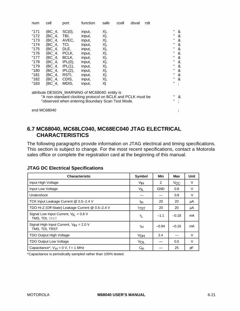
MOTOROLA M68040 USER’S MANUAL 6-21
num cell port function safe ccell dsval rslt
"171 (BC_4, SC(0), input, X), " &"172 (BC_4, TBI, input, X), " &"173 (BC_4, AVEC, input, X), " &"174 (BC_4, TCI, input, X), " &"175 (BC_4, DLE, input, X), " &"176 (BC_4, PCLK, input, X), " &"177 (BC_4, BCLK, input, X), " &"178 (BC_4, IPL(0), input, X), " &"179 (BC_4, IPL(1), input, X), " &"180 (BC_4, IPL(2), input, X), " &"181 (BC_4, RSTI, input, X), " &"182 (BC_4, CDIS, input, X), " &"183 (BC_4, MDIS, input, X) " ;
attribute DESIGN_WARNING of MC68040: entity is"A non-standard clocking protocol on BCLK and PCLK must be " &"observed when entering Boundary Scan Test Mode. " ;
end MC68040 ;
6.7 MC68040, MC68LC040, MC68EC040 JTAG ELECTRICAL CHARACTERISTICS
The following paragraphs provide information on JTAG electrical and timing specifications.This section is subject to change. For the most recent specifications, contact a Motorolasales office or complete the registration card at the beginning of this manual.
JTAG DC Electrical Specifications
Characteristic Symbol Min Max Unit
Input High Voltage VIH 2 VCC V
Input Low Voltage VIL GND 0.8 V
Undershoot — — 0.8 V
TCK Input Leakage Current @ 0.5–2.4 V Iin 20 20 µA
TDO Hi-Z (Off-State) Leakage Current @ 0.5–2.4 V ITST 20 20 µA
Signal Low Input Current, VIL = 0.8 VTMS, TDI, TRST
IL –1.1 –0.18 mA
Signal High Input Current, VIH = 2.0 VTMS, TDI, TRST
IH –0.94 –0.16 mA
TDO Output High Voltage VOH 2.4 — V
TDO Output Low Voltage VOL — 0.5 V
Capacitance*, Vin = 0 V, f = 1 MHz Cin — 25 pF
*Capacitance is periodically sampled rather than 100% tested.
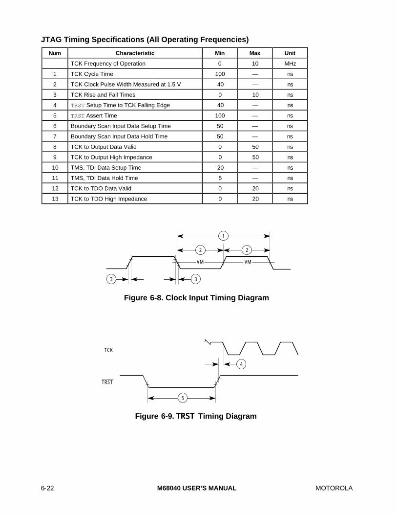
6-22 M68040 USER’S MANUAL MOTOROLA
JTAG Timing Specifications (All Operating Frequencies)
Num Characteristic Min Max Unit
TCK Frequency of Operation 0 10 MHz
1 TCK Cycle Time 100 — ns
2 TCK Clock Pulse Width Measured at 1.5 V 40 — ns
3 TCK Rise and Fall Times 0 10 ns
4 TRST Setup Time to TCK Falling Edge 40 — ns
5 TRST Assert Time 100 — ns
6 Boundary Scan Input Data Setup Time 50 — ns
7 Boundary Scan Input Data Hold Time 50 — ns
8 TCK to Output Data Valid 0 50 ns
9 TCK to Output High Impedance 0 50 ns
10 TMS, TDI Data Setup Time 20 — ns
11 TMS, TDI Data Hold Time 5 — ns
12 TCK to TDO Data Valid 0 20 ns
13 TCK to TDO High Impedance 0 20 ns
VIL
VIH
3 3
VM VM
2 2
1
Figure 6-8. Clock Input Timing Diagram
VIH
4
TRST
5
TCK
Figure 6-9. TRST Timing Diagram
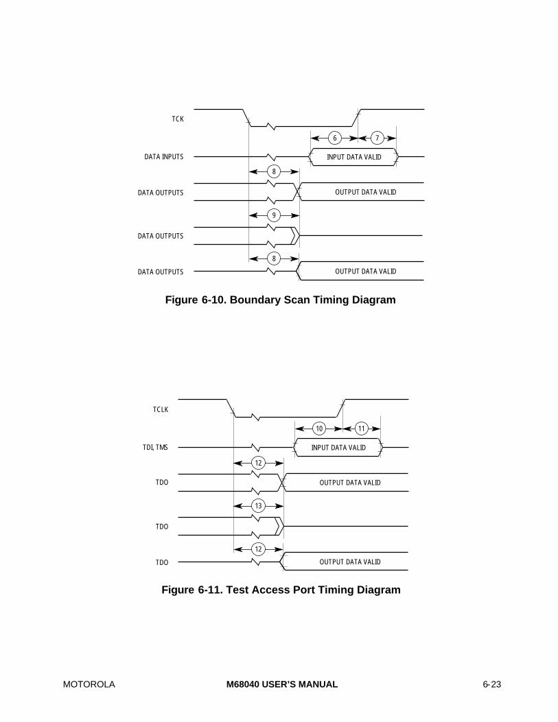
MOTOROLA M68040 USER’S MANUAL 6-23
TCK
DATA INPUTS
DATA OUTPUTS
DATA OUTPUTS
DATA OUTPUTS
8
9
8
6
VIHVIL
INPUT DATA VALID
OUTPUT DATA VALID
OUTPUT DATA VALID
7
Figure 6-10. Boundary Scan Timing Diagram
TCLK
TDI, TMS
TDO
TDO
TDO
12
13
12
10
VIHVIL
INPUT DATA VALID
OUTPUT DATA VALID
OUTPUT DATA VALID
11
Figure 6-11. Test Access Port Timing Diagram

6-24 M68040 USER’S MANUAL MOTOROLA

MOTOROLA M68040 USER’S MANUAL 7-1
SECTION 7BUS OPERATION
The M68040 bus interface supports synchronous data transfers between the processorand other devices in the system. This section provides a functional description of the bus,the signals that control the bus, and the bus cycles provided for data transfer operations.Operation of the bus is defined for transfers initiated by the processor as a bus master andfor transfers initiated by an alternate bus master, which the processor snoops as a slavedevice. Descriptions of the error and halt conditions, bus arbitration, and the resetoperation are also included. For timing specifications, refer to Section 11 MC68040Electrical and Thermal Characteristics.
NOTE
For the MC68040V, MC68LC040, and MC68EC040 ignore allreferences to floating-point. For the MC68EC040 andMC68EC040V ignore all references to the memorymanagement unit (MMU). Special modes of operation do notapply to these devices. Refer to Appendix A MC68LC040 andAppendix B MC68EC040 for details.
7.1 BUS CHARACTERISTICS
The M68040 uses the address bus (A31–A0) to specify the address for a data transferand the data bus (D31–D0) to transfer the data. Control signals indicate the beginning andtype of a bus cycle as well as the address space and size of the transfer. The selecteddevice then controls the length of the cycle by terminating it using the control signals.
The M68040 uses two clocks to generate timing: a processor clock (PCLK) and a busclock (BCLK). The PCLK signal is twice the frequency of the BCLK signal and is internallyphase-locked to BCLK. PCLK is also distributed throughout the device to generateadditional timing for additional edges for internal logic blocks and has no bearing on bustiming. The use of dual clock inputs allows the bus interface to operate at half the speed ofthe internal logic of the processor, requiring less stringent memory interface requirements.Since the rising edge of BCLK is used as the reference point for the phase-locked loop(PLL), all timing specifications are referenced to this edge.
Figure 7-1 illustrates the general relationship between the two clock signals and mostinput and output signals. The rising edge of the internally phase-locked PCLK is alignedwith the rising edge of BCLK, and the two PCLK cycles corresponding to each BCLK cycleare divided into four states, T1–T4. Most outputs change during state T4, whethertransitioning between a driven and high-impedance state or switching between assert and

7-2 M68040 USER’S MANUAL MOTOROLA
negate logic levels. The exceptions to this rule are the TIP, TA, and BB signals thattransition between logic levels during T4 but transition from a driven state to a high-impedance state during T1. The input setup time (tsu), input hold time (thi), output holdtime (tho), and delay time (td) illustrated in Figure 7-1 are described in the AC electricaltiming specifications in Section 11 MC68040 Electrical and Thermal Characteristics.
OUTPUTS
INPUTS
BCLK
T1 T2 T3 T4 T1INTERNALLY
PHASE-LOCKED PCLK
tho'
t d
t d'tho
tsuthi
= Required input setup time relative to BCLK rising edge. tsu = Required input hold time relative to BCLK rising edge. thi
= Output hold time relative to BCLK rising edge. thotho' = Output hold time relative to BCLK rising edge; = –1/2 PCLK.tho' th
= Propagation delay of signal relative to BLK rising edge. td = Propagation delay of signal relative to PCLK falling edge. td' ; = –1/2 PCLKt d' td
except for TIP, TA, BB when used as outputs.
NOTES:1.2.
3.4.5.6.
Figure 7-1. Signal Relationships to Clocks
Inputs to the M68040 (other than the IPL2–IPL0 and RSTI signals) are synchronouslysampled and must be stable during the sample window defined by tsu, thi, and tho (seeFigure 7-1) to guarantee proper operation. The asynchronous IPL≈ and RSTI signals arealso sampled on the rising edge of BCLK, but are internally synchronized to resolve theinput to a valid level before using it. Since the timing specifications for the M68040 arereferenced to the rising edge of BCLK, they are valid only for the specified operatingfrequency and must be scaled for lower operating frequencies.

MOTOROLA M68040 USER’S MANUAL 7-3
7.2 DATA TRANSFER MECHANISM
Figure 7-2 illustrates how the bus designates operands for transfers on a byte boundarysystem. The integer unit handles floating-point operands as a sequence of related long-word operands. These designations are used in the figures and descriptions that follow.
31 0
LONG-WORD OPERAND
WORD OPERAND
BYTE OPERAND
24 23 16 15 8 7
MOST SIGNIFICANT BYTE LEAST SIGNIFICANT BYTE
MOST SIGNIFICANT BYTE LEAST SIGNIFICANT BYTE
BYTE 3 BYTE 2 BYTE 1 BYTE 0
Figure 7-2. Internal Operand Representation
Figure 7-3 illustrates general multiplexing between an internal register and the externalbus. The internal register connects to the external data bus through the internal data busand multiplexer. The data multiplexer establishes the necessary connections for differentcombinations of address and data sizes.
Unlike the MC68020 and MC68030 processors, the M68040 does not support dynamicbus sizing and expects the referenced device to accept the requested access width. TheMC68150 dynamic bus sizer is designed to allow the 32-bit M68040, MC68EC040,MC68LC040 bus to communicate bidirectionally with 32-, 16-, or 8-bit peripherals andmemories. It dynamically recognizes the size of the selected peripheral or memory deviceand then reads or writes the appropriate data from that location. Refer to MC68150/D,MC68150 Dynamic Bus Sizer, for information on this device.
Blocks of memory that must be contiguous, such as for code storage or program stacks,must be 32 bits wide. Byte- and word-sized I/O ports that return an interrupt vector duringinterrupt acknowledge cycles must be mapped into the low-order 8 or 16 bits, respectively,of the data bus.
The multiplexer takes the four bytes of the 32-bit bus transfer and routes them to theirrequired positions. For example, byte 0 would normally be routed to D31–D24, but it canalso be routed to any other byte position supporting a misaligned data transfer. The sameis true for any of the other operand bytes. The transfer size (SIZ0 and SIZ1) and byteoffset (A1 and A0) signals determine the positioning of the bytes (see Table 7-1). The sizeindicated on the SIZx signals corresponds to the size of the operand transfer for the entirebus cycle. During an operand transfer, A31–A2 indicate the long-word base address forthe first byte of the operand to be accessed; A1 and A0 indicate the byte offset from thebase. For a burst-inhibited line transfer, A1 and A0 for each of the four accesses (theburst-inhibited line transfer and three long-word transfers) are copied from the lowest twobits of the access address used to initiate the line transfer.

7-4 M68040 USER’S MANUAL MOTOROLA
REGISTER
ADDRESS $xxxxxxx0
EXTERNAL DATA BUS
31 024 23 16 15 8 7
BYTE 3 BYTE 2 BYTE 1 BYTE 0
ROUTINGMULTIPLEXER
31 024 23 16 15 8 7
EXTERNAL BUS
INTERNAL TO THE MC68040
BYTE 3 BYTE 2 BYTE 1 BYTE 0
D31–D24 D23–D16 D15–D8 D7–D0
Figure 7-3. Data Multiplexing
Table 7-1 lists the combinations of the SIZx, A1, and A0 signals, collectively called byteenable signals, that are used for each of the four sections of the data bus. In the table,BYTEn indicates the data bus section that is active, the portion of the requested operandthat is read or written during that bus transfer. For line transfers, all bytes are valid aslisted and can correspond to portions of the requested operand or to data required to fillthe remainder of the cache line. The bytes labeled with a dash are not required; they areignored on read transfers and driven with undefined data on write transfers. Not selectingthese bytes prevents incorrect accesses in sensitive areas such as I/O devices. Figure 7-4illustrates a logic diagram for one method for generating byte enable signals from theSIZx, A1, and A0 and the associated PAL equation. These byte enable signals can becombined with the address decode logic.
Table 7-1. Data Bus Requirements for Read and Write Cycles
Transfer Signal Encodings Active Data Bus Sections
Size SIZ1 SIZ0 A1 A0 D31–D24 D23–D16 D15–D8 D7–D0
Byte 0000
1111
0011
0101
BYTEn———
—BYTEn
——
——
BYTEn—
———
BYTEn
Word 11
00
01
00
BYTEn—
BYTEn—
—BYTEn
—BYTEn
Long Word 0 0 X X BYTEn BYTE n BYTEn BYTEn
Line 1 1 X X BYTEn BYTEn BYTEn BYTEn

MOTOROLA M68040 USER’S MANUAL 7-5
A0A1
SIZ0SIZ1
UPPER UPPER DATA SELECT D31–D24
UPPER MIDDLE DATA SELECT D23–D16
LOWER MIDDLE DATA SELECT D15–D8
LOWER LOWER DATA SELECT D7–D0
PAL16L8 U1 MC68040 Byte Data Select Generation. Motorola Worldwide Marketing Training Organization A0 A1 SIZ0 SIZ1 NC NC NC NC NC GND NC UUD UMD LMD LLD NC NC NC NC VCC
/UUD = /A0 * /A1 + /SIZ1 * /SIZ0 + SIZ1 * SIZ0
; directly addressed, any size ; enable every byte for long word size ; enable every byte for line size ; directly addressed, any size ; word aligned, size is word or line ; enable every byte for long word size ; enable every byte for line size ; directly addressed, any size ; enable every byte for long word size ; enable every byte for line size ; directly addressed, any size ; word aligned, word or line size ; enable every byte for long word size ; enable every byte for line size
/UMD = A0 * /A1 + /A1 * /SIZ1 + SIZ1 * SIZ0 + /SIZ1 * /SIZ0/LMD = /A0 * /A1 + /SIZ1 * /SIZ0 + SIZ1 * SIZ0/LLD = A0 * /A1 + /A1 * /SIZ1 + SIZ1 * SIZ0 + /SIZ1 * /SIZ0
Figure 7-4. Byte Enable Signal Generation and PAL Equation
A brief summary of the bus signal encodings for each access type is listed in Table 7-2.Additional information on the encodings for the M68040 signals can be found in Section 5Signal Description.

7-6 M68040 USER’S MANUAL MOTOROLA
Table 7-2. Summary of Access Types versus Bus Signal Encodings
BusSignal
Data CachePush
Access
NormalData/Code
Access
TableSearchAccess
MOVE16Access
AlternateAccess
InterruptAcknowledge
BreakpointAcknowledge
A31–A0 AccessAddress
AccessAddress
EntryAddress
AccessAddress
AccessAddress
$FFFFFFFF $00000000
UPA1, UPA0 $0 MMUSource1
$0 MMUSource1
$0 $0 $0
SIZ1, SIZ0 L/Line B/W/L/Line Long Word Line B/W/L Byte Byte
TT1, TT0 $0 $0 $0 $1 $2 $3 $3
TM4–TM2 $0 $1,2,5, or 6 $3 or 4 $1 or 5 FunctionCode
Int. Level $1–7 $0
TLN1, TLN0 Cache SetEntry
Cache SetEntry2
Undefined Undefined Undefined Undefined Undefined
R/W Write Read/Write Read/Write Read/Write Read/Write Read Read
LOCKLOCKE
Negated Asserted/Negated3
Asserted/Negated3
Negated Negated Negated Negated
CIOUT Negated MMUSource1
Negated MMUSource1
Asserted Negated Negated
NOTES1. The UPA1, UPA0, and CIOUT signals are determined by the U1, U0 data and CM bit fields, respectively,
corresponding to the access address.2. The TLNx signals are defined only for normal push accesses and normal data line read accesses.3. The LOCK signal is asserted during TAS, CAS, and CAS2 operand accesses and for some table search update
sequences. LOCKE is asserted for the last transfer of each locked sequence of transfers.4. Refer to Section 5 Signal Description for definitions of the TMx signal encodings for normal, MOVE16,
and alternate accesses.
7.3 MISALIGNED OPERANDS
All M68040 data formats can be located in memory on any byte boundary. A byte operandis properly aligned at any address; a word operand is misaligned at an odd address; and along word is misaligned at an address that is not evenly divisible by 4. However, sinceoperands can reside at any byte boundary, they can be misaligned. Although the M68040does not enforce any alignment restrictions for data operands (including PC relative dataaddressing), some performance degradation occurs when additional bus cycles arerequired for long-word or word operands that are misaligned. For maximum performance,data items should be aligned on their natural boundaries. All instruction words andextension words must reside on word boundaries. Attempting to prefetch an instructionword at an odd address causes an address error exception. Refer to Section 8 ExceptionProcessing for details on address error exceptions.
The M68040 data memory unit converts misaligned operand accesses that arenoncachable to a sequence of aligned accesses. These aligned accesses are then sent tothe bus controller for completion, always resulting in aligned bus transfers. Misalignedoperand accesses that miss in the data cache are cachable and are not aligned beforeline filling. Refer to Section 4 Instruction and Data Caches for details on line fill and thedata cache.
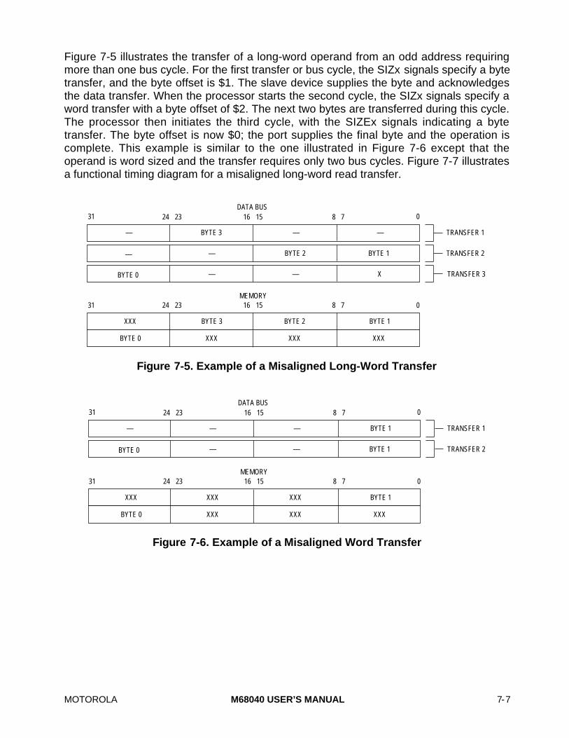
MOTOROLA M68040 USER’S MANUAL 7-7
Figure 7-5 illustrates the transfer of a long-word operand from an odd address requiringmore than one bus cycle. For the first transfer or bus cycle, the SIZx signals specify a bytetransfer, and the byte offset is $1. The slave device supplies the byte and acknowledgesthe data transfer. When the processor starts the second cycle, the SIZx signals specify aword transfer with a byte offset of $2. The next two bytes are transferred during this cycle.The processor then initiates the third cycle, with the SIZEx signals indicating a bytetransfer. The byte offset is now $0; the port supplies the final byte and the operation iscomplete. This example is similar to the one illustrated in Figure 7-6 except that theoperand is word sized and the transfer requires only two bus cycles. Figure 7-7 illustratesa functional timing diagram for a misaligned long-word read transfer.
DATA BUS31 0
— BYTE 3 — —
— — BYTE 2 BYTE 1
BYTE 0 — — X
MEMORY31 0
XXX BYTE 3 BYTE 2 BYTE 1
BYTE 0 XXX XXX XXX
TRANSFER 1
TRANSFER 2
TRANSFER 3
24 23 16 15 8 7
24 23 16 15 8 7
Figure 7-5. Example of a Misaligned Long-Word Transfer
DATA BUS31 0
— — — BYTE 1
BYTE 0 — — BYTE 1
MEMORY31 0
XXX XXX XXX BYTE 1
BYTE 0 XXX XXX XXX
TRANSFER 1
TRANSFER 2
24 23 16 15 8 7
24 23 16 15 8 7
Figure 7-6. Example of a Misaligned Word Transfer

7-8 M68040 USER’S MANUAL MOTOROLA
A31–A2
BCLK
BYTE
SIZ1
TT1, TT0
TM2–TM0
D31–D24
UPA1, UPA0
CIOUT
TS
TIP
TA
A1
A0
SIZ0
WORD
D23–D16
D15–D8
D7–D0
BYTE 0
BYTE 1
BYTE 2
BYTE 3
BYTE
BYTE READ
WORD READ
BYTE READ
R/W
C1 C2 C1 C2 C1 C2
Figure 7-7. Misaligned Long-Word Read Transfer Timing

MOTOROLA M68040 USER’S MANUAL 7-9
The combination of operand size and alignment determines the number of bus cyclesrequired to perform a particular memory access. Table 7-3 lists the number of bus cyclesrequired for different operand sizes with all possible alignment conditions for read andwrite cycles. The table confirms that alignment significantly affects bus cycle throughputfor noncachable accesses. For example, in Figure 7-5 the misaligned long-word operandtook three bus cycles because the byte offset = $1. If the byte offset = $0, then it wouldhave taken one bus cycle. The M68040 system designer and programmer should accountfor these effects, particularly in time-critical applications.
Table 7-3. Memory Alignment Influence onNoncachable and Write-Through Bus Cycles
Number of Bus Cycles
Transfer Size $0* $1* $2* $3*
Instruction 1 N/A N/A N/A
Byte Operand 1 1 1 1
Word Operand 1 2 1 2
Long-Word Operand 1 3 2 3
*Where the byte offset (A1 and A0) equals this encoding.
The processor always prefetches instructions by reading a long word from a half-lineaddress (A2–A0 = $0), regardless of alignment. When the required instruction begins atthe second long word, the processor attempts to fetch the entire half-line (two long words)although the second long word contains the required instruction.
7.4 PROCESSOR DATA TRANSFERS
The transfer of data between the processor and other devices involves the address bus,data bus, and control signals. The address and data buses are normally parallel,nonmultiplexed buses, supporting byte, word, long-word, and line (16-byte) bus cycles.Line transfers are normally performed using an efficient burst transfer, which provides aninitial address and time-multiplexes the data bus to transfer four long words of informationto or from the slave device. Slave devices that do not support bursting can burst-inhibit thefirst long word of a line transfer, forcing the bus master to complete the access using threeadditional long-word bus cycles. All bus input and output signals are synchronous to therising edge of the BCLK signal. The M68040 moves data on the bus by issuing controlsignals and using a handshake protocol to ensure correct data movement. The followingparagraphs describe the bus cycles for byte, word, long-word, and line read, write, andread-modify-write transfers.

7-10 M68040 USER’S MANUAL MOTOROLA
7.4.1 Byte, Word, and Long-Word Read Transfers
During a read transfer, the processor receives data from a memory or peripheral device.Since the data read for a byte, word, or long-word access is not placed in either of theinternal caches by definition, the processor ignores the level on the transfer cache inhibit(TCI) signal when latching the data. The bus controller performs byte, word, and long-wordread transfers for the following cases:
• Accesses to a disabled cache.
• Accesses to a memory page that is specified noncachable.
• Accesses that are implicitly noncachable (read-modify-write accesses and accessesto an alternate logical address space via the MOVES instruction).
• Accesses that do not allocate in the data cache on a read miss (table searches,exception vector fetches, and exception stack deallocation for an RTE instruction).
• The first transfer of a line read is terminated with transfer burst inhibit (TBI), forcingcompletion of the line access using three additional long-word read transfers.
Figure 7-8 is a flowchart for byte, word, and long-word read transfers. Bus operations aresimilar for each case and vary only with the size indicated and the portion of the data busused for the transfer. Figure 7-9 is a functional timing diagram for byte, word, and long-word read transfers.
ADDRESS DEVICE
1) LATCH DATA
ACQUIRE DATA
START NEXT CYCLE
PROCESSOR EXTERNAL DEVICE
PRESENT DATA
TERMINATE CYCLE
1) DECODE ADDRESS 2) PLACE DATA ON APPROPRIATE BYTES OF D31–D0 BASED ON SIZEx, A0, AND A1 3) ASSERT TA
1) REMOVE DATA FROM D31–D0 2) NEGATE TA
1) SET R/W TO READ 2) DRIVE ADDRESS ON A31–A0 3) DRIVE USER PAGE ATTRIBUTES ON UPA1, UPA0 4) DRIVE SIZE ON SIZ1, SIZ0 (BYTE, WORD, OR LONG WORD) 5) DRIVE TRANSFER TYPE ON TT1, TT0 6) DRIVE TRANSFER MODIFIER ON TM2–TM0 7) CIOUT BECOMES VALID 8) ASSERT TS FOR ONE CLOCK 9) ASSERT TIP
Figure 7-8. Byte, Word, and Long-Word Read Transfer Flowchart

MOTOROLA M68040 USER’S MANUAL 7-11
C1 C2
A31–A2
BCLK
BYTE
SIZ1
TT1, TT0
TM2–TM0
D31–D24
UPA1, UPA0
CIOUT
TS
TIP
TA
R/W
A1
A0
SIZ0
LONG
D23–D16
D15–D8
D7–D0
BYTE READ WORD READ WITH WAIT
LONG-WORD READ
C1 CW C1 C2C2
WORD
Figure 7-9. Byte, Word, and Long-WordRead Transfer Timing

7-12 M68040 USER’S MANUAL MOTOROLA
Clock 1 (C1)The read cycle starts in C1. During the first half of C1, the processor places valid valueson the address bus and transfer attributes. For user and supervisor mode accesses,which the corresponding memory unit translates, the user-programmable attributesignals (UPAx) are driven with the values from the matching user bits (U1 and U0). Thetransfer type (TTx) and transfer modifier (TMx) signals identify the specific access type.The read/write (R/W) signal is driven high for a read cycle. Cache inhibit out (CIOUT) isasserted since the access is identified as noncachable. Refer to Section 3 MemoryManagement Unit (Except MC68EC040 and MC68EC040V) for information on theM68040 and MC68LC040 memory units and Appendix B MC68EC040 for informationon the MC68EC040 memory unit.
The processor asserts transfer start (TS) during C1 to indicate the beginning of a buscycle. If not already asserted from a previous bus cycle, the transfer in progress (TIP)signal is also asserted at this time to indicate that a bus cycle is active.
Clock 2 (C2)During the first half of the clock after C1, the processor negates TS. The selectedperipheral device uses R/W, SIZ1, SIZ0, A1, and A0 to place its information on the databus. With the exception of the R/W signal, these signals also select any or all of theoperand bytes (D31–D24, D23–D16, D15–D8, and D7–D0). If the first clock after C1 isnot a wait state (CW), then the selected peripheral device asserts the transferacknowledge (TA) signal.
At the end of the first clock cycle after C1, the processor samples the level of TA andlatches the current value on the data bus; the bus cycle terminates, and the data ispassed to the processor’s appropriate memory unit if TA is asserted. If T A is notrecognized asserted at the end of the clock cycle, the processor ignores the data andinserts a wait state instead of terminating the transfer. The processor continues tosample TA on successive rising edges of BCLK until TA is recognized asserted. Thedata is then passed to the processor’s appropriate memory unit.
When the processor recognizes TA at the end of a clock and terminates the bus cycle,TIP remains asserted if the processor is ready to begin another bus cycle. Otherwise,the processor negates TIP during the first half of the next clock.
7.4.2 Line Read Transfer
The processor uses line read transfers to access a 16-byte operand for a MOVE16instruction and to support cache line filling. A line read accesses a block of four longwords, aligned to a 16-byte memory boundary, by supplying a starting address that pointsto one of the long words and requiring the memory device to sequentially drive each longword on the data bus. The selected device must internally increment A3 and A2 of thesupplied address for each transfer, causing the address to wrap around at the end of theblock. The address and transfer attributes supplied by the processor remain stable duringthe transfers, and the selected device terminates each transfer by driving the long word on

MOTOROLA M68040 USER’S MANUAL 7-13
the data bus and asserting TA. A line transfer performed in this manner with a singleaddress is referred to as a line burst transfer.
The M68040 also supports burst-inhibited line transfers for memory devices that areunable to support bursting. For this type of bus cycle, the selected device supplies the firstlong word pointed to by the processor address and asserts transfer burst inhibit (TBI) withTA for the first transfer of the line access. The processor responds by terminating the lineburst transfer and accessing the remainder of the line, using three long-word read buscycles. Although the selected device can then treat the line transfer as four, independent,long-word bus cycles, the bus controller still handles the four transfers as a single linetransfer and does not allow other unrelated processor accesses or bus arbitration tointervene between the transfers. TBI is ignored after the first long-word transfer.
Line reads to support cache line filling can be cache inhibited by asserting transfer cacheinhibit (TCI) with TA for the first long-word transfer of the line. The assertion of TCI doesnot affect completion of the line transfer, but the bus controller latches and passes it to thememory controller for use. TCI is ignored after the first long-word transfer of a line bursttransfer and during the three long-word bus cycles for a burst-inhibited line transfer.
The address placed on the address bus by the processor for line transfers does notnecessarily point to the most significant byte of each long word because for a line read, A1and A0 are copied from the original operand address supplied to the memory unit by theinteger unit. These two bits are also unchanged for the three long-word bus cycles for aburst-inhibited line transfer. The selected device should ignore A1 and A0 for long-wordand line read transfers.
The address of an instruction fetch will always be aligned to a half-line boundary($XXXXXXX0 or $XXXXXXX8); therefore, compilers should attempt to locate branchtargets on half-line boundaries to minimize branch stalls. For example, if the target of abranch is a two-word instruction located at $1000000C, the following burst sequence willoccur upon a cache miss: $10000008, $1000000C, $10000000, then $10000004. Theinternal pipeline of the M68040 stalls until the second access of the burst (the address ofthe instruction to be executed) has completed. Figures 7-10 and 7-11 illustrate a flowchartand functional timing diagram for a line read bus transfer.

7-14 M68040 USER’S MANUAL MOTOROLA
UNTIL FOUR LONG WORDS TRANSFERRED
1) NEGATE TIP (IF REQUIRED)
WHEN FOUR LONG WORDS TRANSFERRED
ADDRESS DEVICE
END OF BURST
START NEXT CYCLE
1) SET R/W TO READ 2) DRIVE ADDRESS ON A31–A0 3) DRIVE USER PAGE ATTRIBUTES ON UPA1, UPA0 4) DRIVE SIZE ON SIZ1, SIZ0 (LINE) 5) DRIVE TRANSFER TYPE ON TT1, TT0 6) DRIVE TRANSFER MODIFIER ON TM2–TM0 7) CIOUT BECOMES VALID 8) ASSERT TS FOR ONE CLOCK 9) ASSERT TIP
PROCESSOR EXTERNAL DEVICE
PRESENT DATA
TERMINATE CYCLE
1) DECODE ADDRESS 2) PLACE DATA ON D31–D0 3) ASSERT TA
1) REMOVE DATA FROM D31–D0 2) NEGATE TA (IF NECESSARY) 3) INCREMENT ADDRESS BITS A3, A2 (IF NECESSARY)
1) LATCH DATA 2) SAMPLE TBI AND TCI (FOR FIRST TRANSFER)
ACQUIRE DATA
Figure 7-10. Line Read Transfer Flowchart

MOTOROLA M68040 USER’S MANUAL 7-15
A31–A4
BCLK
SIZ1, SIZ0
TT1, TT0
TM2–TM0
D31–D0
UPA1, UPA0
CIOUT
TS
TIP
TA
R/W
A3
A2–A0
NOTE: The selected device increments the value of A3 and A2.
10 11 0001
C1 C2 C3 C4 C5
TCI
A3, A2 =
Figure 7-11. Line Read Transfer Timing
Clock 1 (C1)The line read cycle starts in C1. During the first half of C1, the processor places validvalues on the address bus and transfer attributes. For user and supervisor modeaccesses that are translated by the corresponding memory unit, the UPAx signals aredriven with the values from the matching U1 and U0 bits. The TTx and TMx signalsidentify the specific access type. The R/W signal is driven high for a read cycle, and thesize signals (SIZx) indicate line size. CIOUT is asserted for a MOVE16 operand read ifthe access is identified as noncachable. Refer to Section 3 Memory Management Unit

7-16 M68040 USER’S MANUAL MOTOROLA
(Except MC68EC040 and MC68EC040V) for information on the M68040 andMC68LC040 memory units and Appendix B MC68EC040 for information on theMC68EC040 memory unit.
The processor asserts TS during C1 to indicate the beginning of a bus cycle. If notalready asserted from a previous bus cycle, TIP is also asserted at this time to indicatethat a bus cycle is active.
Clock 2 (C2)During the first half of the first clock after C1, the processor negates TS. The selecteddevice uses R/W , SIZ1, and SIZ0 to place the data on the data bus. (The first transfermust supply the long word at the corresponding long-word boundary.) Concurrently, theselected device asserts TA and either negates or asserts TBI to indicate it can or cannotsupport a burst transfer. At the end of the first clock cycle after C1, the processorsamples the level of TA, TBI, and TCI and latches the current value on the data bus. IfTA is asserted, the transfer terminates and the data is passed to the appropriatememory unit. If TA is not recognized asserted, the processor ignores the data andinserts wait states instead of terminating the transfer. The processor continues tosample TA, TBI, and TCI on successive rising edges of BCLK until TA is recognizedasserted. The latched data and the level on TCI are then passed to the appropriatememory unit.
If TBI was negated with TA, the processor continues the cycle with C3. Otherwise, if TBI
was asserted, the line transfer is burst inhibited, and the processor reads the remainingthree long words using long-word read bus cycles. The processor increments A3 andA2 for each read, and the new address is placed on the address bus for each bus cycle.Refer to 7.4.1 Byte, Word, and Long-Word Read Transfers for information on long-word reads. If no wait states are generated, a burst-inhibited line read completes ineight clocks instead of the five required for a burst read.
Clock 3 (C3)The processor holds the address and transfer attribute signals constant during C3. Theselected device must increment A3 and A2 to reference the next long word to transfer,place the data on the data bus, and assert TA. At the end of C3, the processor samplesthe level of TA and latches the current value on the data bus. If TA is asserted, thetransfer terminates, and the second long word of data is passed to the appropriatememory unit. If TA is not recognized asserted at the end of C3, the processor ignoresthe latched data and inserts wait states instead of terminating the transfer. Theprocessor continues to sample TA on successive rising edges of BCLK until it isrecognized. The latched data is then passed to the appropriate memory unit.
Clock 4 (C4)This clock is identical to C3 except that once TA is recognized asserted, the latchedvalue corresponds to the third long word of data for the burst.

MOTOROLA M68040 USER’S MANUAL 7-17
Clock 5 (C5)This clock is identical to C3 except that once TA is recognized, the latched valuecorresponds to the third long word of data for the burst. After the processor recognizesthe last TA assertion and terminates the line read bus cycle, TIP remains asserted if theprocessor is ready to begin another bus cycle. Otherwise, the processor negates TIP
during the first half of the next clock.
Figures 7-12 and 7-13 illustrate a flowchart and functional timing diagram for a burst-inhibited line read bus cycle.

7-18 M68040 USER’S MANUAL MOTOROLA
PRESENT DATA
1) LATCH DATA 2) SAMPLE TBI AND TCI 3) RECOGNIZE TBI ASSERTED
1) REMOVE DATA FROM D31–D0 2) NEGATE TA
TERMINATE CYCLE
1) SET R/W TO READ 2) DRIVE ADDRESS ON A31–A0 3) DRIVE USER PAGE ATTRIBUTES ON UPA1, UPA0 4) DRIVE SIZE ON SIZ1, SIZ0 (LINE) 5) DRIVE TRANSFER TYPE ON TT1, TT0 6) DRIVE TRANSFER MODIFIER ON TM2–TM0 7) CIOUT BECOMES VALID 8) ASSERT TS FOR ONE CLOCK 9) ASSERT TIP
ADDRESS DEVICE
ACQUIRE DATA
START NEXT CYCLE
PROCESSOR EXTERNAL DEVICE
1) DECODE ADDRESS 2) PLACE DATA ON D31–D0 3) ASSERT TA AND TBI
1) NEGATE TIP (IF REQUIRED)
END OF LINE TRANSFER
1) INCREMENT ADDRESS BITS A3, A2 AND DRIVE NEW ADDRESS ON A31–A0 2) DRIVE SIZE ON SIZ1, SIZ0 (LONG WORD) 3) ASSERT TRANSFER START (TS) FOR ONE CLOCK
ADDRESS DEVICE
PRESENT DATA
1) REMOVE DATA FROM D31–D0 2) NEGATE TA
TERMINATE CYCLE
1) DECODE ADDRESS 2) PLACE DATA ON D31–D0 3) ASSERT TA
1) LATCH DATA
ACQUIRE DATA
WHEN THREE LONG WORDS TRANSFERRED
UNTIL THREE LONG WORDS TRANSFERRED
Figure 7-12. Burst-Inhibited Line Read Transfer Flowchart

MOTOROLA M68040 USER’S MANUAL 7-19
A31–A4
BCLK
TT1, TT0
TM2–TM0
D31–D0
UPA1, UPA0
CIOUT
TS
TIP
TA
R/W
A3
A2
A1, A0
SIZ1, SIZ0
TLN1, TLN0
LINE LONG LONG LONG
TBI
TCI
INHIBITED LINE READ
LONG-WORD READ
LONG-WORD READ
LONG-WORD READ
C1 C2 C3 C4 C6 C7C5 C8
Figure 7-13. Burst-Inhibited Line Read Transfer Timing

7-20 M68040 USER’S MANUAL MOTOROLA
7.4.3 Byte, Word, and Long-Word Write Transfers
During a write transfer, the processor transfers data to a memory or peripheral device.The level on the TCI signal is ignored by the processor during all write cycles. The buscontroller performs byte, word, and long-word write transfers for the following cases:
• Accesses to a disabled cache.
• Accesses to a memory page that is specified noncachable.
• Accesses that are implicitly noncachable (read-modify-write accesses and accessesto an alternate logical address space via the MOVES instruction).
• Writes to write-through pages.
• Accesses that do not allocate in the data cache on a write miss (table updates andexception stacking).
• The first transfer of a line write is terminated with TBI, forcing completion of the lineaccess using three additional long-word write transfers.
• Cache line pushes for lines containing a single dirty long word.
Figures 7-14 and 7-15 illustrate a flowchart and functional timing diagram for byte, word,and long-word write bus transfers.
ADDRESS DEVICE
1) REMOVE DATA FROM D31–D0 2) NEGATE TIP (IF REQUIRED)
TERMINATE TRANSFER
START NEXT CYCLE
PROCESSOR EXTERNAL DEVICE
ACCEPT DATA
TERMINATE CYCLE
1) NEGATE TA
1) SET R/W TO WRITE 2) DRIVE ADDRESS ON A31–A0 3) DRIVE USER PAGE ATTRIBUTES ON UPA1, UPA0 4) DRIVE SIZE ON SIZ1, SIZ0 (BYTE, WORD, OR LONG WORD) 5) DRIVE TRANSFER TYPE ON TT1, TT0
6) DRIVE TRANSFER MODIFIER ON TM2–TM0 7) CIOUT BECOMES VALID 8) ASSERT TS FOR ONE CLOCK 9) ASSERT TIP 10) DRIVE DATA ON APPROPRIATE BYTES OF D31–D0 BASED ON SIZEx, A1, AND A0
1) DECODE ADDRESS 2) LATCH DATA ON APPROPRIATE BYTES OF D31–D0 BASED ON SIZEx, A1, AND A0 3) ASSERT TRANSFER ACKNOWLEDGE (TA)
Figure 7-14. Byte, Word, and Long-Word Write Transfer Flowchart
MOTOROLA M68040 USER’S MANUAL 7-21
A31–A0
BCLK
SIZ1, SIZ0
TT1, TT0
TM2–TM0
D31–D0
UPA1, UPA0
CIOUT
TS
TIP
TA
R/W
LONG
LONG-WORD WRITE
C1 C2
Figure 7-15. Long-Word Write Transfer Timing
Clock 1 (C1)The write cycle starts in C1. During the first half of C1, the processor places valid valueson the address bus and transfer attributes. For user and supervisor mode accesses,which the corresponding memory unit translates, the UPAx signals are driven with thevalues from the U1 and U0 bits for the area. The TTx and TMx signals identify thespecific access type. The R/W signal is driven low for a write cycle. CIOUT is asserted ifthe access is identified as noncachable or if the access references an alternate addressspace. Refer to Section 3 Memory Management Unit (Except MC68EC040 andMC68EC040V) for information on the M68040 and MC68LC040 memory units andAppendix B MC68EC040 for information on the MC68EC040 memory unit.
The processor asserts TS during C1 to indicate the beginning of a bus cycle. If notalready asserted from a previous bus cycle, the TIP signal is also asserted at this timeto indicate that a bus cycle is active.

7-22 M68040 USER’S MANUAL MOTOROLA
Clock 2 (C2)During the first half of the clock after C1, the processor negates TS and drives theappropriate bytes of the data bus with the data to be written. All other bytes are drivenwith undefined values. The selected device uses R/W , SIZ1, SIZ0, A1, A0, and CIOUT
to latch only the required information on the data bus. With the exception of R/W andCIOUT, these signals also select any or all of the bytes (D31–D24, D23–D16, D15–D8,and D7–D0). If the first clock after C1 is not a wait state, then the selected peripheraldevice asserts the TA signal.
At the end of the first clock cycle after C1, the processor samples the level of TA,terminating the bus cycle if TA is asserted. If TA is not recognized asserted at the end ofthe clock cycle, the processor ignores the data and inserts a wait state instead ofterminating the transfer. The processor continues to sample TA on successive risingedges of BCLK until TA is recognized asserted. The data bus then three-states and thebus cycle ends.
When the processor recognizes TA at the clock edge and terminates the bus cycle, TIP
remains asserted if the processor is ready to begin another bus cycle. Otherwise, theprocessor negates TIP during the first half of the next clock. The processor also three-states the data bus during the first half of the next clock following termination of thewrite transfer.
7.4.4 Line Write Transfers
The processor uses line write bus cycles to access a 16-byte operand for a MOVE16instruction and to support cache line pushes. Both burst and burst-inhibited transfers aresupported. Figures 7-16 and 7-17 illustrate a flowchart and functional timing diagram for aline write bus cycle.
MOTOROLA M68040 USER’S MANUAL 7-23
1) SET R/W TO WRITE 2) DRIVE ADDRESS ON A31–A0 3) DRIVE USER PAGE ATTRIBUTES ON UPA1, UPA0 4) DRIVE SIZE ON SIZ1, SIZ0 (LINE) 5) DRIVE TRANSFER TYPE ON TT1, TT0 6) DRIVE TRANSFER MODIFIER ON TM2–TM0 7) CIOUT BECOMES VALID
ACCEPT DATA
1) DRIVE DATA ON D31–D0 2) SAMPLE TA 3) SAMPLE TBI AND TCI (FOR FIRST TRANSFER)
1) NEGATE TA (IF NECESSARY) 2) INCREMENT ADDRESS BITS A3, A2 (IF NECESSARY)
TERMINATE CYCLE
ADDRESS DEVICE
SUPPLY DATA
START NEXT CYCLE
PROCESSOR EXTERNAL DEVICE
1) DECODE ADDRESS (FIRST TRANSFER ONLY) 2) LATCH DATA ON D31–D0 3) ASSERT TA
UNTIL FOUR LONG WORDS TRANSFERRED
1) REMOVE DATA FROM D31–D0 2) NEGATE TIP (IF REQUIRED)
END OF BURST
UNTIL FOUR LONG WORDS TRANSFERRED
WHEN FOUR LONG WORDS TRANSFERRED
8) ASSERT TS FOR ONE CLOCK 9) ASSERT TIP
Figure 7-16. Line Write Transfer Flowchart
7-24 M68040 USER’S MANUAL MOTOROLA
A31–A4
BCLK
SIZ1, SIZ0
TT1, TT0
TM2–TM0
D31–D0
UPA1, UPA0
CIOUT
TS
TIP
TA
R/W
A3
A2–A0
NOTE: The selected device increments the value of A3 and A2.
10 11 0001
C1 C2 C3 C4 C5
A3, A2 =
Figure 7-17. Line Write Transfer Timing
Clock 1 (C1)The line write cycle starts in C1. During the first half of C1, the processor places validvalues on the address bus and transfer attributes. For user and supervisor modeaccesses that are translated by the corresponding memory unit, UPAx signals aredriven with the values from the matching U1 and U0 bits. The TTx and TMx signalsidentify the specific access type. The R/W signal is driven low for a write cycle, andSIZ1 and SIZ0 indicate line size. CIOUT is asserted for a MOVE16 operand read if theaccess is identified as noncachable. Refer to Section 3 Memory Management Unit(Except MC68EC040 and MC68EC040V) for information on the M68040 and

MOTOROLA M68040 USER’S MANUAL 7-25
MC68LC040 memory units and Appendix B MC68EC040 for information on theMC68EC040 memory unit.
The processor asserts TS during C1 to indicate the beginning of a bus cycle. If notalready asserted from a previous bus cycle, the TIP signal is also asserted at this timeto indicate that a bus cycle is active.
Clock 2 (C2)During the first half of the first clock after C1, the processor negates TS and drives thedata bus with the data to be written. The selected device uses R/W, SIZ1, and SIZ0 tolatch the data on the data bus. Concurrently, the selected device asserts TA and eithernegates or asserts TBI to indicate it can or cannot support a burst transfer. At the end ofthe first clock after C1, the processor samples the level of TA and TBI. If TA is asserted,the transfer terminates. If TA is not recognized asserted, the processor inserts waitstates instead of terminating the transfer. The processor continues to sample TA andTBI on successive rising edges of BCLK until TA is recognized asserted.
If TBI was negated with TA, the processor continues the cycle with C3. Otherwise, if TBI
was asserted, the line transfer is burst inhibited, and the processor writes the remainingthree long words using long-word write bus cycles. Only in this case does the processorincrement A3 and A2 for each write, and the new address is placed on the address busfor each bus cycle. Refer to 7.4.3 Byte, Word, and Long-Word Write Transfers forinformation on long-word writes. If no waits states are generated, a burst-inhibited linewrite completes in eight clocks instead of the five required for a burst write.
Clock 3 (C3)The processor drives the second long word of data on the data bus and holds theaddress and transfer attribute signals constant during C3. The selected deviceincrements A3 and A2 to reference the next long word, latches this data from the databus, and asserts TA. At the end of C3, the processor samples the level of TA; if TA isasserted, the transfer terminates. If TA is not recognized asserted at the end of C3, theprocessor inserts wait states instead of terminating the transfer. The processorcontinues to sample TA on successive rising edges of BCLK until TA is recognizedasserted.
Clock 4 (C4)This clock is identical to C3 except that the value driven on the data bus corresponds tothe third long word of data for the burst.
Clock 5 (C5)This clock is identical to C3 except that the value driven on the data bus corresponds tothe fourth long word of data for the burst. After the processor recognizes the last TA
assertion and terminates the line write bus cycle, TIP remains asserted if the processoris ready to begin another bus cycle. Otherwise, the processor negates TIP during thefirst half of the next clock. The processor also three-states the data bus during the firsthalf of the next clock following termination of the write cycle.
7-26 M68040 USER’S MANUAL MOTOROLA
7.4.5 Read-Modify-Write Transfers (Locked Transfers)
The read-modify-write transfer performs a read, conditionally modifies the data in theprocessor, and writes the data out to memory. In the M68040, this operation can beindivisible, providing semaphore capabilities for multiprocessor systems. During the entireread-modify-write sequence, the M68040 asserts the LOCK signal to indicate that anindivisible operation is occurring and asserts the LOCKE signal for the last transfer toindicate completion of the locked sequence. The external arbiter can use the LOCK andLOCKE signals to prevent arbitration of the bus during locked processor sequences.External bus arbitrations can use LOCKE to support bus arbitration between consecutiveread-modify-write cycles. A read-modify-write operation is treated as noncachable. If theaccess hits in the data cache, it invalidates a matching valid entry and pushes a matchingdirty entry. The read-modify-write transfer begins after the line push (if required) iscomplete; however, LOCK may assert during the line push bus cycle.
The TAS, CAS, and CAS2 instructions are the only M68040 instructions that utilize read-modify-write transfers. Some page descriptor updates during translation table searchesalso use read-modify-write transfers. Refer to Section 3 Memory Management Unit(Except MC68EC040 and MC68EC040V) for information about table searches.
The read-modify-write transfer for the CAS and CAS2 instructions in the M68040 differsfrom those used by previous members of the M68000 family. If an operand does notmatch one of these instructions, the M68040 still executes a single write transfer toterminate the locked sequence with LOCKE asserted. For the CAS instruction, the valueread from memory is written back; for the CAS2 instruction, the second operand read iswritten back. Figure 7-18 illustrates a functional timing diagram for a TAS instruction read-modify-write bus transfer.
Clock 1 (C1)The read cycle starts in C1. During the first half of C1, the processor places valid valueson the address bus and transfer attributes. LOCK is asserted to identify a locked read-modify-write bus cycle. For user and supervisor mode accesses, which thecorresponding memory unit translates, the UPAx signals are driven with the values fromthe matching U1 and U0 bits. The TTx and TMx signals identify the specific accesstype. R/W is driven high for a read cycle. CIOUT is asserted if the access is identified asnoncachable. The processor asserts TS during C1 to indicate the beginning of a buscycle. If not already asserted from a previous bus cycle, the TIP signal is also assertedat this time to indicate that a bus cycle is active. Refer to Section 3 MemoryManagement Unit (Except MC68EC040 and MC68EC040V) for information on theM68040 and MC68LC040 memory units and Appendix B MC68EC040 for informationon the MC68EC040 memory unit.

MOTOROLA M68040 USER’S MANUAL 7-27
C1 C2
A31–A0
BCLK
BYTE
SIZ1
TT1, TT0
TM2–TM0
D31–D24
UPA1, UPA0
CIOUT
TS
TIP
TA
R/W
SIZ0
D23–D16
D15–D8
D7–D0
CI C3 C4
LOCKE
LOCK
LOCKED TRANSFER
Undefined
Figure 7-18. Locked Transfer for TAS Instruction Timing

7-28 M68040 USER’S MANUAL MOTOROLA
Clock 2 (C2)During the first half of the first clock cycle after C1, the processor negates TS. Theselected device uses R/W , SIZ1, SIZ0, A1, and A0 to place its information on the databus. With the exception of R/W , these signals also select any or all of the bytes (D24–D31, D16–D23, D15–D8, and D7–D0). Concurrently, the selected device asserts TA. Atthe end of the first clock cycle after C1, the processor samples the level of TA andlatches the current value on the data bus. If TA is asserted, the read transfer terminates,and the latched data is passed to the appropriate memory unit. If TA is not recognizedasserted, the processor ignores the data and appends a wait state instead ofterminating the transfer. The processor continues to sample TA on successive risingedges of BCLK until TA is recognized as asserted. The latched data is then passed tothe appropriate memory unit. If more than one read cycle is required to read in theoperand(s), C1 and C2 are repeated accordingly.
When the processor recognizes TA at the end of the last read transfer for the lockedbus cycle, it negates TIP during the first half of the next clock.
Clock Idle (CI)The processor does not assert any new control signals during the idle clock states, but itmay begin the modify portion of the cycle at this time. The R/W signal remains in theread mode until C3 to prevent bus conflicts with the preceding read portion of the cycle;the data bus is not driven until C4.
Clock 3 (C3)During the first half of C3, the processor places valid values on the address bus andtransfer attributes and drives R/W low for a write cycle. The processor asserts TS toindicate the beginning of a bus cycle. The TIP signal is also asserted at this time toindicate that a bus cycle is active.
LOCKE is asserted during C3 for the last write transfer of the locked sequence. Ifmultiple write transfers are required for misaligned operands or multiple operands,LOCKE is asserted only for the final write transfer. The external arbiter can use thisindication to distinguish between two back-to-back locked bus cycles and allowarbitration between them.
Clock 4 (C4)During the first half of C4, the processor negates TS and drives the appropriate bytes ofthe data bus with the data to be written. All other bytes are driven with undefined values.The selected device uses R/W , SIZ1, SIZ0, A1, and A0 to latch the information on thedata bus. Any or all of the bytes (D31–D24, D23–D16, D15–D8, and D7–D0) areselected by SIZ1, SIZ0, A1, and A0. Concurrently, the selected device asserts TA. Atthe end of C4, the processor samples the level of TA; if TA is asserted, the bus cycleterminates. If TA is not recognized asserted at the end of C4, the processor appends await state instead of terminating the transfer. The processor continues to sample the TA
signal on successive rising edges of BCLK until it is recognized asserted.

MOTOROLA M68040 USER’S MANUAL 7-29
When the processor recognizes TA at the end of a clock, the bus cycle is terminated,but TIP remains asserted if the processor is ready to begin another bus cycle.Otherwise, the processor negates TIP during the first half of the next clock. Theprocessor also three-states the data bus during the first half of the next clock followingtermination of the write cycle. When the last write transfer is terminated, LOCKE isnegated. The processor also negates LOCK if the next bus cycle is not a read-modify-write.
7.5 ACKNOWLEDGE BUS CYCLES
Bus transfers with transfer type signals TT1 and TT0 = $3 are classified as acknowledgebus cycles. The following paragraphs describe interrupt acknowledge and breakpointacknowledge bus cycles that use this encoding.
7.5.1 Interrupt Acknowledge Bus Cycles
When a peripheral device requires the services of the M68040 or is ready to sendinformation that the processor requires, it can signal the processor to take an interruptexception. The interrupt exception transfers control to a routine that respondsappropriately. The peripheral device uses the active-low interrupt priority level signals(IPL2–IPL0) to signal an interrupt condition to the processor and to specify the priority levelfor the condition. Refer to Section 8 Exception Processing for a discussion on the IPL≈
levels and IPEND.
The status register (SR) of the M68040 contains an interrupt priority mask (I2–I0 bits). Thevalue in the interrupt mask is the highest priority level that the processor ignores. When aninterrupt request has a priority higher than the value in the mask, the processor makes therequest a pending interrupt. IPL2–IPL0 must maintain the interrupt request level until theM68040 acknowledges the interrupt to guarantee that the interrupt is recognized. TheM68040 continuously samples IPL2–IPL0 on consecutive rising edges of BCLK tosynchronize and debounce these signals. An interrupt request that is held constant for twoconsecutive clock periods is considered a valid input. Although the protocol requires thatthe request remain until the processor runs an interrupt acknowledge cycle for thatinterrupt value, an interrupt request that is held for as short a period as two clock cyclescan be recognized. Figure 7-19 is a flowchart of the procedure for making an interruptpending.

7-30 M68040 USER’S MANUAL MOTOROLA
RESET
SAMPLE AND SYNCHRONIZE IPL2–IPL0
ASSERT IPENDOTHERWISE
INTERRUPT LEVEL I2–I0, OR TRANSITION ON LEVEL 7
>
Figure 7-19. Interrupt Pending Procedure
The M68040 asserts IPEND when an interrupt request is pending. Figure 7-20 illustratesthe assertion of IPEND relative to the assertion of an interrupt level on the IPL≈ signals.IPEND signals external devices that an interrupt exception will be taken at an upcominginstruction boundary (following any higher priority exception). The IPEND signal negatesafter the processor recognizes the internal interrupt acknowledge and can precede theexternal interrupt acknowledge bus cycle.
BCLK
IPL2–IPL0
IPEND
COMPARE REQUEST WITH MASK IN SR
ASSERT IPENDIPLs RECOGNIZED
IPLs SYNCHRONIZED
Figure 7-20. Assertion of IPEND

MOTOROLA M68040 USER’S MANUAL 7-31
The M68040 takes an interrupt exception for a pending interrupt within one instructionboundary after processing any other pending exception with a higher priority. Thus, theM68040 executes at least one instruction in an interrupt exception handler beforerecognizing another interrupt request. The following paragraphs describe the various kindsof interrupt acknowledge bus cycles that can be executed as part of interrupt exceptionprocessing. Table 7-4 provides a summary of the possible interrupt acknowledgeterminations and the exception processing results.
Table 7-4. Interrupt Acknowledge Termination Summary
TA TEA AVEC Termination Condition
High High Don’t Care Insert Waits
High Low Don’t Care Take Spurious Interrupt Exception
Low High High Latch Vector Number on D7–D0 and Take Interrupt Exception
Low High Low Take Autovectored Interrupt Exception
Low Low Don’t Care Retry Interrupt Acknowledge Cycle
7.5.1.1 INTERRUPT ACKNOWLEDGE BUS CYCLE (TERMINATED NORMALLY).When the M68040 processes an interrupt exception, it performs an interrupt acknowledgebus cycle to obtain the vector number that contains the starting location of the interruptexception handler. Some interrupting devices have programmable vector registers thatcontain the interrupt vectors for the exception handlers they use. Other interruptingconditions or devices cannot supply a vector number and use the autovector bus cycledescribed in 7.5.1.2 Autovector Interrupt Acknowledge Bus Cycle.

7-32 M68040 USER’S MANUAL MOTOROLA
The interrupt acknowledge bus cycle is a read transfer. It differs from a normal read cyclein the following respects:
1. TT1 and TT0 = $3 to indicate an acknowledged bus cycle.
2. Address signals A31–A0 are set to all ones ($FFFFFFFF).
3. TM2–TM0 are set to the interrupt request level (the inverted values of IPL2–IPL0).
The responding device places the vector number on the data bus during the interruptacknowledge bus cycle, and the cycle is terminated normally with TA. Figures 7-21 and7-22 illustrate a flowchart and functional timing diagram for an interrupt acknowledge cycleterminated with TA.
ACKNOWLEDGE INTERRUPT
1) LATCH VECTOR NUMBER
ACQUIRE DATA
START NEXT CYCLE
3) DRIVE A31–A0 TO $FFFFFFFF 4) DRIVE UPA1, UPA0 TO $0 5) SET SIZE TO BYTE 6) SET TRANSFER TYPE ON TT1, TT0 TO $3 7) PLACE INTERRUPT LEVEL ON TM2–TM0
PROCESSOR EXTERNAL DEVICE
PROVIDE VECTOR INFORMATION
TERMINATE CYCLE
1) PLACE VECTOR NUMBER ON BYTE D7–D0 2) ASSERT TRANSFER ACKNOWLEDGE (TA)
1) REMOVE DATA FROM D7–D0 2) NEGATE TA
REQUEST INTERRUPT
8) NEGATE CIOUT 9) ASSERT TS FOR ONE CLOCK 10) ASSERT TIP
1) IPEND RECOGNIZED, WAIT FOR INSTRUCTION BOUNDARY 2) SET R/W TO READ
Figure 7-21. Interrupt Acknowledge Bus Cycle Flowchart

MOTOROLA M68040 USER’S MANUAL 7-33
C1 C2
A31–A0
BCLK
BYTE
SIZ1
TT1, TT0
TM2–TM0
D31–D8
UPA1, UPA0
CIOUT
TS
TIP
TA
R/W
SIZ0
D7–D0
INTERRUPT ACKNOWLEDGE
INTERRUPT LEVEL
AVEC
C1 C2
WRITE STACK
VECTOR #
Figure 7-22. Interrupt Acknowledge Bus Cycle Timing
7.5.1.2 AUTOVECTOR INTERRUPT ACKNOWLEDGE BUS CYCLE. When theinterrupting device cannot supply a vector number, it requests an automatically generatedvector (autovector). Instead of placing a vector number on the data bus and asserting TA,the device asserts the autovector (AVEC) signal with TA to terminate the cycle. AVEC isonly sampled with TA asserted. AVEC can be grounded if all interrupt requests areautovectored.
The vector number supplied in an autovector operation is derived from the interrupt prioritylevel of the current interrupt. When the AVEC signal is asserted with TA during an interruptacknowledge bus cycle, the M68040 ignores the state of the data bus and internally
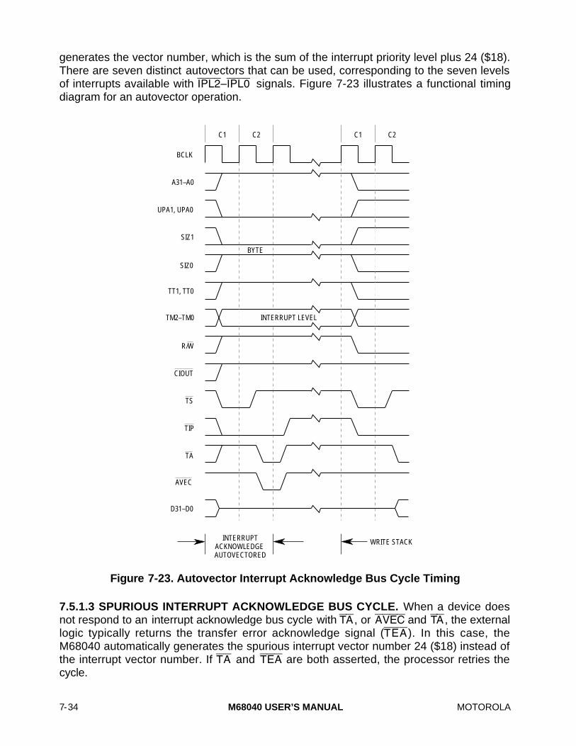
7-34 M68040 USER’S MANUAL MOTOROLA
generates the vector number, which is the sum of the interrupt priority level plus 24 ($18).There are seven distinct autovectors that can be used, corresponding to the seven levelsof interrupts available with IPL2–IPL0 signals. Figure 7-23 illustrates a functional timingdiagram for an autovector operation.
C1 C2
A31–A0
BCLK
BYTE
SIZ1
TT1, TT0
TM2–TM0
D31–D0
UPA1, UPA0
CIOUT
TS
TIP
TA
R/W
SIZ0
INTERRUPT ACKNOWLEDGE AUTOVECTORED
INTERRUPT LEVEL
AVEC
C1 C2
WRITE STACK
Figure 7-23. Autovector Interrupt Acknowledge Bus Cycle Timing
7.5.1.3 SPURIOUS INTERRUPT ACKNOWLEDGE BUS CYCLE. When a device doesnot respond to an interrupt acknowledge bus cycle with TA, or AVEC and TA, the externallogic typically returns the transfer error acknowledge signal (TEA). In this case, theM68040 automatically generates the spurious interrupt vector number 24 ($18) instead ofthe interrupt vector number. If TA and TEA are both asserted, the processor retries thecycle.

MOTOROLA M68040 USER’S MANUAL 7-35
7.5.2 Breakpoint Interrupt Acknowledge Bus Cycle
The execution of a breakpoint instruction (BKPT) generates the breakpoint interruptacknowledge bus cycle. An acknowledged access is indicated with TT1 and TT0 = $3,address A31–A0 = $00000000, and TM2–TM0 = $0. When the external device terminatesthe cycle with either TA or TEA, the processor takes an illegal instruction exception.Figures 7-24 and 7-25 illustrate a flowchart and functional timing diagram for a breakpointinterrupt acknowledge transfer.
BREAKPOINT ACKNOWLEDGE
INITIATE ILLEGAL INSTRUCTION EXCEPTION PROCESSING
1) SET R/W TO READ 2) DRIVE A31–A0 TO $00000000 3) DRIVE UPA1, UPA0 TO $0 4) SET SIZE TO BYTE 5) SET TRANSFER TYPE ON TT1, TT0 TO $3 6) SET TRANSFER MODIFIER TM2–TM0 TO $0
PROCESSOR EXTERNAL DEVICE
TERMINATE CYCLE
ASSERT TA OR TEA
1) NEGATE TA OR TEA
8) NEGATE CIOUT 9) ASSERT TS FOR ONE CLOCK 10) ASSERT TIP
Figure 7-24. Breakpoint Interrupt Acknowledge Bus Cycle Flowchart
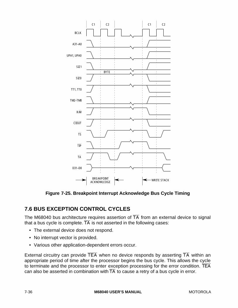
7-36 M68040 USER’S MANUAL MOTOROLA
C1 C2
A31–A0
BCLK
BYTE
SIZ1
TT1, TT0
TM2–TM0
D31–D0
UPA1, UPA0
CIOUT
TS
TIP
TA
R/W
SIZ0
BREAKPOINT ACKNOWLEDGE
C1 C2
WRITE STACK
Figure 7-25. Breakpoint Interrupt Acknowledge Bus Cycle Timing
7.6 BUS EXCEPTION CONTROL CYCLES
The M68040 bus architecture requires assertion of TA from an external device to signalthat a bus cycle is complete. TA is not asserted in the following cases:
• The external device does not respond.
• No interrupt vector is provided.
• Various other application-dependent errors occur.
External circuitry can provide TEA when no device responds by asserting TA within anappropriate period of time after the processor begins the bus cycle. This allows the cycleto terminate and the processor to enter exception processing for the error condition. TEA
can also be asserted in combination with TA to cause a retry of a bus cycle in error.

MOTOROLA M68040 USER’S MANUAL 7-37
To properly control termination of a bus cycle for a bus error or retry condition, TA andTEA must be asserted and negated for the same rising edge of BCLK. Table 7-5 lists thecontrol signal combinations and the resulting bus cycle terminations. Bus error and retryterminations during burst cycles operate as described in 7.4.2 Line Read Transfers and7.4.4 Line Write Transfers.
Table 7-5. TA and TEA Assertion Results
Case No. TA TEA Result
1 High Low Bus Error—Terminate and Take Bus Error Exception,Possibly Deferred
2 Low Low Retry Operation—Terminate and Retry
3 Low High Normal Cycle Terminate and Continue
4 High High Insert Wait States
7.6.1 Bus Errors
The system hardware can use the TEA signal to abort the current bus cycle when a faultis detected. A bus error is recognized during a bus cycle when TA is negated and TEA isasserted. When the processor recognizes a bus error condition for an access, the accessis terminated immediately. A line access that has TEA asserted for one of the four long-word transfers aborts without completing the remaining transfers, regardless of whetherthe line transfer uses a burst or burst-inhibited access.
When TEA is asserted to terminate a bus cycle, the M68040 can enter access errorexception processing immediately following the bus cycle, or it can defer processing theexception. The instruction prefetch mechanism requests instruction words from theinstruction memory unit before it is ready to execute them. If a bus error occurs on aninstruction fetch, the processor does not take the exception until it attempts to use theinstruction. Should an intervening instruction cause a branch or should a task switchoccur, the access error exception for the unused access does not occur. Similarly, if a buserror is detected on the second, third, or fourth long-word transfer for a line read access,an access error exception is taken only if the execution unit is specifically requesting thatlong word. Otherwise, the line is not placed in the cache, and the processor repeats theline access when another access references the line. If a misaligned operand spans twolong words in a line, a bus error on either the first or second transfer for the line causesexception processing to begin immediately. A bus error termination for any write accessesor for read accesses that reference data specifically requested by the execution unitcauses the processor to begin exception processing immediately. Refer to Section 8Exception Processing for details of access error exception processing.
When a bus error terminates an access, the contents of the corresponding cache can beaffected in different ways, depending on the type of access. For a cache line read toreplace a valid instruction or data cache line, the cache line being filled is invalidatedbefore the bus cycle begins and remains invalid if the replacement line access isterminated with a bus error. If a dirty data cache line is being replaced and a bus erroroccurs during the replacement line read, the dirty line is restored from an internal push

7-38 M68040 USER’S MANUAL MOTOROLA
buffer into the cache to eliminate an unnecessary push access. If a bus error occursduring a data cache push, the corresponding cache line remains valid (with the new linedata) if the line push follows a replacement line read, or is invalidated if a CPUSHinstruction explicitly forces the push. Write accesses to memory pages specified as write-through by the data memory unit update the corresponding cache line before accessingmemory. If a bus error occurs during a memory access, the cache line remains valid withthe new data. Figure 7-26 illustrates a functional timing diagram of a bus error on a wordwrite access causing an access error exception. Figure 7-27 illustrates a functional timingdiagram of a bus error on a line read access that does not cause an access errorexception.
A physical bus error during an FSAVE instruction results in corruption of the floating-pointstate frame. This is not a serious limitation since, prior to writing the stack frame, theM68040 ensures that the pages required for the floating-point state frame are resident.Therefore, only a physical bus error can cause an access error during the stacking of thestate frame. In a normal application, writes caused by the processor should not result in aphysical bus error since the logical address space has already been translated andallocated. Since there should be no parity errors caused by processor write accesses, onlyspurious assertions of the TEA pin can cause physical bus errors. Furthermore, becauseFSAVE instructions usually place the state frame on the system stack, the occurrence of aphysical bus error when using the system stack indicates a serious hardware error.

MOTOROLA M68040 USER’S MANUAL 7-39
C1 C2
A31–A0
BCLK
WORD
SIZ1
TT1, TT0
TM2–TM0
D31–D0
UPA1, UPA0
CIOUT
TS
TIP
TA
R/W
SIZ0
WRITE CYCLE
C1 C2
WRITE STACK
TEA
Figure 7-26. Word Write Access Terminated with TEA Timing

7-40 M68040 USER’S MANUAL MOTOROLA
A31–A4
BCLK
SIZ1, SIZ0
TT1, TT0
TM2–TM0
D31–D0
UPA1, UPA0
CIOUT
TS
TIP
TA
R/W
A3
A2–A0
NOTE: The selected device increments the value on A3 and A2.
10 1101
C1 C2 C3 C4
TBI
TEA
TEA ENDS BURST – NO EXCEPTION TAKEN
A3, A2 =
Figure 7-27. Line Read Access Terminated with TEA Timing
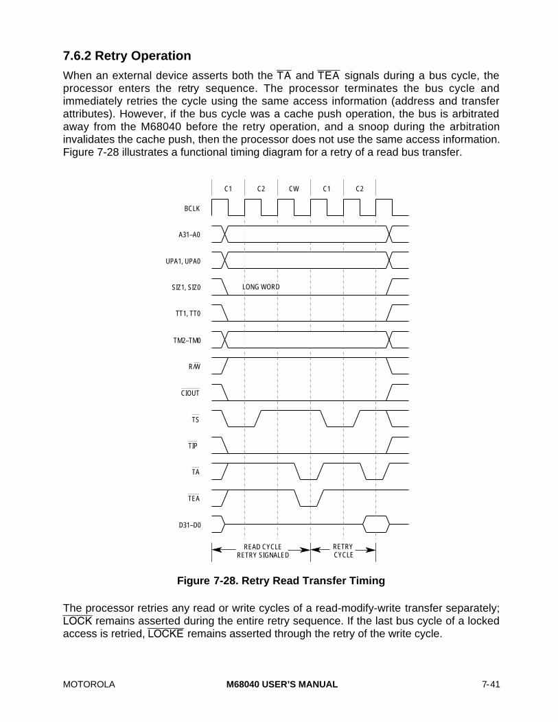
MOTOROLA M68040 USER’S MANUAL 7-41
7.6.2 Retry Operation
When an external device asserts both the TA and TEA signals during a bus cycle, theprocessor enters the retry sequence. The processor terminates the bus cycle andimmediately retries the cycle using the same access information (address and transferattributes). However, if the bus cycle was a cache push operation, the bus is arbitratedaway from the M68040 before the retry operation, and a snoop during the arbitrationinvalidates the cache push, then the processor does not use the same access information.Figure 7-28 illustrates a functional timing diagram for a retry of a read bus transfer.
C1 C2
A31–A0
BCLK
SIZ1, SIZ0
TT1, TT0
TM2–TM0
D31–D0
UPA1, UPA0
CIOUT
TS
TIP
TA
R/W
READ CYCLE RETRY SIGNALED
RETRY CYCLE
C1 C2
TEA
CW
LONG WORD
Figure 7-28. Retry Read Transfer Timing
The processor retries any read or write cycles of a read-modify-write transfer separately;LOCK remains asserted during the entire retry sequence. If the last bus cycle of a lockedaccess is retried, LOCKE remains asserted through the retry of the write cycle.

7-42 M68040 USER’S MANUAL MOTOROLA
On the initial cycle of a line transfer, a retry causes the processor to retry the bus cycle asillustrated in Figure 7-29. However, the processor recognizes a retry signaled during thesecond, third, or fourth cycle of a line as a bus error and causes the processor to abort theline transfer. A burst-inhibited line transfer can only be retried on the initial transfer. Aburst-inhibited line transfer aborts if a retry is signaled for any of the three long-wordtransfers used to complete the line transfer. Negating the bus grant (BG) signal on theM68040 while asserting both TA and TEA provides a relinquish and retry operation for anybus cycle that can be retried (see Figure 7-31).
C1 C2
A31–A0
BCLK
SIZ1, SIZ0
TT1, TT0
TM2–TM0
D31–D0
UPA1, UPA0
CIOUT
TS
TIP
TA
R/W
LINE
RETRY SIGNALED
RETRY CYCLE
C1 C2
TEA
TBI
C3 C4 C5
Figure 7-29. Retry Operation on Line Write

MOTOROLA M68040 USER’S MANUAL 7-43
7.6.3 Double Bus Fault
A double bus fault occurs when an access or address error occurs during the exceptionprocessing sequence—e.g., the processor attempts to stack several words containinginformation about the state of the machine while processing an access error exception. Ifa bus error occurs during the stacking operation, the second error is considered a doublebus fault.
The M68040 indicates a double bus fault condition by continuously driving PST3–PST0with an encoded value of $5 until the processor is reset. Only an external reset operationcan restart a halted processor. While the processor is halted, negating BR and forcing alloutputs to a high-impedance state releases the external bus.
A second access or address error that occurs during execution of an exception handler orlater, does not cause a double bus fault. A bus cycle that is retried does not constitute abus error or contribute to a double bus fault. The processor continues to retry the samebus cycle as long as external hardware requests it.
7.7 BUS SYNCHRONIZATION
The M68040 integer unit generates access requests to the instruction and data memoryunits to support integer and floating-point operations. Both the <ea> fetch and write-backstages of the integer unit pipeline perform accesses to the data memory unit, with effectiveaddress fetches assigned a higher priority. This priority allows data read and writeaccesses to occur out of order, with a memory write access potentially delayed for manyclocks while allowing read accesses generated by later instructions to complete. Theprocessor detects a read access that references earlier data waiting to be written (addresscollisions) and allows the corresponding write access to complete. A given sequence ofread accesses or write accesses is completed in order, and reordering only occurs withwrites relative to reads. Figure 2-1 in Section 2 Integer Unit illustrates the integer pipelinestages.
Besides address collisions, the instruction restart model used for exception processing inthe M68040 causes another potential problem. After the operand fetch for an instruction,an exception that causes the instruction to be aborted can occur, resulting in anotheraccess for the operand after the instruction restarts. For example, an exception couldoccur after a read access of an I/O device’s status register. The exception causes theinstruction to be aborted and the register to be read again. If the first read accesses clearsthe status bits, the status information is lost, and the instruction obtains incorrect data.
Designating the memory page containing the address of the device as serializednoncachable prevents multiple out-of-order accesses to devices sensitive to suchaccesses. When the data memory unit detects an attempt to read an operand from a pagedesignated as serialized noncachable, it allows all pending write accesses to completebefore beginning the external read access. The definition of a page as noncachableversus serialized noncachable only affects read accesses. When a write operationreaches the integer unit’s write-back stage, all previous instructions have completed.When a read access to a serialized noncachable page begins, only a bus error exception

7-44 M68040 USER’S MANUAL MOTOROLA
on the operand read itself can cause the instruction to be aborted, preventing multiplereads. It is important to note that when memory accesses are serialized noncachable,FMOVE will cause two identical writes to the same location to occur if the next instructionprefetch receives a bus error.
Since write cycles can be deferred indefinitely, many subsequent instructions can beexecuted, resulting in seemingly nonsequential instruction execution. When this action isnot desired and the system depends on sequential execution following bus activity, theNOP instruction can be used. The NOP instruction forces instruction and bussynchronization because it freezes instruction execution until all pending bus cycles havecompleted.
A write operation of control information to an external register in which the externalhardware attempts to control program execution based on the data that is written with theconditional assertion of TEA is one situation where the NOP instruction can be used toprevent multiple executions. If the data cache is enabled and the write cycle results in a hitin the data cache, the cache is updated. That data, in turn, may be used in a subsequentinstruction before the external write cycle completes. Since the M68040 cannot processthe bus error until the end of the bus cycle, the external hardware cannot successfullyinterrupt program execution. To prevent a subsequent instruction from executing until theexternal cycle completes, the NOP instruction can be inserted after the instruction causingthe write. In this case, access error exception processing proceeds immediately after thewrite before subsequent instructions are executed. This is an irregular situation, and theuse of the NOP instruction for this purpose is not required by most systems.
Note that the NOP instruction can also be used to force access serialization by placingNOP before the instruction that reads an I/O device. This practice eliminates the need tospecify the entire page as serialized noncachable but does not prevent the instructionfrom being aborted by an exception condition.
7.8 BUS ARBITRATION AND EXAMPLES
The bus design of the M68040 provides for one bus master at a time, either the M68040or an external device. More than one device having the capability to control the bus canbe attached to the bus. An external arbiter prioritizes requests and determines whichdevice is granted access to the bus. Bus arbitration is the protocol by which the processoror an external device becomes the bus master. When the M68040 is the bus master, ituses the bus to read instructions and data not contained in its internal caches frommemory and to write data to memory. When an alternate bus master owns the bus, theM68040 is able to monitor the alternate bus master’s transfer and intervene whennecessary to maintain cache coherency. This capability is discussed in more detail in 7.9Bus Snooping Operation.
Unlike earlier members of the M68000 family, the M68040 implements an arbitrationmethod in which an external arbiter controls bus arbitration and the processor acts as aslave device requesting ownership of the bus from the arbiter. Since the user defines thefunctionality of the external arbiter, it can be configured to support any desired priorityscheme. For systems in which the processor is the only possible bus master, the bus can

MOTOROLA M68040 USER’S MANUAL 7-45
be continuously granted to the processor, and no arbiter is needed. Systems that includeseveral devices that can become bus masters require an arbiter to assign priorities tothese devices so that, when two or more devices simultaneously attempt to become thebus master, the one having the highest priority becomes the bus master first.
7.8.1 Bus Arbitration
The M68040 bus controller generates bus requests to the external arbiter in response tointernal requests from the instruction and data memory units. The M68040 performs busarbitration using the bus request (BR), bus grant (BG), and bus busy (BB) signals. Thearbitration protocol, which allows arbitration to overlap with bus activity, requires a singleidle clock to prevent bus contention when transferring bus ownership between busmasters. The bus arbitration unit in the M68040 operates synchronously and transitionsbetween states on the rising edge of BLCK.
The M68040 requests the bus from the external bus arbiter by asserting BR whenever aninternal bus request is pending. The processor continues to assert BR for as long as itrequires the bus. The processor negates BR at any time without regard to the status of BG
and BB. If the bus is granted to the processor when an internal bus request is generated,BR is asserted simultaneously with transfer start (TS), allowing the access to beginimmediately. The processor always drives BR, and BR cannot be wire-ORed with otherdevices.
The external arbiter asserts BG to indicate to the processor that it has been granted thebus. If BG is negated while a bus cycle is in progress, the processor relinquishes the busat the completion of the bus cycle. To guarantee that the bus is relinquished, BG must benegated prior to the rising edge of the BCLK in which the last TA or TEA is asserted. Notethat the bus controller considers the four bus transfers for a burst-inhibited line transfer tobe a single bus cycle and does not relinquish the bus until completion of the fourthtransfer. The read and write portions of a locked read-modify-write sequence are divisiblein the M68040, allowing the bus to be arbitrated away during the locked sequence. Forsystem applications that do not allow locked sequences to be broken, the arbiter can useLOCK to detect locked accesses and prevent the negation of BG to the processor duringthese sequences. The processor also provides the LOCKE signal to indicate the last writecycle of a locked sequence, allowing arbitration between back-to-back locked sequences.See 7.4.5 Read-Modify-Write Transfers (Locked Transfers) for a detailed description ofread-modify-write transfers.
When the bus has been granted to the processor in response to the assertion of BR, oneof two situations can occur. In the first situation, the processor monitors BB to determinewhen the bus cycle of the alternate bus master is complete. After the alternate bus masternegates BB , the processor asserts BB to indicate explicit bus ownership and begins thebus cycle by asserting TS. The processor continues to assert BB until the external arbiternegates BG, after which BB is first negated at the completion of the bus cycle, then forcedto a high-impedance state. As long as BG is asserted, BB remains asserted to indicate thebus is owned, and the processor continuously drives the bus signals. The processornegates BR when there are no pending accesses to allow the external arbiter to grant thebus to the alternate bus master if necessary.

7-46 M68040 USER’S MANUAL MOTOROLA
In the second situation, the processor samples BB until the external bus arbiter negatesBB. The processor drives its output pins with undetermined values and three-states BB,but does not perform a bus cycle. This procedure, called implicit ownership of the bus,occurs when the processor is granted the bus but there are no pending bus cycles. If aninternal access request is generated, the processor assumes explicit ownership of the busand immediately begins an access, simultaneously asserting BB, BR, TIP, and TS. If theexternal arbiter keeps BG asserted after completion of the bus cycle, the processor keepsBB asserted and drives the bus with undefined values, causing the processor to park. Inthis case, because BB remains asserted until the external arbiter negates BG, theprocessor must assert BR, TIP, and TS simultaneously to enter an active bus cycle. Whenit completes the active bus cycle and the external arbiter has not negated BG, theprocessor goes back into park, negating BR, TIP, and TS. As long as BG is asserted, theprocessor oscillates between park and active bus cycles.
The M68040 can be in any one of five bus arbitration states during bus operation: idle,snoop, implicit ownership, park, and active bus cycle. There are two characteristics thatdetermine these five states: whether the three-state logic determines if the M68040 drivesthe bus and how the M68040 drives BB. If neither the processor nor the external busarbiter asserts BB, then an external pullup resistor drives BB high to negate it. Note thatthe relationship between the internal BR and the external BR is best described as asynchronous delay off BCLK.
The idle state occurs when the M68040 does not have ownership of the bus and is not inthe process of snooping an access. In the idle state, BB is negated and the M68040 doesnot drive the bus. The snoop state is similar to the idle state in that the M68040 does nothave ownership of the bus. The snoop state differs from the idle state in that the M68040is ready to service snooped transfers. Otherwise, the status of BB and the bus is identical.
The implicit ownership state indicates that the M68040 owns the bus. The M68040explicitly owns the bus when it runs a bus cycle immediately after being granted the bus. Ifthe processor has completed at least one bus cycle and no internal transfers are pending,the processor drives the bus with undefined values, entering the park state. In either case,BG remains asserted. The simultaneous assertion of BR, TIP, and TS allows the processorto leave the park state and enter the active bus cycle state.
Figure 7-30 is a bus arbitration state diagram illustrating the relationship of these fivestates with an example of an external bus arbiter circuit. Table 7-6 lists the five states andthe conditions that indicate them.

MOTOROLA M68040 USER’S MANUAL 7-47
OWN/PARK,
IMPLICIT OWNERSHIP,
BGI Λ
*TSI
*BG
I Λ *T
SI Λ
*BBI
*EN
DC
YCLE
Λ *B
BI
*EN
DC
YCLE
Λ B
BI Λ
BG
BG* Λ IBR
SNOOP, BBO DRIVEN BY
MC68040, *THREE-STATED
*BG Λ IBR
ENDCYCLE
*ENDCYCLE Λ BBI Λ *BG Λ IBR *ENDCYCLE Λ BBI Λ *BG Λ *IBR
BG Λ ENDCYCLE Λ *TIP
*BG
BBI Λ *BG Λ IBR Λ TSI
BG
BG Λ TIP
BBI Λ *BG Λ *IBR Λ TSI
BG Λ *ENDCYCLE Λ TIP*
BG Λ TSI*BG Λ TSI Λ *BBI
IDLE,*BG Λ *TSI Λ BBI PROTOCOL
VIOLATION
IBR BBI TSI ENDCYCLE
= Internal bus request signal (see schematic below). = Bus busy driven by alternate bus master.= Transfer start as an input, sampled by the MC68040. = Whatever terminates a bus transaction whether it is normal, bus error, or retried. Note that false burst cycles are treated as a line transaction. False locked transactions are treated the same as any other bus cycle.
*BBO DRIVEN BY MC68040,
THREE-STATED
BBO DRIVEN BY MC68040,
THREE-STATED
BBO DRIVEN BY MC68040,
*THREE-STATED
D
BBBBI
QBR
BBO
IBR
BCLK= The 040 may or may not transition if an active bus cycle is terminated with a bus error, and BG is asserted.
* = Indicates the signal is asserted for that device.
Figure 7-30. M68040 Internal Interpretation State Diagram andExternal Bus Arbiter Circuit
7-48 M68040 USER’S MANUAL MOTOROLA
Table 7-6. M68040 Bus Arbitration States
BB BG State Conditions
Negated Negated Idle M68040 three-states BB; arbiter negatesBG; bus is not driven.
Negated Asserted Implicit Ownership M68040 three-states BB; arbiter assertsBG; bus is driven with undefined values.
Asserted Negated Active Bus CycleM68040 asserts BB; arbiter asserts BG;bus is driven with defined values;TIP is asserted.
Asserted Asserted ParkM68040 asserts BB; arbiter asserts BG;bus is driven with undefined values; TIP isasserted.
Asserted Asserted Alternate Bus Master Ownershipand Snooped
M68040 three-states BB; arbiter assertsBG; M68040 does not drive the bus.
The M68040 can be in the active bus cycle, park, or implicit ownership states when BG isnegated. Depending on the state the processor is in when BG is negated, uncertainconditions can occur. The only guaranteed time that the processor relinquishes the bus iswhen BG is negated prior to the rising edge of BCLK in which the last TA or TEA isasserted and the processor is in the active bus cycle state. However, if the processor is ineither the active bus cycle, park, or implicit ownership states and BG is negated at thesame time or after the last TA or TEA is asserted, then from the standpoint of the externalbus arbiter, the next action that the processor takes is undetermined because theprocessor can internally decide to perform another active bus cycle (indeterminatecondition).
External bus arbiters must consider this indeterminate condition when negating BG andmust be designed to examine the state of BB immediately after negating BG to determinewhether or not the processor will run another bus cycle. A somewhat dangerous situationexists when the processor begins a locked transfer after the bus has been granted to thealternate bus master, causing the alternate bus master to perform a bus transfer during alocked sequence. To correct this situation, the external bus arbiter must be able torecognize the possible indeterminate condition and reassert BG to the processor when theprocessor begins a locked sequence. The indeterminate condition is most significant whendealing with systems that cannot allow locked transfers to be broken. Figure 7-31illustrates an example of an error condition that is a consequence of the interactionbetween the indeterminate condition and a locked transfer. External bus arbiters must bedesigned so that all bus grants to all bus masters be nagated for at least one rising edgeof BCLK between bus tenures; preventing bus conflicts resulting from the aboveconditions.

MOTOROLA M68040 USER’S MANUAL 7-49
040_BG
AM_BG
040_BB
POSSIBLE INDETERMINATE
CONDITION
AM_BB
THE 040 ACTIVELY OWNS THE BUS HERE
040_LOCK
LOCK IS VIOLATED
040_TS
040_TA
AM_TS
*AM indicates the alternate bus master.
*
*
*
Figure 7-31. Lock Violation Example
In addition to the indeterminate condition, the external arbiter’s design needs to includethe function of BR. For example, in certain cases associated with conditional branches,the M68040 can assert BR to request the bus from an alternate bus master, then negateBR without using the bus, regardless of whether or not the external arbiter eventuallyasserts BG. This situation happens when the M68040 attempts to prefetch an instructionfor a conditional branch. To achieve maximum performance, the processor prefetches theinstructions of both paths for a conditional branch. If the conditional branch results in abranch-not-taken, the previously issued branch-taken prefetch is then terminated since theprefetch is no longer needed. In an attempt to save time, the M68040 negates BR. If BG
takes too long to assert, the M68040 enters a disregard request condition.
The BR signal can be reasserted immediately for a different pending bus request, or it canstay negated indefinitely. If an external bus arbiter is designed to wait for the M68040 toassert BB before proceeding, then the system experiences an extended period of time inwhich bus arbitration is locked. Motorola recommends that an external bus arbiter notassume that there is a direct relationship between BR and BB or BR and BG signals.
Figure 7-32 illustrates an example of the processor requesting the bus from the externalbus arbiter. During C1, the M68040 asserts BR to request the bus from the arbiter, whichnegates the alternate bus master’s BG signal and grants the bus to the processor byasserting BG during C3. During C3, the alternate bus master completes its current accessand relinquishes the bus by three-stating all bus signals. Typically, the BB and TIP signals

7-50 M68040 USER’S MANUAL MOTOROLA
require a pullup resistor to maintain a logic-one level between bus master tenures. Thealternate bus master should negate these signals before three-stating to minimize risetime of the signals and ensure that the processor recognizes the correct level on the nextBCLK rising edge. At the end of C3, the processor recognizes the bus grant and bus idleconditions (BG asserted and BB negated) and assumes ownership of the bus by assertingBB and immediately beginning a bus cycle during C4. During C6, the processor begins thesecond bus cycle for the misaligned operand and negates BR since no other accesses arepending. During C7, the external bus arbiter grants the bus back to the alternate busmaster that is waiting for the processor to relinquish the bus. The processor negates BB
and TIP before three-stating these and all other bus signals during C8. Finally, thealternate bus master recognizes the bus grant and idle conditions at the end of C8 and isable to resume bus activity during C9.
A31–A0
BCLK
D31–D0
TRANSFER ATTRIBUTES
TS
TIP
TA
ALTERNATE MASTER
PROCESSOR
BR
BG
BB
AM_BR
AM_BG
ALTERNATE MASTER
C1 C2 C3 C4 C5 C8 C9C6 C7
*
*
*AM indicates the alternate bus master.
Figure 7-32. Processor Bus Request Timing

MOTOROLA M68040 USER’S MANUAL 7-51
Figure 7-33 illustrates a functional timing diagram for an arbitration of a relinquish andretry operation. Figure 7-34 is a functional timing diagram for implicit ownership of the bus.In Figure 7-33, the processor read access that begins in C1 is terminated at the end of C2with a retry request and BG negated, forcing the processor to relinquish the bus and allowthe alternate master to access the bus. Note that the processor reasserts BR during C3since the original access is pending again. After alternate bus master ownership, the busis granted to the processor to allow it to retry the access beginning in C7.
A31–A0
BCLK
D31–D0
TRANSFER ATTRIBUTES
TS
TIP
TA
ALTERNATE MASTER
PROCESSOR
BR
BG
BB
AM_BR
AM_BG
C1 C2 C3 C4 C5 C8C6 C7
TEA
R/W
PROCESSOR
*
*
*AM indicates the alternate bus master.
Figure 7-33. Arbitration During Relinquish and Retry Timing
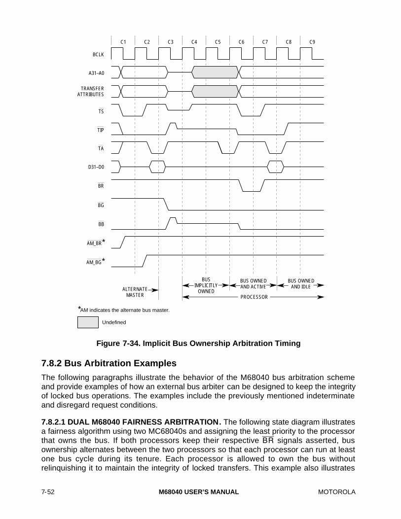
7-52 M68040 USER’S MANUAL MOTOROLA
A31–A0
BCLK
D31–D0
TRANSFER ATTRIBUTES
TS
TIP
TA
ALTERNATE MASTER PROCESSOR
BUS IMPLICITLY
OWNED
BUS OWNED AND ACTIVE
BUS OWNED AND IDLE
BR
BG
BB
AM_BR
AM_BG
C1 C2 C3 C4 C5 C8 C9C6 C7
*
*
*AM indicates the alternate bus master.
Undefined
Figure 7-34. Implicit Bus Ownership Arbitration Timing
7.8.2 Bus Arbitration Examples
The following paragraphs illustrate the behavior of the M68040 bus arbitration schemeand provide examples of how an external bus arbiter can be designed to keep the integrityof locked bus operations. The examples include the previously mentioned indeterminateand disregard request conditions.
7.8.2.1 DUAL M68040 FAIRNESS ARBITRATION. The following state diagram illustratesa fairness algorithm using two MC68040s and assigning the least priority to the processorthat owns the bus. If both processors keep their respective BR signals asserted, busownership alternates between the two processors so that each processor can run at leastone bus cycle during its tenure. Each processor is allowed to own the bus withoutrelinquishing it to maintain the integrity of locked transfers. This example also illustrates
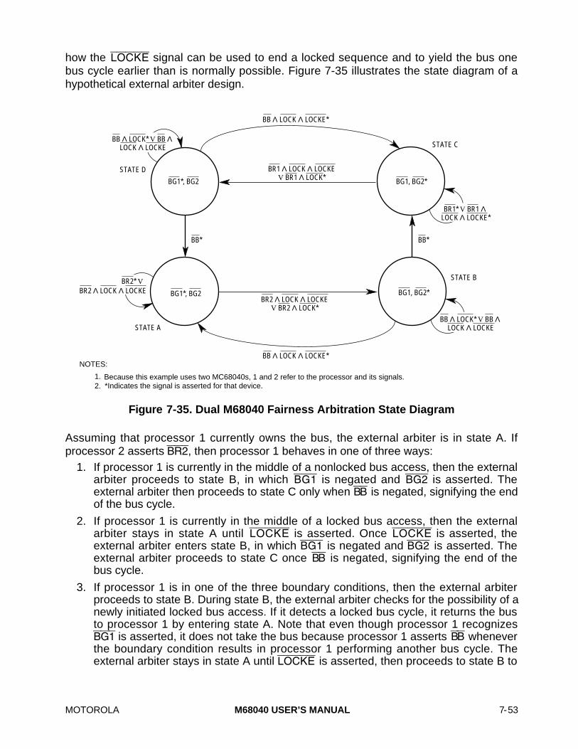
MOTOROLA M68040 USER’S MANUAL 7-53
how the LOCKE signal can be used to end a locked sequence and to yield the bus onebus cycle earlier than is normally possible. Figure 7-35 illustrates the state diagram of ahypothetical external arbiter design.
BB Λ LOCK Λ LOCKE*
STATE A
STATE B
STATE C
STATE D
BR1* V BR1 Λ LOCK Λ LOCKE*
BB Λ LOCK* V BB Λ LOCK Λ LOCKE
BG1*, BG2 BG1, BG2*
BR2 Λ LOCK Λ LOCKE V BR2 Λ LOCK*
BR2* V BR2 Λ LOCK Λ LOCKE
BB*
BG1*, BG2 BG1, BG2*
BB Λ LOCK* V BB Λ LOCK Λ LOCKE
BB*
BR1 Λ LOCK Λ LOCKE V BR1 Λ LOCK*
Because this example uses two MC68040s, 1 and 2 refer to the processor and its signals.*Indicates the signal is asserted for that device.
NOTES:
1. 2.
BB Λ LOCK Λ LOCKE*
Figure 7-35. Dual M68040 Fairness Arbitration State Diagram
Assuming that processor 1 currently owns the bus, the external arbiter is in state A. Ifprocessor 2 asserts BR2, then processor 1 behaves in one of three ways:
1. If processor 1 is currently in the middle of a nonlocked bus access, then the externalarbiter proceeds to state B, in which BG1 is negated and BG2 is asserted. Theexternal arbiter then proceeds to state C only when BB is negated, signifying the endof the bus cycle.
2. If processor 1 is currently in the middle of a locked bus access, then the externalarbiter stays in state A until LOCKE is asserted. Once LOCKE is asserted, theexternal arbiter enters state B, in which BG1 is negated and BG2 is asserted. Theexternal arbiter proceeds to state C once BB is negated, signifying the end of thebus cycle.
3. If processor 1 is in one of the three boundary conditions, then the external arbiterproceeds to state B. During state B, the external arbiter checks for the possibility of anewly initiated locked bus access. If it detects a locked bus cycle, it returns the busto processor 1 by entering state A. Note that even though processor 1 recognizesBG1 is asserted, it does not take the bus because processor 1 asserts BB wheneverthe boundary condition results in processor 1 performing another bus cycle. Theexternal arbiter stays in state A until LOCKE is asserted, then proceeds to state B to

7-54 M68040 USER’S MANUAL MOTOROLA
give the bus to processor 2. The arbiter remains in state B until BB is negated,signifying the end of the bus cycle.
Once state C is reached, depending on whether or not processor 2 asserts BR2 and thennegates BR2 because of a disregard request condition, processor 1 may or may notactively begin a bus cycle. If no other bus requests are pending by the time state C isreached, processor 2 is in the implicit ownership state. If processor 1 asserts BR1, then itis possible for state C to persist for only one clock. In this case, processor 2 does not havea chance to run any active bus cycles.
A null bus cycle tenure is better than having the external bus arbiter wait for processor 2 toperform at least one bus cycle before returning bus ownership to processor 1, eventhough this appears to be a waste of bus arbitration overhead. Note that once processor 2enters the disregard request condition, processor 2 reasserts BR anywhere from one clockto an undetermined number of clocks before running another bus cycle. Waiting forprocessor 2 to run a bus cycle can result in a temporary bus arbitration lockup.
This bus arbitration scheme is restricted if the system supports the relinquish and retryoperation that can occur for the last write cycle of a locked transfer. In this case, LOCKE
cannot be used. Assuming that LOCKE is always negated excludes the need for LOCKE inan arbitration similar to this example. The reason for this restriction is that the external busarbiter gives up the bus to the other processor once LOCKE is asserted. If a relinquish andretry operation were to occur, then the next bus cycle would be from the other processorviolating the integrity of the locked transfer.
7.8.2.2 DUAL M68040 PRIORITIZED ARBITRATION. This example is very similar to thedual M68040 fairness arbitration example, except that one processor is assigned higherpriority over the other. Processor 2 can own the bus only if there are no processor 1pending requests. It is important to note that when the processor asserts the LOCK signal,it also asserts BR1. This implementation replaces LOCK with BR because BR is moredemanding than using LOCK. Only when processor 2 is in the middle of a lockedoperation does it have higher priority than processor 1. Similar to the M68040 fairnessarbitration example, the restriction on using LOCKE applies to this example. Figure 7-36illustrates the state diagram for dual M68040 prioritized arbitration.

MOTOROLA M68040 USER’S MANUAL 7-55
BB Λ LOCK Λ LOCKE*
BR1 Λ BR2*
BB Λ BR2
STATE A
STATE B
STATE C
STATE D
BB Λ BR2*
BR2 V BR1*Λ BR2*
BB Λ LOCK* V BB & LOCK Λ LOCKE
BG1*, BG2 BG1, BG2*
BR2 Λ LOCK Λ LOCKE V BR2 Λ LOCK*
BR2* V BR2 Λ LOCK Λ LOCKE* BG1*, BG2 BG1, BG2*
Because this example uses two MC68040s, 1 or 2 refers to the processor and its signals.*Indicates the signal is asserted for that device.
NOTES:
1. 2.
BB* BB*
Figure 7-36. Dual M68040 Prioritized Arbitration State Diagram
7.8.2.3 M68040 SYNCHRONOUS DMA ARBITRATION. Figure 7-37 illustrates a systemwith an M68040 and a synchronous direct memory access (DMA) that contains anM68040 interface. Figure 7-37(a) illustrates that the DMA owning the bus only when theM68040 has no pending requests, and Figure 7-37(b) illustrates the DMA having higherpriority than the M68040 causing the M68040 to yield the bus to the DMA at any timeexcept when the M68040 is performing a locked bus operation. In either case, the M68040is the default bus master; if there are no pending requests from either device, the externalarbiter gives the bus to the M68040. Similar to the M68040 fairness arbitration example,the restriction on using LOCKE applies to this example.

7-56 M68040 USER’S MANUAL MOTOROLA
040_BR
STATE A
STATE B
STATE C
STATE D
BB
BB Λ 040_BR*
AM_BG, 040_BG*
040_BR V AM_BR*
(a) MC68040 High Priorty, Default Bus Master
AM_BG, 040_BG* AM_BG*, 040_BG
AM_BG*, 040_BG
040_BR
AM_BR, 040_BG*
BB Λ 040_BR
040_BR*
STATE A
STATE B
STATE C
STATE D
BB Λ AM_BR*
BB Λ LOCK* V BB Λ LOCK Λ LOCKE
AM_BG, 040_BG*
AM_BR* V AM_BR Λ LOCK Λ LOCKE*
(b) MC68040 Low-Priorty, Default Bus Master
AM_BG, 040_BG* AM_BG*, 040_BG
AM_BG*, 040_BG
040_BR
BB Λ LOCK Λ LOCKE*
BB Λ AM_BR
AM_BR Λ LOCK Λ LOCKE V AM_BR Λ LOCK*
* Indicates the signal is asserted for that device.
BB* BB*
BB* BB*
Figure 7-37. M68040 Synchronous DMA Arbitration
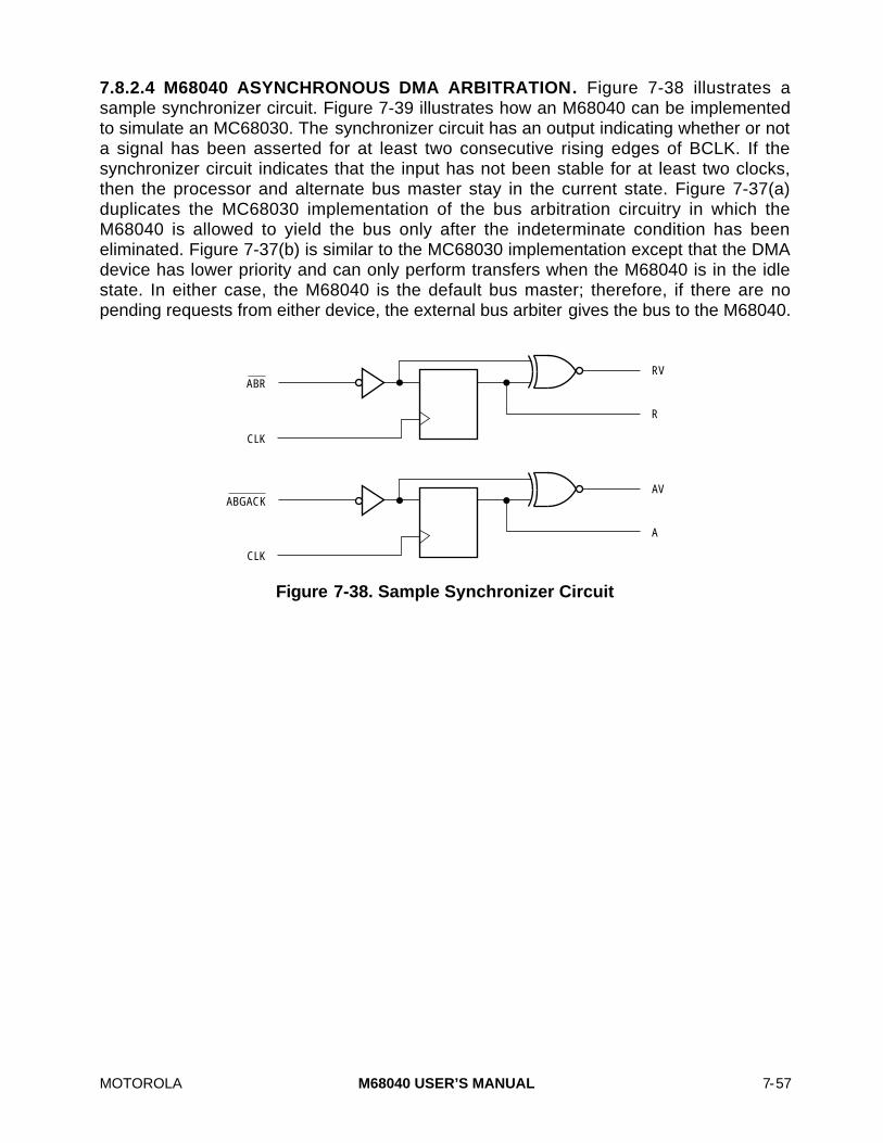
MOTOROLA M68040 USER’S MANUAL 7-57
7.8.2.4 M68040 ASYNCHRONOUS DMA ARBITRATION. Figure 7-38 illustrates asample synchronizer circuit. Figure 7-39 illustrates how an M68040 can be implementedto simulate an MC68030. The synchronizer circuit has an output indicating whether or nota signal has been asserted for at least two consecutive rising edges of BCLK. If thesynchronizer circuit indicates that the input has not been stable for at least two clocks,then the processor and alternate bus master stay in the current state. Figure 7-37(a)duplicates the MC68030 implementation of the bus arbitration circuitry in which theM68040 is allowed to yield the bus only after the indeterminate condition has beeneliminated. Figure 7-37(b) is similar to the MC68030 implementation except that the DMAdevice has lower priority and can only perform transfers when the M68040 is in the idlestate. In either case, the M68040 is the default bus master; therefore, if there are nopending requests from either device, the external bus arbiter gives the bus to the M68040.
ABR
CLK
RV
R
ABGACK
CLK
AV
A
Figure 7-38. Sample Synchronizer Circuit

7-58 M68040 USER’S MANUAL MOTOROLA
AM_BG*, 040_BG
040_BG*, AM_BG*
R Λ RV Λ A* Λ AV V AV* V RV*
R* V RV* V R Λ RV Λ LOCK Λ
LOCKE*
R Λ RV Λ LOCK Λ LOCKE V R Λ RV Λ
LOCK*
LOCK Λ LOCKE*
LOCKE V LOCK*
R* Λ RV Λ A* Λ AV V A Λ AV
S1
S2S3
S4
S5
S6
R* Λ RV Λ A Λ AV V RV* V RA*
R* Λ RV Λ A* Λ AV
R Λ RV
RV* V RA* V R Λ RV Λ A Λ AV
R Λ RV Λ A* Λ AVR* Λ RV
(a) MC68040 Low-Priorty, Default Bus Master
040_BG*, AM_BG
040_BG*, AM_BG
040_BG*, AM_BG*
040_BG*, AM_BG*
040_BG*, AM_BG
040_BG*, AM_BG
AM_BG*, 040_BG
040_BG*, AM_BG*
R* Λ RV Λ A* Λ AV V R Λ RV Λ 040_BR
R* V RV* V 040_BR
R Λ RV Λ 040_BR
040_BRR* Λ RV Λ A* Λ AV
V A Λ AV
S1
S2S3
S4
S5
S6
R Λ RV Λ 040_BR
R Λ RV Λ A* Λ AVR* Λ RV
1. It is assumed that the asynchronous device takes the bus only after TIP or the MC68040's BB is negated.
040_BG*, AM_BG
040_BG*, AM_BG
040_BG*, AM_BG*
040_BG*, AM_BG*
040_BG*, AM_BG
040_BG*, AM_BG
040_BR
R* Λ RV Λ A* Λ AV V AV* V RV*
(b) MC68040 High-Priorty, Default Bus Master
RV* V RA* V R Λ RV Λ A Λ AV
R* Λ RV Λ A Λ AV V RV* V RA*
NOTES:
2. *Indicates the signal is asserted for that device.
Figure 7-39. M68040 Asynchronous DMA Arbitration
MOTOROLA M68040 USER’S MANUAL 7-59
7.9 BUS SNOOPING OPERATION
When required, the M68040 can monitor alternate bus master transfers and intervene inthe access to maintain cache coherency. The encoding of the SCx signals generated bythe alternate bus master for each bus cycle controls the process of bus monitoring andintervention called snooping. Only byte, word, long-word, and line bus transfers can besnooped. Refer to Section 4 Instruction and Data Caches for SCx encodings.
When the M68040 recognizes that an alternate bus master has asserted T S, theprocessor latches the level on the byte offset, SIZx, TMx, and R/W signals during therising edge of BCLK for which TS is first asserted. The processor then evaluates the SCxand TTx signals to determine the type of access (TTx = $0 or $1), if it is snoopable, and, ifso, how it should be snooped. If snooping is enabled for the access, the processor inhibitsmemory from responding by continuing to assert the memory inhibit signal (MI) whilechecking the internal caches for matching lines. During the snooped bus cycle, theM68040 ignores all TA assertions while MI is asserted. Unless the data cache contains adirty line corresponding to the access and the requested snoop operation indicates sinkdata for a write or source data for a read, MI is negated, and memory is allowed torespond and complete the access. Otherwise, the processor continues to intervene in theaccess by keeping MI asserted and responding to the alternate bus master as a slavedevice. The processor monitors the levels of TA, TEA, and TBI to detect normal, bus error,retry, and burst-inhibited terminations. Note that for alternate bus master burst-inhibitedline transfers, the M68040 snoops each of the four resulting long-word transfers. Ifsnooping is disabled, MI is negated, and the M68040 counts the appropriate number of TA
or TEA assertions before proceeding. For example, if the SIZx signals are pulled high, theM68040 requires four TA assertions, one TEA assertion, or one retry termination beforeproceeding.
As a bus master, the M68040 can be configured to request snooping operations on apage-by-page basis. The UPAx signals are connected to the SCx inputs of the snoopingprocessors. Appropriately programming the user attribute bits in the corresponding pagedescriptor selects the required snooping operation for a page. Refer to Section 3 MemoryManagement Unit (Except MC68EC040 and MC68EC040V) for details on configuringthe caching mode and user attribute bits for each memory page for the M68040 andMC68LC040, and refer to Appendix B MC68EC040 for the MC68EC040.
In a system with multiple bus masters, the memory unit must wait for each snooping busmaster to negate MI before responding to an access. A termination signal asserted beforethe negation of MI leads to undefined operation and must be avoided at all costs. Also, ifthe system contains multiple caching masters, then each master must access shared datausing write-through pages that allow writes to the data to be snooped by other masters.The copyback caching mode is typically used for data local to a processor because in amultimaster caching system only one master at a time can access a given page ofcopyback data. The copyback caching mode also prevents multiple snooping processorsfrom intervening in a specific access.

7-60 M68040 USER’S MANUAL MOTOROLA
7.9.1 Snoop-Inhibited Cycle
For alternate bus master accesses in which the SCx signal encodings indicate thatsnooping is inhibited (SCx = $0), the M68040 immediately negates MI and allows memoryto respond to the access. Snoop-inhibited alternate bus master accesses do not affectperformance of the processor since no cache lookups are required. Figure 7-40 illustratesan example of a snoop-inhibited operation in which an alternate bus master is granted thebus for an access. No matter what the values are on the SCx and TTx signals, MI isasserted between bus cycles. Because MI is asserted while a cache lookup is performed,snooping inherently degrades system performance.
MI is asserted from the last TA of the current bus cycle if the M68040 owns the bus andloses it (see Figure 7-40). If an alternate bus master has the bus and loses it, there aretwo different resulting cases. Usually, an idle clock occurs between the alternate busmaster’s cycle and the MC68040’s cycle. If so, MI is asserted during the idle clock andnegated from the same edge that the M68040 asserts the TS signal (see Figure 7-40). Ifthere is no idle clock, MI is not asserted. MI is asserted during and after reset until the firstbus cycle of the M68040. Even though snoop is inhibited, all TA or TEA assertions whileMI is asserted are ignored. If a line snoop is started, the M68040 still requires four TA
assertions.

MOTOROLA M68040 USER’S MANUAL 7-61
A31–A0
BCLK
D31–D0
TS
TA
ALTERNATE MASTERPROCESSOR
BR
BG
BB
AM_BR
AM_BG
PROCESSOR
SC1, SC0
SIZ1, SIZ0
TT1, TT0
R/W
MI
C1 C2 C3 C1 C2 C3
Undefined
*
*
*AM indicates the alternate bus master.
Figure 7-40. Snoop-Inhibited Bus Cycle
7.9.2 Snoop-Enabled Cycle (No Intervention Required)
For alternate bus master accesses in which SCx = $1 or $2, indicating that snooping isenabled, the M68040 continues to assert MI while checking for a matching cache line. Ifintervention in the alternate bus master access is not required, MI is then negated, andmemory is allowed to respond and complete the access. Figure 7-41 illustrates anexample of snooping in which memory is allowed to respond. Best-case timing is

7-62 M68040 USER’S MANUAL MOTOROLA
illustrated, which results in a memory access having the equivalent of two wait states.Variations in the timing required by snooping logic to access the caches can delay thenegation of MI by up to two additional clocks. External logic must ensure that thetermination signals negate at all rising BCLK edges in which MI is asserted. Otherwise, ifone of the termination signals is asserted, either the M68040 ignores all terminationsignals, reading them as negated, or the M68040 exhibits improper operation.
A31–A0
BCLK
D31–D0
TS
TA
ALTERNATE MASTER
BR
BG
BB
AM_BR
AM_BG
PROCESSOR
SC1–SC0
SIZ1, SIZ0
TT1, TT0
R/W
MI
C1 C2 C3 C4 C5 C6
Undefined
*
*AM indicates the alternate bus master.
*
Figure 7-41. Snoop Access with Memory Response
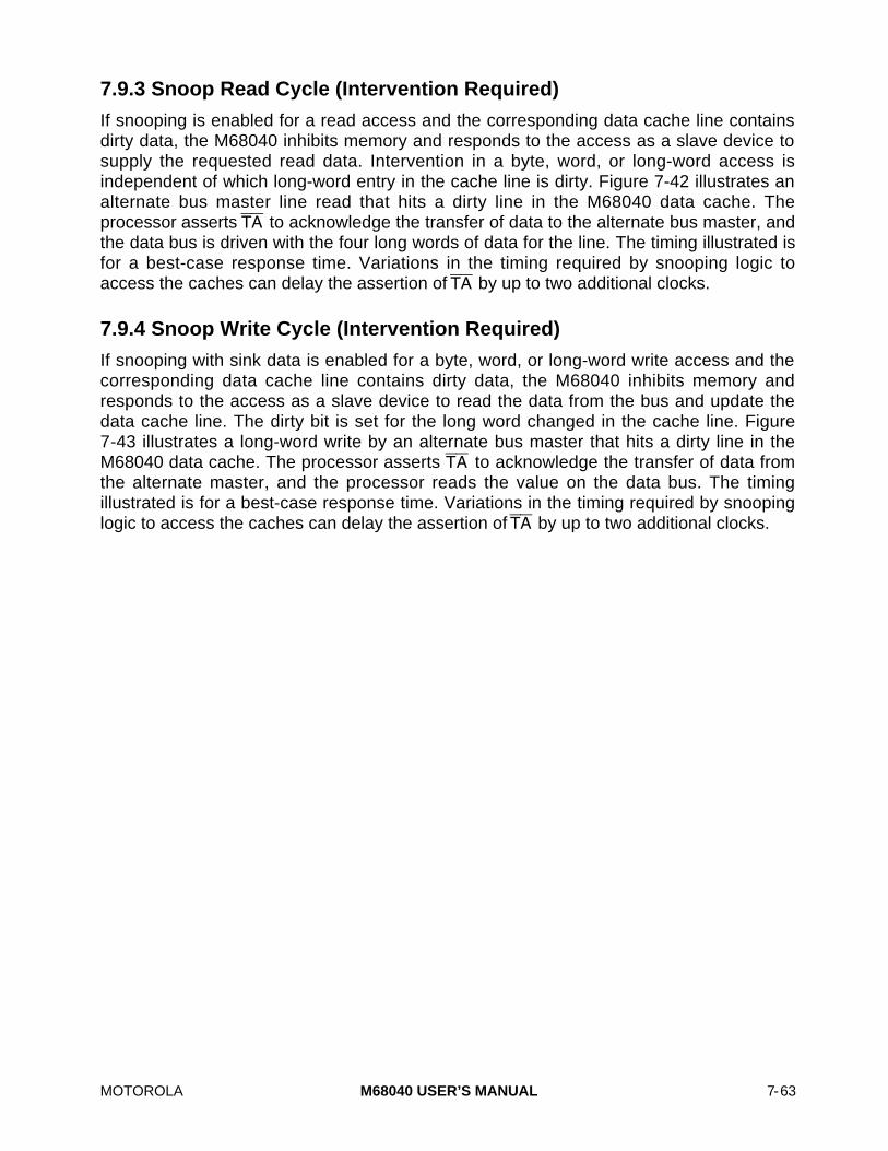
MOTOROLA M68040 USER’S MANUAL 7-63
7.9.3 Snoop Read Cycle (Intervention Required)
If snooping is enabled for a read access and the corresponding data cache line containsdirty data, the M68040 inhibits memory and responds to the access as a slave device tosupply the requested read data. Intervention in a byte, word, or long-word access isindependent of which long-word entry in the cache line is dirty. Figure 7-42 illustrates analternate bus master line read that hits a dirty line in the M68040 data cache. Theprocessor asserts TA to acknowledge the transfer of data to the alternate bus master, andthe data bus is driven with the four long words of data for the line. The timing illustrated isfor a best-case response time. Variations in the timing required by snooping logic toaccess the caches can delay the assertion of TA by up to two additional clocks.
7.9.4 Snoop Write Cycle (Intervention Required)
If snooping with sink data is enabled for a byte, word, or long-word write access and thecorresponding data cache line contains dirty data, the M68040 inhibits memory andresponds to the access as a slave device to read the data from the bus and update thedata cache line. The dirty bit is set for the long word changed in the cache line. Figure7-43 illustrates a long-word write by an alternate bus master that hits a dirty line in theM68040 data cache. The processor asserts TA to acknowledge the transfer of data fromthe alternate master, and the processor reads the value on the data bus. The timingillustrated is for a best-case response time. Variations in the timing required by snoopinglogic to access the caches can delay the assertion of TA by up to two additional clocks.
7-64 M68040 USER’S MANUAL MOTOROLA
A31–A0
BCLK
D31–D0
TS
TA
ALTERNATE MASTER LINE READ
BR
BG
BB
AM_BR
AM_BG
PROCESSOR
SC1, SC0
SIZ1, SIZ0
TT1, TT0
R/W
MI
C1 C2 C3 C4 C5 C6 C7 C8 C9
TA AND DATA DRIVEN BY PROCESSOR
MEMORY INHIBITED FROM RESPONDING
*
*
*AM indicates the alternate bus master.
Figure 7-42. Snooped Line Read, Memory Inhibited

MOTOROLA M68040 USER’S MANUAL 7-65
A31–A0
BCLK
D31–D0
TS
TA
ALTERNATE MASTER LONG-WORD WRITE
BR
BG
BB
PROCESSOR
SC1, SC0
SIZ1, SIZ0
TT1, TT0
R/W
MI
C1 C2 C3 C4 C5 C6
TA DRIVEN BY PROCESSOR
MEMORY INHIBITED FROM RESPONDING
DATA WRITTEN BY ALTERNATE BUS MASTER
AM_BR
AM_BG
*
*
*AM indicates the alternate bus master.
Figure 7-43. Snooped Long-Word Write, Memory Inhibited
7.10 RESET OPERATION
An external device asserts the reset input signal (RSTI) to reset the processor. Whenpower is applied to the system, external circuitry should assert RSTI for a minimum of 10BCLK cycles after VCC is within tolerance. Figure 7-44 is a functional timing diagram ofthe power-on reset operation, illustrating the relationships among VCC, RSTI, modeselects, and bus signals. The BCLK and PCLK clock signals are required to be stable bythe time VCC reaches the minimum operating specification. The VIH levels of the clocks

7-66 M68040 USER’S MANUAL MOTOROLA
should not exceed VCC while it is ramping up. RSTI is internally synchronized for twoBCLKS before being used and must meet the specified setup and hold times to BCLK(specifications #51 and #52 in Section 11 MC68040 Electrical and ThermalCharacteristics) only if recognition by a specific BCLK rising edge is required. MI isasserted while the M68040 is in reset.
BCLK
BUS SIGNALS
+5 V
0 V
RSTI
TS
BR
CDIS, MDIS,IPL2–IPL0
BG
BB
TIP
VCC
Undefined
t 10 CLOCKS
2 CLOCKS
128 CLOCKS
>
MI
Figure 7-44. Initial Power-On Reset Timing
Once RSTI negates, the processor is internally held in reset for another 128 clock cycles.During the reset period, all signals that can be, are three-stated, and the rest are driven totheir inactive state. Once the internal reset signal negates, all bus signals continue toremain in a high-impedance state until the processor is granted the bus. Afterwards, thefirst bus cycle for reset exception processing begins. In Figure 7-44 the processorassumes implicit bus ownership before the first bus cycle begins. The levels on CDIS,MDIS, and IPL2–IPL0 are used to selectively enable the special modes of operation whenRSTI is negated. These signals should be driven to their normal levels before the end ofthe 128-clock internal reset period.

MOTOROLA M68040 USER’S MANUAL 7-67
For processor resets after the initial power-on reset, RSTI should be asserted for at least10 clock periods. Figure 7-45 illustrates timings associated with a reset when theprocessor is executing bus cycles. Note that BB and TIP (and TA if driven during asnooped access) are negated before transitioning to a three-state level.
BCLK
BUS SIGNALS
RSTI
TS
BR
CDIS, MDIS,IPL2–IPL0
BG
BB
TIP
t 10 CLOCKS
2 CLOCKS
128 CLOCKS
>
MI
Figure 7-45. Normal Reset Timing
Resetting the processor causes any bus cycle in progress to terminate as if TA or TEA
had been asserted. In addition, the processor initializes registers appropriately for a resetexception. Section 8 Exception Processing describes exception processing. When aRESET instruction is executed, the processor drives the reset out (RSTO) signal for 512BCLK cycles. In this case, the processor resets the external devices of the system, andthe internal registers of the processor are unaffected. The external devices connected tothe RSTO signal are reset at the completion of the RESET instruction. An RSTI signal thatis asserted to the processor during execution of a RESET instruction immediately resetsthe processor and causes the RSTO signal to negate. RSTO can be logically ANDed withthe external signal driving RSTI to derive a system reset signal that is asserted for both anexternal processor reset and execution of a RESET instruction.
7-68 M68040 USER’S MANUAL MOTOROLA
7.11 SPECIAL MODES OF OPERATION
The MC68LC040 and MC68EC040 do not support the following three modes of operation,which for the M68040 are selectively enabled during processor reset and remain in effectuntil the next processor reset. Refer to Appendix A MC68LC040 and Appendix BMC68EC040 for differences in the special modes of operation for the MC68LC040 andMC68EC040.
7.11.1 Output Buffer Impedance Selection
All output drivers in the M68040 can be configured to operate in either a large buffer mode(low-impedance driver) or small buffer mode (high-impedance driver). Large buffers havea nominal output impedance of 6 Ω for both high and low drive, resulting in minimumoutput delays. Signal traces driven by large buffers usually require transmission lineeffects to be considered in their design, including the use of signal termination. Smallbuffers have a nominal impedance of 25 Ω for high and low drive, resulting in longeroutput delays and less critical board-design requirements. Refer to Section 11 MC68040Electrical and Thermal Characteristics for further information on electricalspecifications, buffer characteristics, and transmission line design examples. The outputdrivers are configured in three groups. Each group of signals is configured depending onthe corresponding IPL≈ signal level during processor reset (see Table 5-5).
7.11.2 Multiplexed Bus Mode
The multiplexed bus mode changes the timing of the three-state control logic for theaddress and data buses to support generation of a multiplexed address/data bus. Whenthe M68040 is operating in this mode, the address and data bus signals can be hardwiredtogether to form a single 32-bit bus, with address and data information time-multiplexed onthe bus. This configuration minimizes the number of pins required to interface toperipheral devices without requiring additional discrete multiplexing logic. This mode isenabled during a processor reset by a logic zero on the CDIS signal.
Figure 7-46 illustrates a line write with multiplexed bus mode enabled. The address busdrivers are enabled during C1 and disabled during C2. Later in C2, the data bus driversare enabled to drive the data bus with the data to be written. The address bus is onlydriven for the BCLK rising edge at the start of each bus cycle.
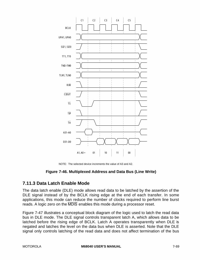
MOTOROLA M68040 USER’S MANUAL 7-69
BCLK
SIZ1, SIZ0
TT1, TT0
TM2–TM0
D31–D0
UPA1, UPA0
CIOUT
TS
TIP
TA
R/W
C1 C2 C3 C4 C5
A31–A0
TLN1, TLN0
NOTE: The selected device increments the value of A3 and A2.
10 11 0001A1, A0 =
Figure 7-46. Multiplexed Address and Data Bus (Line Write)
7.11.3 Data Latch Enable Mode
The data latch enable (DLE) mode allows read data to be latched by the assertion of theDLE signal instead of by the BCLK rising edge at the end of each transfer. In someapplications, this mode can reduce the number of clocks required to perform line burstreads. A logic zero on the MDIS enables this mode during a processor reset.
Figure 7-47 illustrates a conceptual block diagram of the logic used to latch the read databus in DLE mode. The DLE signal controls transparent latch A, which allows data to belatched before the rising edge of BCLK. Latch A operates transparently when DLE isnegated and latches the level on the data bus when DLE is asserted. Note that the DLEsignal only controls latching of the read data and does not affect termination of the bus

7-70 M68040 USER’S MANUAL MOTOROLA
transfer. Edge-triggered latch B is clocked by the rising edge of BCLK and latches thedata from latch A for use by internal logic.
D Q D Q
G
TRANSPARENT LATCH - A
EDGE-TRIGGERED LATCH - B
DLE BCLK
TA, TEA, TBITERMINATION CONTROL
LATCHED READ DATA
WRITE DATA
EXTERNAL DATA BUS
Figure 7-47. DLE Mode Block Diagram
Figure 7-48 illustrates the data read timing for both normal operation and DLE mode.During normal operation (i.e., DLE mode disabled), latch A is always transparent, and bythe rising edge of BCLK, read data is latched. Data must meet setup and hold timespecifications #15 and #16 in this case. When the DLE mode is enabled, the data can belatched by the rising edge of BCLK or the falling edge of DLE, depending on the timing forDLE.

MOTOROLA M68040 USER’S MANUAL 7-71
36
BCLK
D0–D31 IN (READ)
DLE
TA
DLE MODE DATA BUS TIMING
BCLK
D0–D31 IN (READ)
TA
15
16
NORMAL DATA BUS TIMING
CASE 1 CASE 2
3233
3431
3637
35
Figure 7-48. DLE versus Normal Data Read Timing
Case 1If DLE is negated and meets setup time specification #35 to the rising edge of BCLKwhen the bus read is terminated, latch A is transparent, and the read data must meetsetup and hold time specifications #36 and #37 to the rising edge of BCLK. Read timingis similar to normal timing for this case.
Case 2If DLE is asserted, the data bus levels are latched and held internally. D31–D0 mustmeet setup and hold time specifications #32 and #33 to the falling edge of DLE, and cantransition to a new level once DLE is asserted. D31–D0 must still meet setup timespecification #36 to BCLK, but not hold time specification #37, since the data isinternally held valid as long as DLE remains asserted low.

7-72 M68040 USER’S MANUAL MOTOROLA

MOTOROLA M68040 USER’S MANUAL 8-1
SECTION 8EXCEPTION PROCESSING
Exception processing is the activity performed by the processor in preparing to execute aspecial routine for any condition that causes an exception. In particular, exceptionprocessing does not include execution of the routine itself. This section describes theprocessing for each type of integer unit exception, exception priorities, the return from anexception, and bus fault recovery. This section also describes the formats of the exceptionstack frames. For details on floating-point exceptions refer to Section 9 Floating-PointUnit (MC68040 Only).
NOTE
For the MC68040V, MC68LC040, MC68EC040, andMC68EC040V ignore all references to floating-point, includingany instructions that begin with an “F”. Also, for theMC68EC040 and MC68EC040V ignore all references to thememory management unit (MMU) and the instructionsPFLUSH and PTEST. The functionality of the MC68040transparent translation register has been changed in theMC68EC040 and MC68EC040V to the access control registers(ACR). Refer to Appendix A MC68LC040 and Appendix BMC68EC040 for details.
8.1 EXCEPTION PROCESSING OVERVIEW
Exception processing is the transition from the normal processing of a program to theprocessing required for any special internal or external condition that preempts normalprocessing. External conditions that cause exceptions are interrupts from externaldevices, bus errors, and resets. Internal conditions that cause exceptions are instructions,address errors, and tracing. For example, the TRAP, TRAPcc, FTRAPcc, CHK, RTE, DIV,and FDIV instructions can generate exceptions as part of their normal execution. Inaddition, illegal instructions, unimplemented floating-point instructions and data types, andprivilege violations cause exceptions. Exception processing uses an exception vectortable and an exception stack frame. The following paragraphs describe the vector tableand a generalized exception stack frame.
The M68040 uses a restart exception processing model to minimize interrupt andinstruction latency and to reduce the size of the stack frame (compared to the framerequired for a continuation model). Exceptions are recognized at each instructionboundary in the execute stage of the integer pipeline and force later instructions that havenot yet reached the execute stage to be aborted. Instructions that cannot be interrupted,

8-2 M68040 USER’S MANUAL MOTOROLA
such as those that generate locked bus transfers or access serialized pages, are allowedto complete before exception processing begins.
Exception processing occurs in four functional steps. However, all individual bus cyclesassociated with exception processing (vector acquisition, stacking, etc.) are notguaranteed to occur in the order in which they are described in this section. Figure 8-1illustrates a general flowchart for the steps taken by the processor during exceptionprocessing.
During the first step, the processor makes an internal copy of the status register (SR).Then the processor changes to the supervisor mode by setting the S-bit and inhibitstracing of the exception handler by clearing the trace enable (T1 and T0) bits in the SR.For the reset and interrupt exceptions, the processor also updates the interrupt prioritymask in the SR.
During the second step, the processor determines the vector number for the exception.For interrupts, the processor performs an interrupt acknowledge bus cycle to obtain thevector number. For all other exceptions, internal logic provides the vector number. Thisvector number is used in the last step to calculate the address of the exception vector.Throughout this section, vector numbers are given in decimal notation.

MOTOROLA M68040 USER’S MANUAL 8-3
EXIT
FETCH VECTOR NUMBER
(DOUBLE BUS FAULT)
EXECUTE EXCEPTION HANDLER
EXIT
(DOUBLE BUS FAULT)
(DOUBLE BUS FAULT)
ENTRY
SAVE CONTENTS TO STACK FRAME
(SEE NOTE)
PREFETCH 4 LONG WORDS
OTHERWISE BEGIN INSTRUCTION
EXECUTION
OTHERWISEBUS ERROR
BUS ERROR
BUS ERROR OR ADDRESS ERROR
HALTED STATE (PST3–PST0 = $5)
OTHERWISE
SAVE INTERNAL COPY OF SR
S 1 T1, T0 0
(SEE NOTE)
NOTE: These blocks vary for reset and interrupt exceptions.
Figure 8-1. General Exception Processing Flowchart

8-4 M68040 USER’S MANUAL MOTOROLA
The third step is to save the current processor contents for all exceptions other than reset.The processor creates one of five exception stack frame formats on the active supervisorstack and fills it with information appropriate for the type of exception. Other informationcan also be stacked, depending on which exception is being processed and the state ofthe processor prior to the exception. If the exception is an interrupt and the M-bit of theSR is set, the processor clears the M-bit and builds a second stack frame on the interruptstack. Figure 8-2 illustrates the general form of the exception stack frame.
STATUS REGISTER
PROGRAM COUNTER
FORMAT VECTOR OFFSET
ADDITIONAL PROCESSOR STATE INFORMATION (2 OR 26 WORDS, IF NEEDED)
15 12 0
SP
Figure 8-2. General Form of Exception Stack Frame
The last step initiates execution of the exception handler. The processor multiplies thevector number by four to determine the exception vector offset. It adds the offset to thevalue stored in the vector base register (VBR) to obtain the memory address of theexception vector. Next, the processor loads the program counter (PC) (and the interruptstack pointer (ISP) for the reset exception) from the exception vector table entry. Afterprefetching the first four long words to fill the instruction pipe, the processor resumesnormal processing at the address in the PC. When the processor executes an RTEinstruction, it examines the stack frame on top of the active supervisor stack to determineif it is a valid frame and what type of context restoration it requires.
All exception vectors are located in the supervisor address space and are accessed usingdata references. Only the initial reset vector is fixed in the processor’s memory map; onceinitialization is complete, there are no fixed assignments. Since the VBR provides the baseaddress of the exception vector table, the exception vector table can be located anywherein memory; it can even be dynamically relocated for each task that an operating systemexecutes.
The M68040 supports a 1024-byte vector table containing 256 exception vectors (seeTable 8-1). Motorola defines the first 64 vectors and reserves the other 192 vectors foruser-defined interrupt vectors. External devices can use vectors reserved for internalpurposes at the discretion of the system designer. External devices can also supply vectornumbers for some exceptions. External devices that cannot supply vector numbers usethe autovector capability, which allows the M68040 to automatically generate a vectornumber.

MOTOROLA M68040 USER’S MANUAL 8-5
Table 8-1. Exception Vector Assignments
VectorNumber(s)
Vector Offset(Hex) Assignment
0123
00000400800C
Reset Initial Interrupt Stack PointerReset Initial Program CounterAccess FaultAddress Error
4567
01001401801C
Illegal InstructionInteger Divide by ZeroCHK, CHK2 InstructionFTRAPcc, TRAPcc, TRAPV Instructions
891011
02002402802C
Privilege ViolationTraceLine 1010 Emulator (Unimplemented A-Line Opcode)Line 1111 Emulator (Unimplemented F-Line Opcode)
12131415
03003403803C
(Unassigned, Reserved)Defined for MC68020 and MC68030, not used by M68040Format ErrorUninitialized Interrupt
16–23 040–05C (Unassigned, Reserved)
24252627
06006406806C
Spurious InterruptLevel 1 Interrupt AutovectorLevel 2 Interrupt AutovectorLevel 3 Interrupt Autovector
28293031
07007407807C
Level 4 Interrupt AutovectorLevel 5 Interrupt AutovectorLevel 6 Interrupt AutovectorLevel 7 Interrupt Autovector
32–47 080–0BC TRAP #0–15 Instruction Vectors
48–55 0C0–0DC Floating-Point Exception Vectors (see Note)
565758
0E00E40E8
Defined for MC68030 and MC68851, not used by M68040Defined for MC68851, not used by M68040Defined for MC68851, not used by M68040
59–63 0EC–0FC (Unassigned, Reserved)
64–255 100–3FC User Defined Vectors (192)
NOTE: Refer to Section 9 Floating-Point Unit (MC68040 Only).
8.2 INTEGER UNIT EXCEPTIONS
The following paragraphs describe the external interrupt exceptions and the different typesof exceptions generated internally by the M68040 integer unit. The following exceptionsare discussed:
• Access Fault
• Address Error
• Instruction Trap
• Illegal and Unimplemented Instructions
• Privilege Violation
8-6 M68040 USER’S MANUAL MOTOROLA
• Trace
• Format Error
• Breakpoint Instruction
• Interrupt
• Reset
8.2.1 Access Fault Exception
An access fault exception occurs when a data or instruction prefetch access faults due toeither an external bus error or an internal access fault. Both types of access faults aretreated identically and the access fault exception handler or a status bit in the access faultstack frame distinguishes them. An access fault exception may or may not be takenimmediately, depending on whether the faulted access specifically references datarequired by the execution unit or whether there are any other exceptions that can occur,allowing the execution pipeline to idle.
An external access fault (bus error) occurs when external logic aborts a bus cycle andasserts the TEA input signal. A bus error on a data write access always results in anaccess fault exception, causing the processor to begin exception processing immediately.A bus error on a data read also causes exception processing to begin immediately if theaccess is a byte, word, or long-word access or if the bus error occurs on the first transferof a line read. Bus errors on the second, third, or fourth transfers for a data line readcause the transfer to be aborted, but result in a bus error only if the execution unit isspecifically requesting the long word being transferred. For example, if a misalignedoperand spans the first two long words in the line being read, a bus error on the secondtransfer causes an exception, but a bus error on the third or last transfer does not, unlessthe execution unit has generated another operand access that references data in thesetransfers.
Bus errors that occur during instruction prefetches are deferred until the processorattempts to use the information. For instance, if a bus error occurs while prefetching otherinstructions after a change-of-flow instruction (BRA, JMP, JSR, TRAP#n, etc.), BRA, JMP,JSR, TRAP#n execution of the new instruction flow clears the exception condition. Thisalso applies to the not-taken branch for a conditional branch instruction, even though bothsides of the branch are decoded.
Processor accesses for either data or instructions can result in internal access faults.Internal access faults must be corrected to complete execution of the current context. Fourtypes of internal access faults can occur:
1. Push transfer faults occur when the execution unit is idle, the integer unit pipeline isfrozen, the instruction and data cache requests are cancelled (however, writes arenot lost), and pending writes are stacked.
2. Data access faults occur when the bus controller and the execution unit are idle. Adata access fault freezes the pipeline and cancels any pending instruction cacheaccesses. Pending writes are stacked because the data cache is deadlocked untilstacking transfers are initiated.

MOTOROLA M68040 USER’S MANUAL 8-7
3. Instruction access faults occur when the PC section is deadlocked because of thefaulted data or another prefetch is required, the copyback stage is empty, and thedata cache and bus controller are idle. Since instruction access faults are reset, theycan be ignored.
4. An internal access fault also occurs when the data or instruction MMU detects that asuccessful address translation is not possible because the page is write protected,supervisor only, or nonresident. Furthermore, when an address translation cache(ATC) miss occurs, the processor searches the translation tables in memory for themapping, and then retries the access. If a valid translation for the logical address isnot available due to a problem encountered during the table search, an internalaccess fault occurs when the aborted access is retried. The problem encounteredcould be either an invalid descriptor or the assertion of the TEA signal during a buscycle used to access the translation tables. A miss in the ATC causes the processorto automatically initiate a table search but does not cause an internal access faultunless one of the three previous conditions is encountered. However, this is not trueif the memory management unit (MMU) is disabled.
When an exception is detected, all parts of the execution unit either remain or are forcedto idle, at which time the highest priority exception is taken. Restarting the instruction or auser-defined supervisor cleanup exception handler routine regenerates lower priorityexceptions on the return from exception handling. Internal access faults and bus errorsare reported after all other pending integer instructions complete execution. If anexception is generated during completion of the earlier instructions, the pendinginstruction fault is cleared, and the new exception is serviced first. The processor restartsthe pending prefetch after completing exception handling for the earlier instructions andtakes a bus error exception if the access faults again. For data access faults, theprocessor aborts current instruction execution. If a data access fault is detected, theprocessor waits for the current instruction prefetch bus cycle to complete, then beginsexception processing immediately.
As illustrated in Figure 8-1, the processor begins exception processing for an access faultby making an internal copy of the current SR. The processor then enters the supervisormode and clears T1 and T0. The processor generates exception vector number 2 for theaccess fault vector. It saves the vector offset, PC, and internal copy of the SR on thestack. The saved PC value is the logical address of the instruction executing at the timethe fault was detected. This instruction is not necessarily the one that initiated the buscycle since the processor overlaps execution of instructions. It also saves information toallow continuation after a fault during a MOVEM instruction and to support other pendingexceptions. The faulted address and pending write-back information is saved. Theinformation saved on the stack is sufficient to identify the cause of the bus error, completepending write-backs, and recover from the error. The exception handler must complete thepending write-backs. Up to three write-backs can be pending for push errors and dataaccess errors.
If a bus error occurs during the exception processing for an access fault, address error, orreset or while the processor is loading internal state information from the stack during theexecution of an RTE instruction, a double bus fault occurs, and the processor enters thehalted state as indicated by the PST3–PST0 encoding $5. In this case, the processor
8-8 M68040 USER’S MANUAL MOTOROLA
does not attempt to alter the current state of memory. Only an external reset can restart aprocessor halted by a double bus fault.
The supervisor stack has special requirements to ensure that exceptions can be stacked.The stack must be resident with correct protection in the direction of growth to ensure thatexception stacking never has a bus error or internal access fault. Memory pages allocatedto the stack that are higher in memory than the current stack pointer can be nonresidentsince an RTE or FRESTORE instruction can check for residency and trap before restoringthe state.
A special case exists for systems that allow arbitration of the processor bus during lockedtransfer sequences. If the arbiter can signal a bus error of a locked translation tableupdate due to an improperly broken lock, any pages touched by exception stackoperations must have the U-bit set in the corresponding page descriptor to prevent theoccurrence of the locked access during translation table searches.
8.2.2 Address Error Exception
An address error exception occurs when the processor attempts to prefetch an instructionfrom an odd address. This includes the case of a conditional branch instruction with anodd branch offset that is not taken. A prefetch bus cycle is not executed, and theprocessor begins exception processing after the currently executing instructions havecompleted. If the completion of these instructions generates another exception, theaddress error exception is deferred, and the new exception is serviced. After exceptionprocessing for the address error exception commences, the sequence is the same as anaccess fault exception, except that the vector number is 3 and the vector offset in thestack frame refers to the address error vector. The stack frame is generated containingthe address of the instruction that caused the address error and the address itself (A0 iscleared). If an address error occurs during the exception processing for a bus error,address error, or reset, a double bus fault occurs.
8.2.3 Instruction Trap Exception
Certain instructions are used to explicitly cause trap exceptions. The TRAP#n instructionalways forces an exception and is useful for implementing system calls in user programs.The TRAPcc, FTRAPcc, TRAPV, CHK, and CHK2 instructions force exceptions if the userprogram detects an error, which can be an arithmetic overflow or a subscript value that isout of bounds. The DIVS and DIVU instructions force exceptions if a division operation isattempted with a divisor of zero.
As illustrated in Figure 8-1, when a trap exception occurs, the processor internally copiesthe SR, enters the supervisor mode, and clears T1 and T0. The processor generates avector number according to the instruction being executed. Vector 5 is for DIVx, vector 6 isfor CHK and CHK2, and vector 7 is for FTRAPcc, TRAPcc, and TRAPV instructions. Forthe TRAP#n instruction, the vector number is 32 plus n. The stack frame saves the trapvector offset, the PC, and the internal copy of the SR on the supervisor stack. The savedvalue of the PC is the logical address of the instruction following the instruction thatcaused the trap. For all instruction traps other than TRAP#n, a pointer to the instruction

MOTOROLA M68040 USER’S MANUAL 8-9
that caused the trap is also saved. Instruction execution resumes at the address in theexception vector after the required instruction is prefetched.
8.2.4 Illegal Instruction and Unimplemented Instruction Exceptions
An illegal instruction exception corresponds to vector number 4, and occurs when theprocessor attempts to execute an illegal instruction. An illegal instruction is an instructionthat contains any bit pattern that does not correspond to the bit pattern of a valid M68040instruction. An illegal instruction exception is also taken after a breakpoint acknowledgebus cycle is terminated, either by the assertion of the transfer acknowledge (TA) or thetransfer error acknowledge (TEA) signal. An illegal instruction exception can also be aMOVEC instruction with an undefined register specification field in the first extensionword.
Instruction word patterns with bits 15–12 equal to $A do not correspond to legalinstructions for the M68040 and are treated as unimplemented instructions. $A wordpatterns are referred to as an unimplemented instruction with A-line opcodes. When theprocessor attempts to execute an unimplemented instruction with an A-line opcode, anexception is generated with vector number 10, permitting efficient emulation ofunimplemented instructions. For instruction word patterns with bits 15–12 equal to $F referto Section 9 Floating-Point Unit (MC68040 Only).
Exception processing for illegal and unimplemented instructions is similar to that forinstruction traps. When the processor has identified an illegal or unimplementedinstruction, it initiates exception processing instead of attempting to execute theinstruction. The processor copies the SR, enters the supervisor mode, and clears T1 andT0, disabling further tracing. The processor generates the vector number, either 4 or 10,according to the exception type. The illegal or unimplemented instruction vector offset,current PC, and copy of the SR are saved on the supervisor stack, with the saved value ofthe PC being the address of the illegal or unimplemented instruction. Instruction executionresumes at the address contained in the exception vector. It is the responsibility of theexception handling routine to adjust the stacked PC if the instruction is emulated insoftware or is to be skipped on return from the exception handler.
8.2.5 Privilege Violation Exception
To provide system security, some instructions are privileged. An attempt to execute one ofthe following privileged instructions while in the user mode causes a privilege violationexception:
ANDI to SR FSAVE MOVEC PTEST
CINV MOVE from SR MOVES RESET
CPUSH MOVE to SR ORI to SR RTE
EORI to SR MOVE USP PFLUSH STOP
FRESTORE
Exception processing for privilege violations is similar to that for illegal instructions. Whenthe processor identifies a privilege violation, it begins exception processing before

8-10 M68040 USER’S MANUAL MOTOROLA
executing the instruction. As illustrated in Figure 8-1, the processor copies the SR, entersthe supervisor mode, and clears the trace bits. The processor generates vector number 8,saves the privilege violation vector offset, the current PC value, and the internal copy ofthe SR on the supervisor stack. The saved value of the PC is the logical address of thefirst word of the instruction that caused the privilege violation. Instruction executionresumes after the required prefetches from the address in the privilege violation exceptionvector.
8.2.6 Trace Exception
To aid in program development, the M68000 family includes an instruction-by-instructiontracing capability. The M68040 can be programmed to trace all instructions or onlyinstructions that change program flow. In the trace mode, an instruction generates a traceexception after the instruction completes execution, allowing a debugging program tomonitor execution of a program.
In general terms, a trace exception is an extension to the function of any tracedinstruction. The execution of a traced instruction is not complete until trace exceptionprocessing is complete. If an instruction does not complete due to an access fault oraddress error exception, trace exception processing is deferred until after execution of thesuspended instruction is resumed. If an interrupt is pending at the completion of aninstruction, trace exception processing occurs before interrupt exception processing starts.If an instruction forces an exception as part of its normal execution, the forced exceptionprocessing occurs before the trace exception is processed.
The T1 and T0 bits in the supervisor portion of the SR control tracing. The state of thesebits when an instruction begins execution determines whether the instruction generates atrace exception after the instruction completes. T1 and T0 bit = $1 causes an instructionthat forces a change of flow to take a trace exception. The following instructions cause atrace exception to be taken when trace on change of flow is enabled.
ANDI to SR CAS2 FBcc (Taken) JMP MOVES RTD
Bcc (Taken) CINV FDBcc (Always) JSR NOP RTE
BRA CPUSH FMOVEM MOVE to SR ORI to SR RTR
BSR DBcc (Taken) FRESTORE MOVE USP PFLUSH RTS
CAS EORI to SR FSAVE MOVEC PTEST STOP
Instructions that increment the PC normally do not take the trace exception. This modealso includes SR manipulations because the processor must prefetch instruction wordsagain to fill the pipeline any time an instruction that modifies the SR is executed. Table 8-2lists the different trace modes.
MOTOROLA M68040 USER’S MANUAL 8-11
Table 8-2. Tracing Control
T1 T0 Tracing Function
0 0 No Tracing
0 1 Trace on Change of Flow
1 0 Trace on Instruction Execution (Any Instruction)
1 1 Undefined, Reserved
When the processor is in the trace mode and attempts to execute an illegal orunimplemented instruction, that instruction does not cause a trace exception since theinstruction is not executed. This is of particular importance to an instruction emulationroutine that performs the instruction function, adjusts the stacked PC to skip theunimplemented instruction, and returns. Before returning, the trace bits of the SR on thestack should be checked. If tracing is enabled, the trace exception processing should alsobe emulated for the trace exception handler to account for the emulated instruction.
Trace exception processing starts at the end of normal processing for the tracedinstruction and before the start of the next instruction. As illustrated in Figure 8-1, theprocessor makes an internal copy of the SR, and enters the supervisor mode. It alsoclears the T1 and T0 bits of the SR, disabling further tracing. The processor suppliesvector number 9 for the trace exception and saves the trace exception vector offset, PCvalue, and the internal copy of the SR on the supervisor stack. The saved value of the PCis the logical address of the next instruction to be executed. Instruction execution resumesafter the required prefetches from the address in the trace exception vector.
When the STOP instruction is traced, the processor never enters the stopped condition. ASTOP instruction that begins execution with the trace bits equal to $3 forces a traceexception after it loads the SR. Upon return from the trace exception handler, executioncontinues with the instruction following the STOP instruction, and the processor neverenters the stopped condition.
8.2.7 Format Error Exception
Just as the processor checks for valid prefetched instructions, it also performs somechecks of data values for control operations. The RTE instruction checks the validity of thestack format code. For floating-point unit (FPU) state frames, the FRESTORE instructioncompares the internal version number of the processor to that contained in the state frame(refer to Section 9 Floating-Point Unit (MC68040 Only)). This check ensures that theprocessor can correctly interpret internal FPU state information from the state frame. Ifany of these checks determine that the format of the data is improper, the instructiongenerates a format error exception. This exception saves a stack frame, generatesexception vector number 14, and continues execution at the address in the formatexception vector. The stacked PC value is the logical address of the instruction thatdetected the format error.

8-12 M68040 USER’S MANUAL MOTOROLA
8.2.8 Breakpoint Instruction Exception
To use the M68040 in a hardware emulator, the processor must provide a means ofinserting breakpoints in the emulator code and performing appropriate operations at eachbreakpoint. Inserting an illegal instruction at the breakpoint and detecting the illegalinstruction exception from its vector location can achieve this. However, since the VBRallows arbitrary relocation of exception vectors, the exception address cannot reliablyidentify a breakpoint. Consequently, the processor provides a breakpoint capability with aset of breakpoint exceptions, $4848–$484F.
When the M68040 executes a breakpoint instruction, it performs a breakpointacknowledge cycle (read cycle) with an acknowledge transfer type and transfer modifiervalue of $0. Refer to Section 7 Bus Operation for a description of the breakpointacknowledge cycle. After external hardware terminates the bus cycle with either TA orTEA, the processor performs illegal instruction exception processing.
8.2.9 Interrupt Exception
When a peripheral device requires the services of the M68040 or is ready to sendinformation that the processor requires, it can signal the processor to take an interruptexception using the active-low IPL2–IPL0 signals. The three signals encode a value of 0–7(IPL0 is the least significant bit). High levels on all three signals correspond to no interruptrequested (level 0). Values 1–7 specify one of seven levels of interrupts, with level 7having the highest priority. Table 8-3 lists the interrupt levels, the states of IPL2–IPL0 thatdefine each level, and the SR interrupt mask value that allows an interrupt at each level.
Table 8-3. Interrupt Levels and Mask Values
Requested Control Line Status Interrupt Mask LevelInterrupt Level
IPL2 IPL1 IPL0
Required for Recognition
0 High High High No Interrupt Requested
1 High High Low 0
2 High Low High 0–1
3 High Low Low 0–2
4 Low High High 0–3
5 Low High Low 0–4
6 Low Low High 0–5
7 Low Low Low 0–7
When an interrupt request has a priority higher than the value in the interrupt priority maskof the SR (bits 10–8), the processor makes the request a pending interrupt. Priority level7, the nonmaskable interrupt, is a special case. Level 7 interrupts cannot be masked bythe interrupt priority mask, and they are transition sensitive. The processor recognizes aninterrupt request each time the external interrupt request level changes from some lowerlevel to level 7, regardless of the value in the mask. Figure 8-3 shows two examples ofinterrupt recognitions, one for level 6 and one for level 7. When the M68040 processes a

MOTOROLA M68040 USER’S MANUAL 8-13
level 6 interrupt, the SR mask is automatically updated with a value of 6 before enteringthe handler routine so that subsequent level 6 interrupts and lower level interrupts aremasked. Provided no instruction that lowers the mask value is executed, the externalrequest can be lowered to level 3 and then raised back to level 6 and a second level 6interrupt is not processed. However, if the M68040 is handling a level 7 interrupt (SRmask set to level 7) and the external request is lowered to level 3 and than raised back tolevel 7, a second level 7 interrupt is processed. The second level 7 interrupt is processedbecause the level 7 interrupt is transition sensitive. A level comparison also generates alevel 7 interrupt if the request level and mask level are at 7 and the priority mask is thenset to a lower level (with the MOVE to SR or RTE instruction, for example). The level 6interrupt request and mask level example in Figure 8-3 is the same as for all interruptlevels except 7.

8-14 M68040 USER’S MANUAL MOTOROLA
EXTERNAL IPL2–IPL0
INTERRUPT PRIORITY MASK (I2–I0) ACTION
LEVE
L 6
EXAM
PLE
(INITIAL CONDITIONS)100 ($3) 101 ($5)
(LEVEL COMPARISON)IF 001 ($6) THEN 110 ($6) AND LEVEL 6 INTERRUPT
IF 100 ($3) AND STILL 110 ($6) THEN NO ACTION
IF 001 ($6) AND STILL 110 ($6) THEN NO ACTION
IF STILL 001 ($6) AND RTE SO THAT 101 ($5) THEN LEVEL 6 INTERRUPT (LEVEL COMPARISON)
(TRANSITION)
(TRANSITION)
(INITIAL CONDITIONS)100 ($3) 101 ($5)
IF 000 ($7) THEN 111 ($7) AND LEVEL 7 INTERRUPT
IF 100 ($3) AND STILL 111 ($7) THEN NO ACTION
IF 000 ($7) AND STILL 111 ($7) THEN NO ACTION
IF STILL 000 ($7) AND RTE SO THAT 101 ($5) THEN LEVEL 7 INTERRUPT (LEVEL COMPARISON)
LEVE
L 7
EXAM
PLE
Figure 8-3. Interrupt Recognition Examples
Note that a mask value of 6 and a mask value of 7 both inhibit request levels of 1–6 frombeing recognized. In addition, neither masks a transition to an interrupt request level of 7.The only difference between mask values of 6 and 7 occurs when the interrupt requestlevel is 7 and the mask value is 7. If the mask value is lowered to 6, a second level 7interrupt is recognized.
External circuitry can chain or otherwise merge signals from devices at each level,allowing an unlimited number of devices to interrupt the processor. When several devicesare connected to the same interrupt level, each device should hold its interrupt prioritylevel constant until its corresponding interrupt acknowledge bus cycle ensures that allrequests are processed. Refer to Section 7 Bus Operation for details on the interruptacknowledge cycle.

MOTOROLA M68040 USER’S MANUAL 8-15
Figure 8-4 illustrates a flowchart for interrupt exception processing. When processing aninterrupt exception, the processor first makes an internal copy of the SR, sets the mode tosupervisor, suppresses tracing, and sets the processor interrupt mask level to the level ofthe interrupt being serviced. The processor attempts to obtain a vector number from theinterrupting device using an interrupt acknowledge bus cycle with the interrupt levelnumber output on the transfer modifier signals. For a device that cannot supply aninterrupt vector, the autovector signal (AVEC) must be asserted. In this case, the M68040uses an internally generated autovector, which is one of vector numbers 25–31, thatcorresponds to the interrupt level number (see Table 8-1). If external logic indicates a buserror during the interrupt acknowledge cycle, the interrupt is considered spurious, and theprocessor generates the spurious interrupt vector number, 24.
Once the vector number is obtained, the processor saves the exception vector offset, PCvalue, and the internal copy of the SR on the active supervisor stack. The saved value ofthe PC is the logical address of the instruction that would have been executed had theinterrupt not occurred.
If the M-bit of the SR is set, the processor clears the M-bit and creates a throwawayexception stack frame on top of the interrupt stack as part of interrupt exceptionprocessing. This second frame contains the same PC value and vector offset as the framecreated on top of the master stack, but has a format number of $1. The copy of the SRsaved on the throwaway frame has the S-bit set, the M-bit clear, and the interrupt masklevel set to the new interrupt level. It may or may not be set in the copy saved on themaster stack. The resulting SR (after exception processing) has the S-bit set and the M-bitcleared. The processor loads the address in the exception vector into the PC, and normalinstruction execution resumes after the required prefetches for the interrupt handlerroutine.
Most M68000 family peripherals use programmable interrupt vector numbers as part ofthe interrupt acknowledge operation for the system. If this vector number is not initializedafter reset and the peripheral must acknowledge an interrupt request, the peripheralusually returns the vector number for the uninitialized interrupt vector, 15.
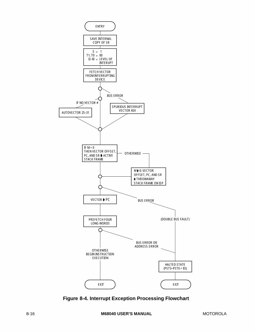
8-16 M68040 USER’S MANUAL MOTOROLA
EXIT
FETCH VECTOR FROM INTERRUPTING
DEVICE
PREFETCH FOUR LONG WORDS
VECTOR PC
OTHERWISE BEGIN INSTRUCTION
EXECUTION
BUS ERROR
BUS ERROR OR ADDRESS ERROR
HALTED STATE (PST3–PST0 = $5)
ENTRY
EXIT
SAVE INTERNAL COPY OF SR
S T1, T0
I2–I0
1 00 LEVEL OF INTERUPT
= = =
AUTOVECTOR 25–31
SPURIOUS INTERRUPT VECTOR #24
BUS ERROR
IF NO VECTOR #
OTHERWISE
IF M = 0 THEN VECTOR OFFSET, PC, AND SR ACTIVE STACK FRAME
M 0; VECTOR OFFSET, PC, AND SR THROWAWAY STACK FRAME ON ISP
(DOUBLE BUS FAULT)
Figure 8-4. Interrupt Exception Processing Flowchart

MOTOROLA M68040 USER’S MANUAL 8-17
8.2.10 Reset Exception
Asserting the reset in (RSTI) input signal causes a reset exception. The reset exceptionhas the highest priority of any exception; it provides for system initialization and recoveryfrom catastrophic failure. Reset also aborts any processing in progress when RSTI isrecognized; processing cannot be recovered. Figure 8-5 is a flowchart of the resetexception processing.
The reset exception places the processor in the interrupt mode of the supervisor privilegemode by setting the S-bit and clearing the M-bit and disables tracing by clearing the T1and T0 bits in the SR. This exception also sets the processor’s interrupt priority mask inthe SR to the highest level, level 7. Next the VBR is initialized to zero ($00000000), andthe enable bits in the cache control register (CACR) for the on-chip caches are cleared.The reset exception also clears the enable bit but does not affect page size in thetranslation control registers. It clears the enable bit in each of the four transparenttranslation registers. An interrupt acknowledge bus cycle is begun to generate a vectornumber. This vector number references the reset exception vector (two long words, vectornumbers 0 and 1) at offset zero in the supervisor address space. The first long word isloaded into the interrupt stack pointer, and the second long word is loaded into the PC.Reset exception processing concludes with the prefetch of the first four long wordsbeginning at the memory location pointed to by the PC.

8-18 M68040 USER’S MANUAL MOTOROLA
EXIT
FETCH VECTOR #0
FETCH VECTOR #1
PREFETCH 4 LONG WORDS
(DOUBLE BUS FAULT)
SPVECTOR #0
VECTOR #1
S M
T1, T0 I2:I0 VBR
CACR DTTn[E-bit] ITTn[E-bit]
1 0 0 $7 $0 $0 0 0=
= = = = = = =
EXIT
(DOUBLE BUS FAULT)
(DOUBLE BUS FAULT)
ENTRY
OTHERWISE BEGIN INSTRUCTION
EXECUTION
OTHERWISEBUS ERROR
BUS ERROR
BUS ERROR OR ADDRESS ERROR
HALTED STATE (PST3–PST0 = $5)
OTHERWISE
PC
Figure 8-5. Reset Exception Processing Flowchart
After the initial instruction is prefetched, program execution begins at the address in thePC. The reset exception does not flush the ATCs or invalidate entries in the instruction ordata caches; it does not save the value of either the PC or the SR. If an access fault oraddress error occurs during the exception processing sequence for a reset, a double busfault is generated. The processor halts, and the processor status (PST3–PST0) signalsindicate $5. Execution of the reset instruction does not cause a reset exception, or affect

MOTOROLA M68040 USER’S MANUAL 8-19
any internal registers, but it does cause the M68040 to assert the reset out (RSTO) signal,resetting all external devices.
8.3 EXCEPTION PRIORITIES
When several exceptions occur simultaneously, they are processed according to a fixedpriority. Table 8-4 lists the exceptions, grouped by characteristics. Each group has apriority, from 0–7, with 0 as the highest priority.
Table 8-4. Exception Priority Groups
Group/Priority
Exception and Relative Priority Characteristics
0 Reset Aborts all processing (instruction or exception) and does notsave old context.
1 Data Access Error(ATC Fault or Bus Error)
Aborts current instructions; can have pending trace, floating-point post-instruction, or unimplemented floating-pointinstruction exceptions.
2 Floating-Point Pre-Instruction* Exception processing begins before current floating-pointinstruction is executed. Instruction is restarted on return fromexception.
3 BKPT #n, CHK, CHK2, Divide by Zero,FTRAPcc, RTE, TRAP#n, TRAPV
Illegal Instruction, Unimplemented A- andF-Line, Privilege Violation
Unimplemented Floating-Point Instruction*
Exception processing is part of instruction execution.
Exception processing begins before instruction is executed.
Exception processing begins after memory operands arefetched and before instruction is executed.
4 Floating-Point Post-Instruction* Only reported for FMOVE to memory. Exception processingbegins when FMOVE instruction and previous exceptionprocessing have completed.
5 Address Error Reported after all previous instructions and associatedexceptions have completed.
6 Trace Exception processing begins when current instruction orprevious exception processing has completed.
7 Instruction Access Error(ATC Fault or Bus Error)
Reported after all previous instructions and associatedexceptions have completed.
8 Interrupt Exception processing begins when current instruction orprevious exception processing has completed.
* Refer to Section 9 Floating-Point Unit (MC68040 Only) for details concerning floating-point instructions.
The method used to process exceptions in the M68040 is significantly different from thatused in earlier members of the M68000 processor family due to the restart exceptionmodel. In general, when multiple exceptions are pending, the exception with the highestpriority is processed first, and the remaining exceptions are regenerated when the currentinstruction restarts. Note that the reset operation clears all other exceptions except in thefollowing circumstances:
• As soon as the M68040 has completed exception processing for a condition when aninterrupt exception is pending, it begins exception processing for the interrupt

8-20 M68040 USER’S MANUAL MOTOROLA
exception instead of executing the exception handler for the original exceptioncondition. For example, if simultaneous interrupt and trap exceptions are pending, theexception processing for the trap exception occurs first, followed immediately byexception processing for the interrupt. When the processor resumes normalinstruction execution, it is in the interrupt handler, which returns to the trap exceptionhandler.
• Exception processing for access error exceptions creates a format $7 stack framethat contains status information that can indicate a pending trace, floating-point post-instruction, or unimplemented floating-point instruction exception. The RTE instructionused to return from the access error exception handler checks the status bits for oneof these pending exceptions. If one is indicated, the RTE changes the access errorstack frame to match the pending exception and fetches the vector for the exception.Instruction execution then resumes in the new exception handler.
• If an access error, trace, and one of the two (mutually exclusive) floating-pointexceptions occur simultaneously, the pending floating-point exception is indicated inthe access error stack and the trace exception flag is undefined. The exceptionhandler for the floating-point exception must check the trace bits on the stack and callthe trace handler directly (after adjusting the stack frame to match the format for thetrace exception).
• If a trace exception is pending at the same time an exception priority level 3 orfloating-point post-instruction exception is pending, the trace exception is notreported, and the exception handler for the other exception condition must check forthe trace condition.
8.4 RETURN FROM EXCEPTIONS
After the processor has completed executing the exception handlers for all pendingexceptions, the processor resumes normal instruction execution at the address in theprocessor’s vector table for the last exception processed. Once the exception handler hascompleted execution, if possible the processor must return the system context as it wasprior to the exception using the RTE instruction. (If the internal data of the exception stackframes are manipulated, M68040 may enter into an undefined state; this appliesspecifically to the SSW on the access error stack frame.)
When the processor executes an RTE instruction, it examines the stack frame on top ofthe active supervisor stack to determine if it is a valid frame and what type of contextrestoration it requires. If during restoration, a stack frame has an odd address PC and anSR that indicates user trace mode enabled, then an address error is taken. The SRstacked for the address error has the SR S-bit set. For previous members of the M68000family the S-bit is clear. When the M68040 writes or reads a stack frame, it uses long-word operand transfers wherever possible. Using a long-word-aligned stack pointergreatly enhances exception processing performance. The processor does not necessarilyread or write the stack frame data in sequential order. The system software should notdepend on a particular exception generating a particular stack frame. For compatibilitywith future devices, the software should be able to handle any format of stack frame forany type of exception. The following paragraphs discuss in detail each stack frame format.
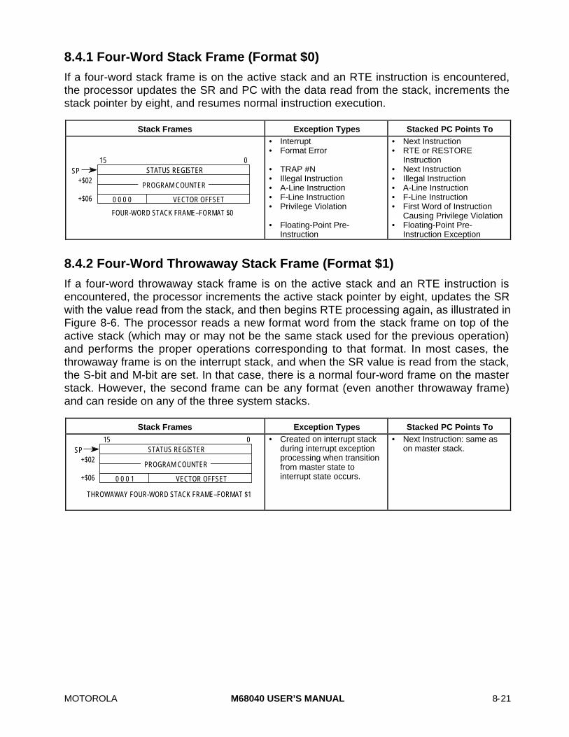
MOTOROLA M68040 USER’S MANUAL 8-21
8.4.1 Four-Word Stack Frame (Format $0)
If a four-word stack frame is on the active stack and an RTE instruction is encountered,the processor updates the SR and PC with the data read from the stack, increments thestack pointer by eight, and resumes normal instruction execution.
Stack Frames Exception Types Stacked PC Points To
STATUS REGISTER
PROGRAM COUNTER
0 0 0 0 VECTOR OFFSET
015SP
+$02
+$06
FOUR-WORD STACK FRAME–FORMAT $0
• Interrupt• Format Error
• TRAP #N• Illegal Instruction• A-Line Instruction• F-Line Instruction• Privilege Violation
• Floating-Point Pre-Instruction
• Next Instruction• RTE or RESTORE
Instruction• Next Instruction• Illegal Instruction• A-Line Instruction• F-Line Instruction• First Word of Instruction
Causing Privilege Violation• Floating-Point Pre-
Instruction Exception
8.4.2 Four-Word Throwaway Stack Frame (Format $1)
If a four-word throwaway stack frame is on the active stack and an RTE instruction isencountered, the processor increments the active stack pointer by eight, updates the SRwith the value read from the stack, and then begins RTE processing again, as illustrated inFigure 8-6. The processor reads a new format word from the stack frame on top of theactive stack (which may or may not be the same stack used for the previous operation)and performs the proper operations corresponding to that format. In most cases, thethrowaway frame is on the interrupt stack, and when the SR value is read from the stack,the S-bit and M-bit are set. In that case, there is a normal four-word frame on the masterstack. However, the second frame can be any format (even another throwaway frame)and can reside on any of the three system stacks.
Stack Frames Exception Types Stacked PC Points To
STATUS REGISTER
PROGRAM COUNTER
0 0 0 1 VECTOR OFFSET
015SP
+$02
+$06
THROWAWAY FOUR-WORD STACK FRAME–FORMAT $1
• Created on interrupt stackduring interrupt exceptionprocessing when transitionfrom master state tointerrupt state occurs.
• Next Instruction: same ason master stack.

8-22 M68040 USER’S MANUAL MOTOROLA
EXIT
OTHER FORMATS
FORMAT CODE = $1(THROWAWAY
FRAME)
SR TEMP SP SP + 6
PC (SP) + SP SP + 6 SR TEMP
TEMP (SP)+READ FORMAT WORD
ENTRY
INVALID FORMAT WORD
OTHERWISE
OTHERWISE
FORMAT CODE = $0 (4-WORD FRAME)OTHERWISE
TAKE FORMAT ERROR EXCEPTION
Figure 8-6. Flowchart of RTE Instruction for Throwaway Four-Word Frame
8.4.3 Six-Word Stack Frame (Format $2)
If a six-word throwaway stack frame is on the active stack and an RTE instruction isencountered, the processor restores the SR and PC values from the stack, increments theactive supervisor stack pointer by $C, and resumes normal instruction execution.
Stack Frames Exception Types Stacked PC Points To
STATUS REGISTER
PROGRAM COUNTER
0 0 1 0 VECTOR OFFSET
015SP
+$02
+$06
SIX-WORD STACK FRAME–FORMAT $2
ADDRESS+$08
• CHK, CHK2, TRAPcc,FTRAPcc, TRAPV, Trace,or Zero Divide
• Unimplemented Floating-Point Instruction
• Address Error
• Next Instruction: address isthe address of theinstruction that caused theexception.
• Next Instruction: address isthe calculated <ea> for thefloating-point instruction.
• Instruction that caused theaddress error, address isthe reference address – 1.

MOTOROLA M68040 USER’S MANUAL 8-23
8.4.4 Floating-Point Post-Instruction Stack Frame (Format $3)
The processor restores the SR and PC values from the stack and increments the activesupervisor stack pointer by $C. If another floating-point post-instruction exception ispending, exception processing begins immediately for the new exception; otherwise, theprocessor resumes normal instruction execution.
Stack Frames Exception Types Stacked PC Points To
STATUS REGISTER
PROGRAM COUNTER
0 0 1 1 VECTOR OFFSET
015SP
+$02
+$06
FLOATING-POINT POST-INSTRUCTION STACK FRAME–FORMAT $3
EFFECTIVE ADDRESS+$08
• Floating-Point Post-Instruction
• Next Instruction: <ea> is thecalculated effective addressfor the floating-pointinstruction.
8.4.5 Eight-Word Stack Frame (Format $4)
The MC68040V, MC68LC040, MC68EC040, and MC68EC040V use this stack frame forunimplemented floating-point instructions. The MC68040 does not generate or recognizethis format stack frame. Refer to Appendix A MC68LC040 and Appendix B MC68EC040for further details about this stack frame.

8-24 M68040 USER’S MANUAL MOTOROLA
8.4.6 Access Error Stack Frame (Format $7)
A 30-word access error stack frame is created for data and instruction access faults otherthan instruction address errors. In addition to information about the current processorstatus and the faulted access, the stack frame also contains pending write-backs that theaccess error exception handler must complete. The following paragraphs describe indetail the format for this frame and how the processor uses it when returning fromexception processing.
Stack Frames Exception Types Stacked PC Points To
SPECIAL STATUS WORD (SSW)
$00 WRITE-BACK 1 STATUS (WB1S)
015SP
+$02
+$12
ACCESS ERROR STACK FRAME (30 WORDS)–FORMAT $7
FAULT ADDRESS (FA)+$14
WRITE-BACK 3 ADDRESS (WB3A)
WRITE-BACK 3 DATA (WB3D)
WRITE-BACK 1 DATA/PUSH DATA LW0 (WB1D/PD0)
PUSH DATA LW 1 (PD1)
WRITE-BACK 2 ADDRESS (WB2A)
WRITE-BACK 2 DATA (WB2D)
WRITE-BACK 1 ADDRESS (WB1A)
PUSH DATA LW 2 (PD2)
PUSH DATA LW 3 (PD3)
+$18
+$1C
+$20
+$24
+$28
+$2C
+$30
+$34
+$38
STATUS REGISTER
PROGRAM COUNTER
0 1 1 1 VECTOR OFFSET
EFFECTIVE ADDRESS (EA)
$00 WRITE-BACK 2 STATUS (WB2S)$00 WRITE-BACK 3 STATUS (WB3S)
+$10
+$0C+$0E
+$08+$0A
+$06
• Data or Instruction AccessFault (ATC Fault or BusError)
• Next Instruction
8.4.6.1 EFFECTIVE ADDRESS. The effective address contains address information whenone of the continuation flags CM, CT, CU, or CP in the SSW is set.
8.4.6.2 SPECIAL STATUS WORD (SSW). The SSW information indicates whether anaccess to the instruction stream or the data stream (or both) caused the fault and containsstatus information for the faulted access. Figure 8-7 illustrates the SSW format.
15 14 13 12 11 10 9 8 7 6 5 4 3 2 1 0
CP CU CT CM MA ATC LK RW X SIZE TT TM
Figure 8-7. Special Status Word Format

MOTOROLA M68040 USER’S MANUAL 8-25
CP—Continuation of Floating-Point Post-Instruction Exception PendingCP is set for an access error with a floating-point post-instruction exception pending. Allpending accesses are allowed to complete after a trace condition is recognized. If anyof these accesses fault, the resulting stack frame has the CT bit set, and the effectiveaddress field contains the address of the instruction being traced. The RTE fetches theappropriate floating-point post-instruction exception vector.
When a post-instruction exception occurs during tracing, the post-instruction exceptiontakes precedence. CP is set, and CT = 0 and can be traced. The kernel must check fora trace condition using the stacked SR. The effective address field contains thecalculated effective address determined by the effective address field of the floating-point instruction that caused the post-instruction exception.
CU—Continuation of Unimplemented Floating-Point Instruction Exception PendingCU is set for an access error with a pending exception for an unimplemented floating-point instruction. Operation is the same as for the CP flag except the RTE fetches theF-line exception vector. The effective address field contains the calculated effectiveaddress determined by the effective address field of the unimplemented instruction.
When an unimplemented floating-point instruction is traced, the unimplementedexception takes precedence, CU is set, and CT = 0. The kernel must check for a tracecondition using the stacked SR. If this condition is true, create the required stack frameand jump directly to the trace handler.
CT—Continuation of Trace Exception PendingCT is set for an access error with a pending trace exception. Operation is the same asfor the CP flag. When RTE is executed with CT set, the M68040 will move the words onthe stack an offset of $00–$0B from the current SP to offset $30–$3B, adjusting thestack pointer by +$30. The M68040 changes the stack frame format to $2 beforefetching the trace exception vector and jumping directly to trace exception handling.This stack adjustment creates the stack frame that normally would have been createdfor the trace exception had the pending access not encountered a bus error.
CM—Continuation of MOVEM Instruction Execution PendingCM is set if a data access encounters a bus error for a MOVEM. Since the MOVEMoperation can write over the memory location or registers used to calculate the effectiveaddress, the M68040 internally saves the effective address after calculation. WhenMOVEM encounters a bus error, a stack frame is created with CM set, and the effectiveaddress field contains the calculated effective address for the instruction. When RTE isexecuted, MOVEM restarts using the effective address on the stack (instead ofrepeating the effective address calculate operation) if the address mode is PC relative(mode = 111, register = 010 or 011) or indirect with index (mode = 110).
MA—Misaligned AccessMA is set if an ATC fault occurs for second-page access that spans two pages inmemory.
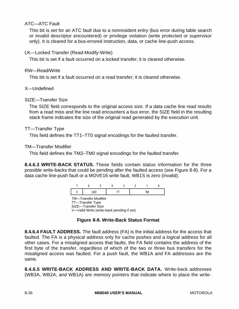
8-26 M68040 USER’S MANUAL MOTOROLA
ATC—ATC FaultThis bit is set for an ATC fault due to a nonresident entry (bus error during table searchor invalid descriptor encountered) or privilege violation (write protected or supervisoronly). It is cleared for a bus-errored instruction, data, or cache line-push access.
LK—Locked Transfer (Read-Modify-Write)This bit is set if a fault occurred on a locked transfer; it is cleared otherwise.
RW—Read/WriteThis bit is set if a fault occurred on a read transfer; it is cleared otherwise.
X—Undefined
SIZE—Transfer SizeThe SIZE field corresponds to the original access size. If a data cache line read resultsfrom a read miss and the line read encounters a bus error, the SIZE field in the resultingstack frame indicates the size of the original read generated by the execution unit.
TT—Transfer TypeThis field defines the TT1–TT0 signal encodings for the faulted transfer.
TM—Transfer ModifierThis field defines the TM2–TM0 signal encodings for the faulted transfer.
8.4.6.3 WRITE-BACK STATUS. These fields contain status information for the threepossible write-backs that could be pending after the faulted access (see Figure 8-8). For adata cache line-push fault or a MOVE16 write fault, WB1S is zero (invalid).
7 6 5 4 3 2 1 0
V SIZE TT TM
TM—Transfer ModifierTT—Transfer TypeSIZE—Transfer SizeV—Valid Write (write-back pending if set)
Figure 8-8. Write-Back Status Format
8.4.6.4 FAULT ADDRESS. The fault address (FA) is the initial address for the access thatfaulted. The FA is a physical address only for cache pushes and a logical address for allother cases. For a misaligned access that faults, the FA field contains the address of thefirst byte of the transfer, regardless of which of the two or three bus transfers for themisaligned access was faulted. For a push fault, the WB1A and FA addresses are thesame.
8.4.6.5 WRITE-BACK ADDRESS AND WRITE-BACK DATA. Write-back addresses(WB3A, WB2A, and WB1A) are memory pointers that indicate where to place the write-

MOTOROLA M68040 USER’S MANUAL 8-27
back data (WB3D, WB2D, and WB1D). WB3A and WB3D correspond to the temporaryholding register in the integer unit (WB3). WB2A and WB2D correspond to the temporaryholding register in the data memory unit (WB2) prior to address translation. WB1A andWB1D correspond to the temporary holding register in the bus controller (WB1), whichdetermines the external address and data bus bit patterns. Refer to Section 2 IntegerUnit for details on the operation of the integer unit pipeline.
The write-back data in WB3D and WB2D is register aligned with byte and word datacontained in the least significant byte and word, respectively, of the field. Write-back datain WB1D is memory aligned and resides in the byte positions corresponding to the databus lanes used in writing each byte to memory. Table 8-5 lists the data alignment for eachcombination of data format and A1 and A0.
Table 8-5. Write-Back Data Alignment
Address Data Alignment
Data Format A1 A0 WB1D WB2D, WB3D
Byte 0011
0101
31–2423–1615–87–0
7–07–07–07–0
Word 0011
0101
31–1623–815–0
7–0, 31–24
15–015–015–015–0
Long Word 0011
0101
31–023–0, 31–2415–0, 31–167–0, 31–8
31–031–031–031–0
NOTE: For a line transfer fault, the four long words of data in PD3–PD0 are already aligned with memory. Bits 31–0 of each fieldcorrespond to bits 31–0 of the memory location to be written to,regardless of the value of the address bits A1 and A0 for thewrite-back address.
8.4.6.6 PUSH DATA. The push data field contains an image of the cache line that needsto be pushed to memory.
8.4.6.7 ACCESS ERROR STACK FRAME RETURN FROM EXCEPTION. For the accesserror stack frame (format $7), the processor restores the SR and PC values from the stackand checks the four continuation status bits in the SSW on the stack. If these bits are notset, the processor increments the active supervisor stack pointer by 30 words andresumes normal instruction execution. If the MOVEM continuation bit is set, the processorrestores the calculated effective address from the stack frame, increments the activesupervisor stack pointer by 30 words, and restarts the MOVEM instruction at a point afterthe effective address calculation. All operand accesses for the MOVEM that occurredbefore the faulted access are repeated. If a continuation bit is set for a pending trace,unimplemented floating-point instruction, or floating-point post-instruction exception, theprocessor restores the calculated effective address from the stack frame, increments theactive supervisor stack pointer by 30 words, and immediately begins exception processing

8-28 M68040 USER’S MANUAL MOTOROLA
for the pending exception. The processor sets only one of the continuation bits when theaccess error stack frame is created. If the access error exception handler sets multiplebits, operation of the RTE instruction is undefined.
If the frame format field in the stack frame contains an illegal format code, a formatexception occurs. If a format error or access fault exception occurs during the framevalidation sequence of the RTE instruction, the processor creates a normal four-word oran access error stack frame below the frame that it was attempting to use. The illegalstack frame remains intact, so that the exception handler can examine or repair the illegalframe. In a multiprocessor system, the illegal frame can be left so that, when appropriate,another processor of a different type can use it.
The bus error exception handler can identify bus error exceptions due to instruction faultsby examining the TM field in the SSW of the access error stack frame. For user andsupervisor instruction faults, the TM field contains $2 and $6, respectively (see Figure8-7). Since the processor allows all pending accesses to complete before reporting aninstruction fault, the stack frame for an instruction fault will not contain any pending write-backs. The ATC bit of the SSW is used to distinguish between ATC faults and physicalbus errors, and the FA field contains the logical address of the instruction prefetch. ForATC faults, the exception handler can execute a PTEST instruction (using the FA and TMfields from the SSW) to determine the specific cause of the address translation failure.After the handler corrects the cause of the fault, it executes an RTE instruction to restartexecution of the instruction that contained the faulted prefetch.
For an address error fault, the processor saves a format $2 exception stack frame on thestack. This stack frame contains the PC pointing to the instruction that caused the addresserror as well as the actual address referenced by the instruction. Note that bit 0 of thereferenced address is cleared on the stack frame. Address error faults must be repaired insoftware.
For a fault due to a data ATC fault or bus error, pending write-backs are also saved on theaccess error stack frame and must be completed by the exception handler. For the faultedaccess, the fault address in the FA field combined with the transfer attribute informationfrom the SSW can be used to identify the cause of the fault. In identifying the fault, thesystem programmer should be aware that the data memory unit considers the read portionof read-modify-write transfers (for TAS, CAS, CAS2, and some translation table updates)a write. This prevents both read and write accesses from occurring unless all pagestouched by the instruction or table update are write enabled.
All accesses other than instruction prefetches go through the data memory unit, and theM68040 treats the instruction and data address spaces as a single merged address space(the exception is the presence of separate transparent translation registers). The functioncodes for accesses such as PC relative operand addressing and MOVES transfers tofunction codes $2 and $6 (user and supervisor instruction spaces in the MC68000) areconverted to data references to go through the data memory unit, and appear in the TMfield of the access error stack frame as data references.

MOTOROLA M68040 USER’S MANUAL 8-29
After the fault is corrected, any pending write-backs on the stack frame must becompleted. The write-back status fields should be checked for possible write-backs, whichthe exception handler should complete in the following order: write-back 1, write-back 2,and write-back 3. For a push fault, the push must be completed first, followed by twopotential write-backs. Completion of write-back 1 should not generate another accesserror since this write-back corresponds to the faulted access that has been corrected bythe handler. However, write-backs 2 and 3 can cause another bus error exception whenthe handler attempts to write to memory and should be checked before attempting thewrite to prevent nesting of exceptions if required by the operating system. The followinggeneral bus fault examples indicate the resulting contents of the access error stack framefields:
1. All Read Access Errors (SSW–RW = $1, TT = $0, TM = $1 or $5)—The FA fieldcontains the logical address of the fault. The WB1S and WB2S fields are zero, andonly WB3S can indicate an additional write-back.
2. Cache Push Physical Bus Error (SSW–RW = $0, TT = $0, TM = $0)—The assertionof TEA causes this error when a cache push bus cycle is in progress. The FA fieldcontains the physical address of the fault, and the WB1S field is ignored. All fourlong words of the data for a push are contained in LW3–LW0 regardless of the sizeof the transfer. The size of the transfer is indicated in the SIZE field of the SSW andcan be either a line or long word. If a line is indicated, all four long words need to bepushed out. If a long word is indicated, all four long words can be written out, or bits3 and 2 of the FA field can be evaluated to indicate which long words need to bewritten out to memory ($3, $2, $1, and $0 indicate LW3, LW2, LW1, and LW0,respectively). The WB2S and WB3S fields indicate up to two additional write-backs.If WB2S is valid and if it indicates a MOVE16 instruction, no data should be writtenout for that write-back slot.
3. Normal Write Physical Bus Error (SSW–RW = $0, TT = $0, TM = $1 or $5)—Theassertion of TEA causes this error when a normal write bus cycle is in progress. TheFA field contains the logical address of the fault, and the WB1S field indicates that itis valid. The FA and WB1A are equivalent. The WB2S and WB3S fields indicate upto two additional write-backs.
4. MOVE16 Write Physical Bus Error (SSW–RW = $0, TT = $1)—The assertion of TEAcauses this error during the write portion of a MOVE16 instruction. The FA fieldcontains the logical address of the fault, and the WB1S field indicates that it is valid.All four long words are contained in LW3–LW0 and must be written out before usingFA. Software must ensure that address bits 1 and 0 are both clear if regular moveinstruction are to be used to write out to the destination.
5. Page Fault (SSW–RW = $0, WB1S–V = $0)—The FA field contains the physicaladdress of the faulted instruction, WB1S = 0, and WB2S indicates that it is valid.Only WB3S can indicate an additional write-back. If WB2S indicates a MOVE16instruction and if the MOVE16 instruction is used to read from a peripheral thatcannot tolerate double reads, then software must write the data contained in PD3–PD0 out to memory and increment the stacked PC to take it beyond the MOVE16instruction that caused the page fault. Otherwise, if the MOVE16 instruction isallowed to be restarted, another read from the peripheral would occur. If doublereads can be tolerated, simply do no write-backs and allow instruction to restart. Thisis the only case in which the action to be taken depends on whether or not a doubleread can be tolerated.

8-30 M68040 USER’S MANUAL MOTOROLA
Table 8-6 lists the possible combinations of write-backs and the proper way to handlethem. The SSW_RW column indicates a read or write cycle; the SSW_PUSH columnindicates whether the fault is for a push (TT = 00 and TM = 000). The WB1S, WB2S, andWB3S columns list the respective field’s V-bit and indicate a MOVE16 transfer type (TT =01). The easy cleanup data written column lists the stack’s field to be written out tomemory if the user is not concerned with retouching peripherals. The hard cleanup actioncolumn lists the action to be taken if the peripherals cannot be retouched by MOVE16 (ifdifferent from easy cleanup). Note that if a push access error is reported and the size islong word, all four long words, PD0–PD3, are still valid for the line. The exception handlercan either write PD0–PD3 using the fault address with bits 3–0 cleared or write the PDcorresponding to bits 3–2 of the address (e.g., address $0000000C corresponds to PD3).Note that a MOVE16 is never reported in the WB3S. The SIZE field of WB3S is never aline.
After the bus error exception handler completes all pending operations and executes anRTE to return, the RTE reads only the stack information from offset $0–$D in the accesserror stack frame. For a pending trace exception, unimplemented floating-point instructionexception, or floating-point post-instruction exception, the RTE adjusts the stack to matchthe pending exception and immediately begins exception processing, without requiring theexception to reoccur.

MOTOROLA M68040 USER’S MANUAL 8-31
Table 8-6. Access Error Stack Frame Combinations
WB1S WB2S WB3S Easy Cleanup Hard CleanupMain Case SSW_RW SSW_PUSH 1V 1M16 2V 2M16 3V Data Written Action
All ReadAccess Errors
1a
1aNoNo
00
XX
00
XX
01
NoneWB3D (Note b)
All other read cases are not possible.
Cache PushPhysical BusErrorc
00000
YesYesYesYesYes
00000
XXXXX
00111
XX001
01010
PD3–0PD3–0, WB3DPD3–0, WB2DPD3–0, WB2D, WB3DPD3–0, ~WB2Dd
(Note b)
Normal WritePhysical busError
00000
NoNoNoNoNo
11111
00000
00111
XX001
01010
WB1DWB1D, WB3DWB1D, WB2DWB1D, WB2D, WB3DWB1D, ~WB2Dd
(Note b)
MOVE16Write PhysicalBus Error
00000
NoNoNoNoNo
11111
11111
00111
XX001
10010
PD3–0, WB3DPD3–0PD3–0, WB2DPD3–0, WB2D, WB3DPD3–0, ~WB2Dd
(Note b)
Write PageFault
000
NoNoNo
000
XXX
111
001
010
WB2DWB2D, WB3D~WB2Dd
Write PD3–0and skipe.
ImpossibleWrite Cases
00
YesDon't Care
1X
XX
XX
X1
X1
(Note f)(Note g)
—
NOTES:a. The data memory unit stage is tied up until the bus controller passes the read back through the data memory
unit and to the execution stage in the integer unit. Therefore, no pending write is possible in WB1 or WB2.WB3 could hold a pending write that was deferred due to operand read or was generated after the read.
b. If any kind of access error is reported and if a MOVE16 write is pending in the WB2 stage, then that MOVE16read must hit in the cache so the MOVE16 can be safely restarted since it has not caused bus cycles that couldretouch peripherals.
c. A cache push physical bus error is normally considered a fatal error. For these cases, the FA field is a physicaladdress, not a logical address as in the other cases.
d. Indicates that the data should not be written even though the V-bit for it is set (WB2 corresponds to a MOVE16write).
e. The exception handler must alter the stacked PC to point past the MOVE16 and predecrement andpostincrement address registers.
f. 1V must be 0 for push exceptions.g. The execution stage does not post a write until the MOVE16 is in the integer unit.

8-32 M68040 USER’S MANUAL MOTOROLA
MOTOROLA M68040 USER’S MANUAL 9-1
SECTION 9FLOATING-POINT UNIT (MC68040 ONLY)
NOTE
This section does not apply to the MC68040V, MC68LC040,MC68EC040, or MC68EC040V. Refer to Appendix AMC68LC040 and Appendix B MC68EC040 for details.
Floating-point math refers to numeric calculations with a variable decimal point location. Itis distinguished from integer math, which deals only with whole numbers and fixeddecimal point locations. Historically, general-purpose microprocessors have had todepend on add-on coprocessors and accelerators such as the MC68881/MC68882 for fastfloating-point capabilities. The MC68040 features a built-in floating-point unit (FPU).Consolidating this important function on chip speeds up the overall processing andeliminates some interfacing overhead required for external accelerators. The MC68040FPU operates in parallel with the integer unit (IU). The FPU does the numeric calculationwhile the IU moves on to other tasks. Like the IU, the FPU has its own three-stagepipeline overlapping operations such as integer to floating-point conversion, instructionexecution, and write-back. When used with the M68040FPSP, the MC68040 FPU is fullycompliant with IEEE floating-point standards.
9.1 FLOATING-POINT UNIT PIPELINE
Integer data from memory (memory to register) requires a pass through the FPU pipeline,converting the data to the extended-precision format for the FPU to use. The result of thisconversion is presented to the conversion stage of the FPU pipeline where the desiredoperation begins, starting a second pass through the pipeline. The IU is then released toexecute other instructions once the data has been transferred to the FPU.
Floating-point data to memory (register to memory) requires a complete pass through theFPU pipeline, converting the data from the extended-precision format to an integer dataformat. Register-to-memory instructions are normally handled entirely by the conversionstage of the pipeline where the data move to memory operation completes. The IU is notreleased until it has received the converted data (during the last conversion unit cycle).
Like the IU, the FPU has been optimized for the most frequently used instructions anddata types to provide the highest possible performance. To boost performance further, theFMOVE instruction concurrently executes with arithmetic calculations and executescompletely transparent to the user. Instructions can execute nonsequentially as long asthere are no register dependencies. Refer to Section 10 Instruction Timings for detailson floating-point timings.
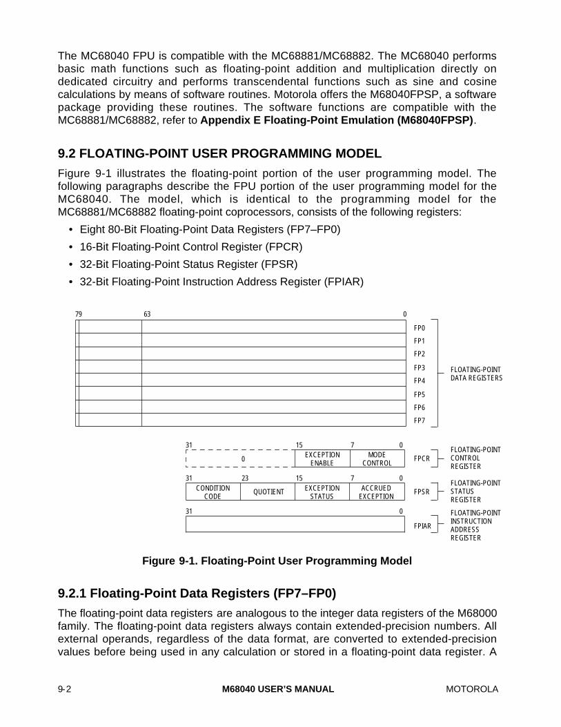
9-2 M68040 USER’S MANUAL MOTOROLA
The MC68040 FPU is compatible with the MC68881/MC68882. The MC68040 performsbasic math functions such as floating-point addition and multiplication directly ondedicated circuitry and performs transcendental functions such as sine and cosinecalculations by means of software routines. Motorola offers the M68040FPSP, a softwarepackage providing these routines. The software functions are compatible with theMC68881/MC68882, refer to Appendix E Floating-Point Emulation (M68040FPSP).
9.2 FLOATING-POINT USER PROGRAMMING MODEL
Figure 9-1 illustrates the floating-point portion of the user programming model. Thefollowing paragraphs describe the FPU portion of the user programming model for theMC68040. The model, which is identical to the programming model for theMC68881/MC68882 floating-point coprocessors, consists of the following registers:
• Eight 80-Bit Floating-Point Data Registers (FP7–FP0)
• 16-Bit Floating-Point Control Register (FPCR)
• 32-Bit Floating-Point Status Register (FPSR)
• 32-Bit Floating-Point Instruction Address Register (FPIAR)
79 63 0
FP0
FP1
FP3
FP4
FP5
FP6
FP7
FP2
FLOATING-POINT DATA REGISTERS
FPCRFLOATING-POINT CONTROL REGISTER
FPSRFLOATING-POINT STATUS REGISTER
FPIAR
FLOATING-POINT INSTRUCTION ADDRESS REGISTER
071531MODE
CONTROLEXCEPTION
ENABLE0
EXCEPTION STATUS
CONDITION CODE
QUOTIENT ACCRUED EXCEPTION
071531 23
031
Figure 9-1. Floating-Point User Programming Model
9.2.1 Floating-Point Data Registers (FP7–FP0)
The floating-point data registers are analogous to the integer data registers of the M68000family. The floating-point data registers always contain extended-precision numbers. Allexternal operands, regardless of the data format, are converted to extended-precisionvalues before being used in any calculation or stored in a floating-point data register. A
MOTOROLA M68040 USER’S MANUAL 9-3
reset or a restore operation of the null state sets FP7–FP0 to positive, nonsignaling not-a-numbers (NANs).
9.2.2 Floating-Point Control Register (FPCR)
The FPCR (see Figure 9-2) contains an exception enable (ENABLE) byte that enables ordisables traps for each class of floating-point exceptions and a mode control (MODE) bytethat sets the user-selectable modes. The user can read or write to the FPCR. Motorolareserves bits 31–16 for future definition; these bits are always read as zero and areignored during write operations. The reset function or a restore operation of the null stateclears the FPCR. When cleared, this register provides the IEEE 754 standard defaults.
9.2.2.1 EXCEPTION ENABLE BYTE. Each bit of the ENABLE byte (see Figure 9-2)corresponds to a floating-point exception class. The user can separately enable traps foreach class of floating-point exceptions.
9.2.2.2 MODE CONTROL BYTE. The MODE byte (see Figure 9-2) controls the user-selectable rounding modes and precisions. Zeros in this byte select the IEEE 754standard defaults. The rounding mode (RND) specifies how inexact results are rounded,and the rounding precision (PREC) selects the boundary for rounding the mantissa.
The processor supports four rounding modes specified by the IEEE 754 standard. Thesemodes are: round to nearest (RN), round toward zero (RZ), round toward plus infinity(RP), and round toward minus infinity (RM). The RP and RM modes are directed roundingmodes that are useful in interval arithmetic. Rounding is accomplished through theintermediate result. Single-precision results are rounded to a 24-bit boundary; double-precision results are rounded to a 53-bit boundary; and extended-precision results arerounded to a 64-bit boundary. Table 9-1 lists the encodings for the FPCR.
Table 9-1. Floating-Point Control Register Encodings
Rounding Mode(RND Field)
Encoding Rounding Precision(PREC Field)
To Nearest (RN) 0 0 Extend (X)
Toward Zero (RZ) 0 1 Single (S)
Toward Minus Infinity (RM) 1 0 Double (D)
Toward Plus Infinity (RP) 1 1 Undefined

9-4 M68040 USER’S MANUAL MOTOROLA
15 14
EXCEPTION ENABLE
12 11 10 9 8
INEXACT DECIMAL INPUTINEXACT OPERATIONDIVIDE BY ZEROUNDERFLOWOVERFLOWOPERAND ERRORSIGNALING NOT-A-NUMBER BRANCH/SET ON UNORDERED
7 6 5 4 3 2 1 0
SNAN OPERR OVFL UNFL DZ INEX2 INEX1BSUN PREC RND 0
ROUNDING PRECISIONROUNDING MODE
MODE CONTROL
13
Figure 9-2. Floating-Point Control Register
9.2.3 Floating-Point Status Register (FPSR)
The FPSR (see Figure 9-1) contains a floating-point condition code (FPCC) byte, aquotient byte, a floating-point exception status byte (EXC), and a floating-point accruedexception byte (AEXC). The user can read or write to all bits in the FPSR. Execution ofmost floating-point instructions modifies this register. The reset function or a restoreoperation of the null state clears the FPSR. Floating-point conditional operations are notguaranteed if the FPSR is written directly, because the FPSR is only valid as a result of afloating-point instruction.
9.2.3.1 FLOATING-POINT CONDITION CODE BYTE. The FPCC byte (see Figure 9-3)contains four condition code bits that are set at the end of all arithmetic instructionsinvolving the floating-point data registers. These bits are sign of mantissa (N), zero (Z),infinity (I), and NAN. The FMOVE FPm,< ea>, FMOVEM FPm, and FMOVE FPCRinstructions do not affect the FPCC.
N Z I NAN
31 30 29 28 27 26 25 24
NOT-A-NUMBER OR UNORDERED
INFINITY
ZERO
NEGATIVE
0
Figure 9-3. FPSR Condition Code Byte
To aid programmers of floating-point subroutine libraries, the MC68040 implements thefour FPCC bits in hardware instead of only implementing the four IEEE conditions. Aninstruction derives the IEEE conditions when needed. For example, the programmers of acomplex arithmetic multiply subroutine usually prefer to handle special data types such as

MOTOROLA M68040 USER’S MANUAL 9-5
zeros, infinities, or NANs separately from normal data types. The floating-point conditioncodes allow users to efficiently detect and handle these special values.
9.2.3.2 QUOTIENT BYTE. The quotient byte (see Figure 9-4) provides compatibility withthe MC68881/MC68882 FPU. This byte contains the seven least significant bits of theunsigned quotient as well as the sign of the entire quotient.
The quotient bits can be used in argument reduction for transcendentals and otherfunctions. For example, seven bits are more than enough to determine the quadrant of acircle in which an operand resides. The quotient field (bits 22–16) remains set until theuser clears it.
23 22 21 20 19 18 17 16
SEVEN LEAST SIGNIFICANT BITS OF QUOTIENT
S QUOTIENT
SIGN OF QUOTIENT
Figure 9-4. FPSR Quotient Byte
9.2.3.3 EXCEPTION STATUS BYTE. The EXC byte (see Figure 9-5) contains a bit foreach floating-point exception that can occur during the most recent arithmetic instructionor move operation. The start of most operations clears this byte; however, operations thatcannot generate floating-point exceptions do not clear this byte. An exception handler canuse this byte to determine which floating-point exception(s) caused a trap.
BRANCH/SET ON UNORDERED
SNAN OPERR OVFL UNFL DZ INEX2 INEX1
15 14 13 12 11 10 9 8
INEXACT DECIMAL INPUT
INEXACT OPERATION
DIVIDE BY ZERO
UNDERFLOWOVERFLOW
OPERAND ERROR
SIGNALING NOT-A-NUMBER
BSUN
Figure 9-5. FPSR Exception Status Byte
9.2.3.4 ACCRUED EXCEPTION (AEXC) BYTE. The AEXC byte contains five exceptionbits (see Figure 9-6) that the IEEE 754 standard requires for exception disabledoperations. These exceptions are logical combinations of the bits in the EXC byte. TheAEXC byte contains the history of all floating-point exceptions that have occurred sincethe user last cleared the AEXC byte. In normal operations, only the user clears this byteby writing to the FPSR; however, a reset or a restore operation of the null state can alsoclear the AEXC byte.
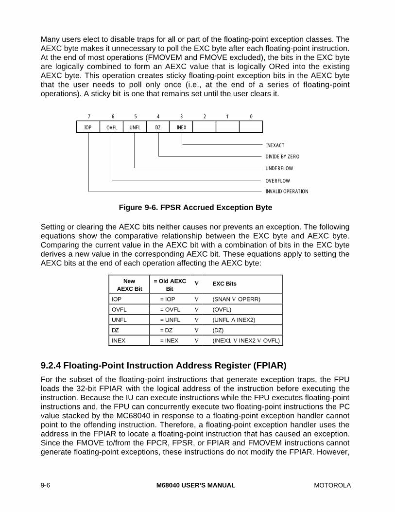
9-6 M68040 USER’S MANUAL MOTOROLA
Many users elect to disable traps for all or part of the floating-point exception classes. TheAEXC byte makes it unnecessary to poll the EXC byte after each floating-point instruction.At the end of most operations (FMOVEM and FMOVE excluded), the bits in the EXC byteare logically combined to form an AEXC value that is logically ORed into the existingAEXC byte. This operation creates sticky floating-point exception bits in the AEXC bytethat the user needs to poll only once (i.e., at the end of a series of floating-pointoperations). A sticky bit is one that remains set until the user clears it.
IOP OVFL UNFL DZ INEX
7 6 5 4 3 2 1 0
INEXACT
INVALID OPERATION
DIVIDE BY ZERO
UNDERFLOW
OVERFLOW
Figure 9-6. FPSR Accrued Exception Byte
Setting or clearing the AEXC bits neither causes nor prevents an exception. The followingequations show the comparative relationship between the EXC byte and AEXC byte.Comparing the current value in the AEXC bit with a combination of bits in the EXC bytederives a new value in the corresponding AEXC bit. These equations apply to setting theAEXC bits at the end of each operation affecting the AEXC byte:
NewAEXC Bit
= Old AEXCBit
V EXC Bits
IOP = IOP V (SNAN V OPERR)
OVFL = OVFL V (OVFL)
UNFL = UNFL V (UNFL Λ INEX2)
DZ = DZ V (DZ)
INEX = INEX V (INEX1 V INEX2 V OVFL)
9.2.4 Floating-Point Instruction Address Register (FPIAR)
For the subset of the floating-point instructions that generate exception traps, the FPUloads the 32-bit FPIAR with the logical address of the instruction before executing theinstruction. Because the IU can execute instructions while the FPU executes floating-pointinstructions and, the FPU can concurrently execute two floating-point instructions the PCvalue stacked by the MC68040 in response to a floating-point exception handler cannotpoint to the offending instruction. Therefore, a floating-point exception handler uses theaddress in the FPIAR to locate a floating-point instruction that has caused an exception.Since the FMOVE to/from the FPCR, FPSR, or FPIAR and FMOVEM instructions cannotgenerate floating-point exceptions, these instructions do not modify the FPIAR. However,

MOTOROLA M68040 USER’S MANUAL 9-7
they can be used to read the FPIAR in an exception handler without changing theprevious value. A reset or a restore operation of the null state clears the FPIAR.
9.3 FLOATING-POINT DATA FORMATS AND DATA TYPES
The M68000 floating-point model (MC68881, MC68882, MC68040) supports the followingdata formats: single precision, double precision, extended precision, and packed decimal.The M68000 floating-point model supports the following data types: normalized, zeros,infinities, denormalized numbers, and NANs. The MC68040 supports part of the M68000floating-point model in hardware. Table 9-2 lists the data formats and data typessupported by the MC68040. Tables 9-3 through 9-6 summarize the floating-point dataformats and data types details. For further information on the data formats and data types,refer to the M68000UM/AD, M68000 Family Programmer’s Reference Manual.
Table 9-2. MC68040 FPU Data Formats and Data Types
Data Formats
NumberTypes
Single-Precision
Real
Double-Precision
Real
Extended-Precision
Real
Packed-Decimal
RealByte
IntegerWord
Integer
Long-Word
Integer
Normalized * * * † * * *
Zero * * * † * * *
Infinity * * * †
NAN * * * †
Denormalized † † † †
Unnormalized † †
*Data Format/Type Supported by On-Chip MC68040 FPU Hardware†Data Format/Type Supported by Software (MC68040FPSP)

9-8 M68040 USER’S MANUAL MOTOROLA
Table 9-3. Single-Precision Real Format Summary
Data Format
s e f31 30 23 22 0
Field Size In Bits
Sign (s) 1
Biased Exponent (e) 8
Fraction (f) 23
Total 32
Interpretation of Sign
Positive Fraction s = 0
Negative Fraction s = 1
Normalized Numbers
Bias of Biased Exponent +127 ($7F)
Range of Biased Exponent 0 < e < 255 ($FF)
Range of Fraction Zero or Nonzero
Fraction 1.f
Relation to Representation of Real Numbers (–1)s × 2e–127 × 1.f
Denormalized Numbers
Biased Exponent Format Minimum 0 ($00)
Bias of Biased Exponent +126 ($7E)
Range of Fraction Nonzero
Fraction 0.f
Relation to Representation of Real Numbers (–1)s × 2–126 × 0.f
Signed Zeros
Biased Exponent Format Minimum 0 ($00)
Fraction 0.f = 0.0
Signed Infinities
Biased Exponent Format Maximum 255 ($FF)
Fraction 0.f = 0.0
NANs
Sign Don’t Care
Biased Exponent Format Maximum 255 ($FF)
Fraction Nonzero
Representation of FractionNonsignalingSignalingNonzero Bit Pattern Created by UserFraction When Created by FPCP
1xxxx…xxxx0xxxx…xxxxxxxxx…xxxx11111…1111
Approximate Ranges
Maximum Positive Normalized 3.4 × 1038
Minimum Positive Normalized 1.2 × 10–38
Minimum Positive Denormalized 1.4 × 10–45
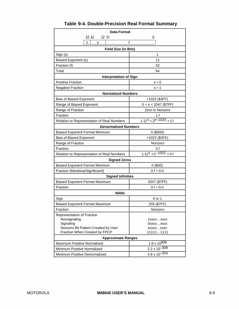
MOTOROLA M68040 USER’S MANUAL 9-9
Table 9-4. Double-Precision Real Format Summary
Data Format
s e f63 62 52 51 0
Field Size (in Bits)
Sign (s) 1
Biased Exponent (e) 11
Fraction (f) 52
Total 64
Interpretation of Sign
Positive Fraction s = 0
Negative Fraction s = 1
Normalized Numbers
Bias of Biased Exponent +1023 ($3FF)
Range of Biased Exponent 0 < e < 2047 ($7FF)
Range of Fraction Zero or Nonzero
Fraction 1.f
Relation to Representation of Real Numbers (–1)s × 2e–1023 × 1.f
Denormalized Numbers
Biased Exponent Format Minimum 0 ($000)
Bias of Biased Exponent +1022 ($3FE)
Range of Fraction Nonzero
Fraction 0.f
Relation to Representation of Real Numbers (–1)s × 2–1022 × 0.f
Signed Zeros
Biased Exponent Format Minimum 0 ($00)
Fraction (Mantissa/Significand) 0.f = 0.0
Signed Infinities
Biased Exponent Format Maximum 2047 ($7FF)
Fraction 0.f = 0.0
NANs
Sign 0 or 1
Biased Exponent Format Maximum 255 ($7FF)
Fraction Nonzero
Representation of FractionNonsignalingSignalingNonzero Bit Pattern Created by UserFraction When Created by FPCP
1xxxx…xxxx0xxxx…xxxxxxxxx…xxxx11111…1111
Approximate Ranges
Maximum Positive Normalized 1.8 x 10308
Minimum Positive Normalized 2.2 x 10–308
Minimum Positive Denormalized 4.9 x 10–324
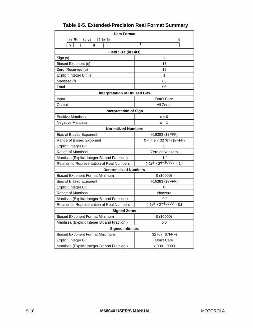
9-10 M68040 USER’S MANUAL MOTOROLA
Table 9-5. Extended-Precision Real Format Summary
Data Format
s e f95 94 80 79 64
u62 0
j63
Field Size (in Bits)
Sign (s) 1
Biased Exponent (e) 15
Zero, Reserved (u) 16
Explicit Integer Bit (j) 1
Mantissa (f) 63
Total 96
Interpretation of Unused Bits
Input Don’t Care
Output All Zeros
Interpretation of Sign
Positive Mantissa s = 0
Negative Mantissa s = 1
Normalized Numbers
Bias of Biased Exponent +16383 ($3FFF)
Range of Biased Exponent 0 < = e < 32767 ($7FFF)
Explicit Integer Bit 1
Range of Mantissa Zero or Nonzero
Mantissa (Explicit Integer Bit and Fraction ) 1.f
Relation to Representation of Real Numbers (–1)s × 2e–16383 × 1.f
Denormalized Numbers
Biased Exponent Format Minimum 0 ($0000)
Bias of Biased Exponent +16383 ($3FFF)
Explicit Integer Bit 0
Range of Mantissa Nonzero
Mantissa (Explicit Integer Bit and Fraction ) 0.f
Relation to Representation of Real Numbers (–1)s × 2–16383 × 0.f
Signed Zeros
Biased Exponent Format Minimum 0 ($0000)
Mantissa (Explicit Integer Bit and Fraction ) 0.0
Signed Infinities
Biased Exponent Format Maximum 32767 ($7FFF)
Explicit Integer Bit Don’t Care
Mantissa (Explicit Integer Bit and Fraction ) x.000…0000

MOTOROLA M68040 USER’S MANUAL 9-11
Table 9-5. Extended-Precision RealFormat Summary (Continued)
NANs
Sign Don’t Care
Explicit Integer Bit Don’t Care
Biased Exponent Format Maximum 32767 ($7FFF)
Mantissa Nonzero
Representation of MantissaNonsignalingSignalingNonzero Bit Pattern Created by UserMantissa When Created by FPCP
x.1xxxx…xxxxx.0xxxx…xxxxx.xxxxx…xxxx1.11111…1111
Approximate Ranges
Maximum Positive Normalized 1.2 × 104932
Minimum Positive Normalized 1.7 × 10–4932
Minimum Positive Denormalized 3.7 × 10–4951
Table 9-6. Packed Decimal Real Format Summary
Data Type SM SE Y Y 3-DigitExponent
1-DigitInteger
16-Digit Fraction
±Infinity 0/1 1 1 1 $FFF $XXXX $00…00
±NAN 0/1 1 1 1 $FFF $XXXX Nonzero
±SNAN 0/1 1 1 1 $FFF $XXXX Nonzero
+Zero 0 0/1 X X $000–$999 $XXX0 $00…00
–Zero 1 0/1 X X $000–$999 $XXX0 $00…00
+In-Range 0 0/1 X X $000–$999 $XXX0–$XXX9 $00…01–$99…99
–In-Range 1 0/1 X X $000–$999 $XXX0–$XXX9 $00…01–$99…99
9.4 COMPUTATIONAL ACCURACY
Whenever an attempt is made to represent a real number in a binary format of finiteprecision, there is a possibility that the number can not be represented exactly. This iscommonly referred to as a round-off error. Furthermore, when two inexact numbers areused in a calculation, the error present in each number is reflected, and possiblyaggravated, in the result. All FPU calculations use an intermediate result. When theMC68040 performs an operation, the calculation is carried out using extended-precisioninputs, and the intermediate result is calculated as if to produce infinite precision. After thecalculation is complete, the intermediate result is rounded to the selected precision andstored in the destination.
The FPCR encodings provide emulation for devices that only support single and doubleprecision. The execution speed of all instructions is the same whether using single- ordouble-precision rounding. When using these two forced rounding precisions, the

9-12 M68040 USER’S MANUAL MOTOROLA
MC68040 produces the same results as any other device that conforms to the IEEE 754standard but does not support extended precision. The results are the same whenperforming the same operation in extended precision and storing the results in single- ordouble-precision format.
The FPU performs all floating-point internal operations in extended precision. It supportsmixed-mode arithmetic by converting single- and double-precision operands to extended-precision values before performing the specified operation. The FPU converts all memorydata formats to extended-precision before using it in a floating-point operation or loading itin a floating-point data register. The FPU also converts extended-precision data formats ina floating-point data register to any data format and either stores it in a memorydestination or in an integer data register.
If the external operand is a denormalized number, the number is normalized before anoperation is performed. However, an external denormalized number moved into a floating-point data register is stored as a denormalized number.
If an external operand is an unnormalized number, the number is normalized before it isused in an arithmetic operation. If the external operand is an unnormalized zero (i.e., witha mantissa of all zeros), the number is converted to a normalized zero before the specifiedoperation is performed. The regular use of unnormalized inputs not only defeats thepurpose of the IEEE 754 standard, but also can produce gross inaccuracies in the results.
9.4.1 Intermediate Result
Figure 9-7 illustrates the intermediate result format. The intermediate result’s exponent forsome dyadic operations (i.e., multiply and divide) can easily overflow or underflow the 15-bit exponent of the destination floating-point register. To simplify the overflow andunderflow detection, intermediate results in the FPU maintain a 16-bit, twos-complementinteger exponent. Detection of an overflow or underflow intermediate result alwaysconverts the 16-bit exponent into a 15-bit biased exponent before being stored in afloating-point data register. The FPU internally maintains the 67-bit mantissa for roundingpurposes. The mantissa is always rounded to 64 bits (or less, depending on the selectedrounding precision) before it is stored in a floating-point data register.
16-BIT EXPONENT 63-BIT FRACTION
LSB OF FRACTION GUARD BITROUND BITSTICKY BIT
INTEGER BITOVERFLOW BIT
Figure 9-7. Intermediate Result Format
If the destination is a floating-point data register, the result is in the extended-precisionformat and is rounded to the precision specified by the FPSR PREC bits before beingstored. All mantissa bits beyond the selected precision are zero. If the single- or double-

MOTOROLA M68040 USER’S MANUAL 9-13
precision mode is selected, the exponent value is in the correct range even if it is stored inextended-precision format. If the destination is a memory location, the FPSR PREC bitsare ignored. In this case, a number in the extended-precision format is taken from thesource floating-point data register, rounded to the destination format precision, and thenwritten to memory.
Depending on the selected rounding mode or destination data format in effect, the locationof the least significant bit of the mantissa and the locations of the guard, round, and stickybits in the 67-bit intermediate result mantissa varies. The guard and round bits are alwayscalculated exactly. The sticky bit is used to create the illusion of an infinitely wideintermediate result. As the arrow illustrates in Figure 9-7, the sticky bit is the logical OR ofall the bits in the infinitely precise result to the right of the round bit. During the calculationstage of an arithmetic operation, any non-zero bits generated that are to the right of theround bit set the sticky bit to one. Because of the sticky bit, the rounded intermediateresult for all required IEEE arithmetic operations in the RN mode is in error by no morethan one-half unit in the last place.
9.4.2 Rounding The Result
Range control is the process of rounding the mantissa of the intermediate result to thespecified precision and checking the 16-bit intermediate exponent to ensure that it iswithin the representable range of the selected rounding-precision format. Range controlensures correct emulation of a device that only supports single- or double-precisionarithmetic. If the intermediate result’s exponent exceeds the range of the selectedprecision, the exponent value appropriate for an underflow or overflow is stored as theresult in the 16-bit extended-precision format exponent. For example, if the data formatand rounding mode is single-precision RM and the result of an arithmetic operationoverflows the magnitude of the single-precision format, the largest normalized single-precision value is stored as an extended-precision number in the destination floating-pointdata register (i.e., an unbiased 15-bit exponent of $00FF and a mantissa of$FFFFFF0000000000). If an infinity is the appropriate result for an underflow or overflow,the infinity value for the destination data format is stored as the result (i.e., an exponentwith the maximum value and a mantissa of zero).
Figure 9-8 illustrates the algorithm that is used to round an intermediate result to theselected rounding precision and destination data format. If the destination is a floating-point data register, either the selected rounding precision specified by the FPCR PRECbits or by the instruction itself determines the rounding boundary. For example, FSADDand FDADD specify single- and double-precision rounding regardless of the precisionspecified in the FPCR PREC bits. If the destination is external memory or an integer dataregister, the destination data format determines the rounding boundary. If the roundedresult of an operation is not exact, then the INEX2 bit is set in the FPSR EXC byte.

9-14 M68040 USER’S MANUAL MOTOROLA
ENTRY
INEX2 1
GUARD 0 ROUND 0 STICKY 0
EXIT EXIT
GUARD, ROUND, AND STICKY ARE
CHOPPED
SHIFT MANTISSA RIGHT 1 BIT,
ADD 1 TO EXPONENT
ADD 1 TO LSB
SELECT ROUNDING MODE
GUARD AND LSB = 1, ROUND AND STICKY = 0
OR GUARD = 1
ROUND OR STICKY = 1
INTERMEDIATE RESULT
OVERFLOW = 1
GUARD, ROUND, AND STICKY BITS = 0
EXACT RESULT
RPRMRN RZ
ADD 1 TO LSB
INTERMEDIATE RESULT
POS NEG POS NEG
Figure 9-8. Rounding Algorithm Flowchart
The three additional bits beyond the extended-precision format, the difference betweenthe intermediate result’s 67-bit mantissa and the stored result’s 64-bit mantissa, allow theFPU to perform all calculations as though it were performing calculations using a floatengine with infinite bit precision. The result is always correct for the specified destination’sdata format before performing rounding (unless an overflow or underflow error occurs).The specified rounding operation then produces a number that is as close as possible tothe infinitely precise intermediate value and still representable in the selected precision.
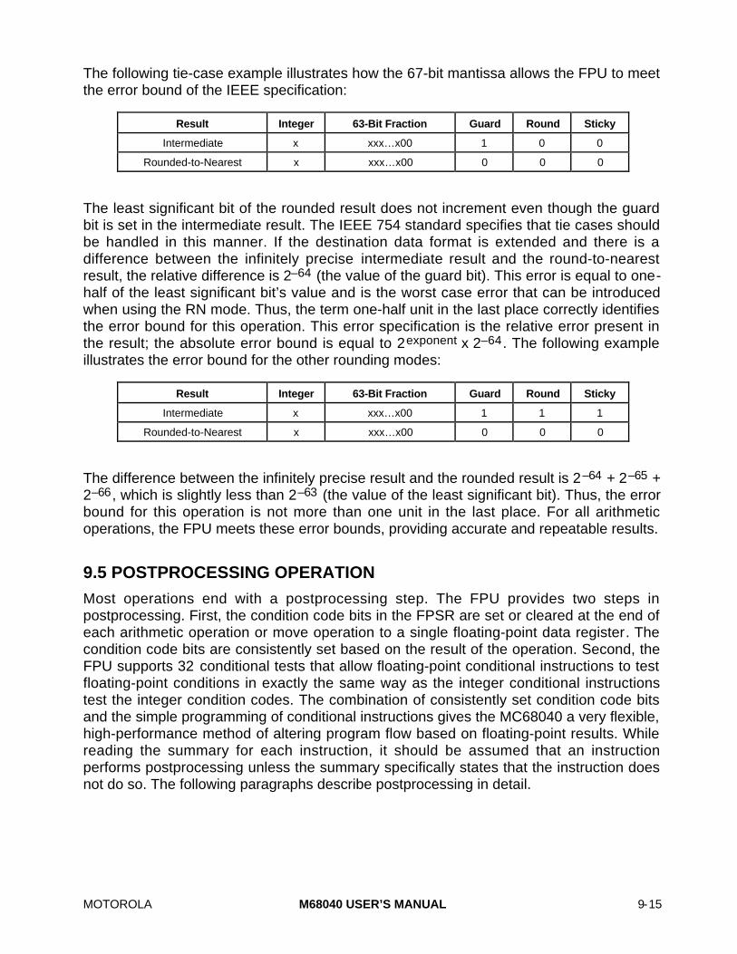
MOTOROLA M68040 USER’S MANUAL 9-15
The following tie-case example illustrates how the 67-bit mantissa allows the FPU to meetthe error bound of the IEEE specification:
Result Integer 63-Bit Fraction Guard Round Sticky
Intermediate x xxx…x00 1 0 0
Rounded-to-Nearest x xxx…x00 0 0 0
The least significant bit of the rounded result does not increment even though the guardbit is set in the intermediate result. The IEEE 754 standard specifies that tie cases shouldbe handled in this manner. If the destination data format is extended and there is adifference between the infinitely precise intermediate result and the round-to-nearestresult, the relative difference is 2–64 (the value of the guard bit). This error is equal to one-half of the least significant bit’s value and is the worst case error that can be introducedwhen using the RN mode. Thus, the term one-half unit in the last place correctly identifiesthe error bound for this operation. This error specification is the relative error present inthe result; the absolute error bound is equal to 2exponent x 2–64. The following exampleillustrates the error bound for the other rounding modes:
Result Integer 63-Bit Fraction Guard Round Sticky
Intermediate x xxx…x00 1 1 1
Rounded-to-Nearest x xxx…x00 0 0 0
The difference between the infinitely precise result and the rounded result is 2–64 + 2–65 +2–66, which is slightly less than 2–63 (the value of the least significant bit). Thus, the errorbound for this operation is not more than one unit in the last place. For all arithmeticoperations, the FPU meets these error bounds, providing accurate and repeatable results.
9.5 POSTPROCESSING OPERATION
Most operations end with a postprocessing step. The FPU provides two steps inpostprocessing. First, the condition code bits in the FPSR are set or cleared at the end ofeach arithmetic operation or move operation to a single floating-point data register. Thecondition code bits are consistently set based on the result of the operation. Second, theFPU supports 32 conditional tests that allow floating-point conditional instructions to testfloating-point conditions in exactly the same way as the integer conditional instructionstest the integer condition codes. The combination of consistently set condition code bitsand the simple programming of conditional instructions gives the MC68040 a very flexible,high-performance method of altering program flow based on floating-point results. Whilereading the summary for each instruction, it should be assumed that an instructionperforms postprocessing unless the summary specifically states that the instruction doesnot do so. The following paragraphs describe postprocessing in detail.
9-16 M68040 USER’S MANUAL MOTOROLA
9.5.1 Underflow, Round, Overflow
During the calculation of an arithmetic result, the FPU arithmetic logic unit (ALU) has moreprecision and range than the 80-bit extended-precision format. However, the final result ofthese operations is an extended-precision floating-point value. In some cases, anintermediate result becomes either smaller or larger than can be represented in extendedprecision. Also, the operation can generate a larger exponent or more bits of precisionthan can be represented in the chosen rounding precision. For these reasons, everyarithmetic instruction ends by rounding the result and checking for overflow and underflow.
At the completion of an arithmetic operation, the intermediate result is checked to see if itis too small to be represented as a normalized number in the selected precision. If so, theUNFL-bit is set in the FPSR EXC byte. The MC68040 then takes a nonmaskableunderflow exception and executes the M68040FPSP underflow exception handler,denormalizing the result. Denormalizing a number causes a loss of accuracy, but a zero isnot returned unless absolutely necessary. If a number has grossly underflowed, theM68040FPSP returns a zero or the smallest denormalized number with the correct sign,depending on the rounding mode in effect.
If no underflow occurs, the intermediate result is rounded according to the user-selectedrounding precision and rounding mode. After rounding, the INEX2-bit of the FPSR EXCbyte is set accordingly. Finally, the magnitude of the result is checked to see if it is toolarge to be represented in the current rounding precision. If so, the OVFL-bit of the FPSREXC byte is set. The M68040FPSP returns a correctly signed infinity or a correctly signedlargest normalized number, depending on the rounding mode in effect.
9.5.2 Conditional Testing
Unlike the integer arithmetic condition codes, an instruction either always sets the floating-point condition codes in the same way or it does not change them at all. Therefore, theinstruction descriptions do not include floating-point condition code settings. The followingparagraphs describe how floating-point condition codes are set for all instructions thatmodify condition codes. Refer to 9.2.3.1 Floating-Point Condition Code Byte for adescription of the FPCC byte.
The condition code bits differ slightly from the integer condition codes. Unlike theoperation-type-dependent integer condition codes, examining the result at the end of theoperation sets or clears the floating-point condition codes accordingly. The M68000 familyinteger condition codes bits N and Z have this characteristic, but the V and C bits are setdifferently for different instructions. The data type of the operation’s result determines howthe four condition code bits are set. Table 9-7 lists the condition code bit setting for eachdata type. The MC68040 generates only eight of the 16 possible combinations. Loadingthe FPCC with one of the other combinations and executing a conditional instruction canproduce an unexpected branch condition.
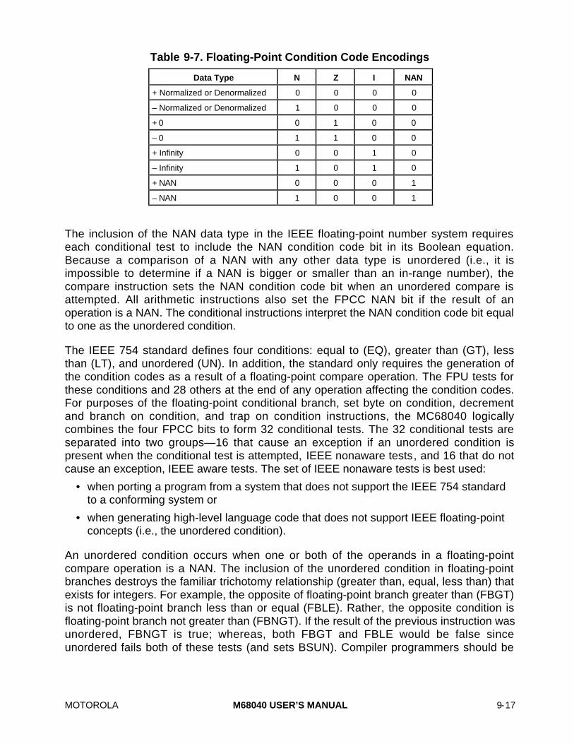
MOTOROLA M68040 USER’S MANUAL 9-17
Table 9-7. Floating-Point Condition Code Encodings
Data Type N Z I NAN
+ Normalized or Denormalized 0 0 0 0
– Normalized or Denormalized 1 0 0 0
+ 0 0 1 0 0
– 0 1 1 0 0
+ Infinity 0 0 1 0
– Infinity 1 0 1 0
+ NAN 0 0 0 1
– NAN 1 0 0 1
The inclusion of the NAN data type in the IEEE floating-point number system requireseach conditional test to include the NAN condition code bit in its Boolean equation.Because a comparison of a NAN with any other data type is unordered (i.e., it isimpossible to determine if a NAN is bigger or smaller than an in-range number), thecompare instruction sets the NAN condition code bit when an unordered compare isattempted. All arithmetic instructions also set the FPCC NAN bit if the result of anoperation is a NAN. The conditional instructions interpret the NAN condition code bit equalto one as the unordered condition.
The IEEE 754 standard defines four conditions: equal to (EQ), greater than (GT), lessthan (LT), and unordered (UN). In addition, the standard only requires the generation ofthe condition codes as a result of a floating-point compare operation. The FPU tests forthese conditions and 28 others at the end of any operation affecting the condition codes.For purposes of the floating-point conditional branch, set byte on condition, decrementand branch on condition, and trap on condition instructions, the MC68040 logicallycombines the four FPCC bits to form 32 conditional tests. The 32 conditional tests areseparated into two groups—16 that cause an exception if an unordered condition ispresent when the conditional test is attempted, IEEE nonaware tests, and 16 that do notcause an exception, IEEE aware tests. The set of IEEE nonaware tests is best used:
• when porting a program from a system that does not support the IEEE 754 standardto a conforming system or
• when generating high-level language code that does not support IEEE floating-pointconcepts (i.e., the unordered condition).
An unordered condition occurs when one or both of the operands in a floating-pointcompare operation is a NAN. The inclusion of the unordered condition in floating-pointbranches destroys the familiar trichotomy relationship (greater than, equal, less than) thatexists for integers. For example, the opposite of floating-point branch greater than (FBGT)is not floating-point branch less than or equal (FBLE). Rather, the opposite condition isfloating-point branch not greater than (FBNGT). If the result of the previous instruction wasunordered, FBNGT is true; whereas, both FBGT and FBLE would be false sinceunordered fails both of these tests (and sets BSUN). Compiler programmers should be

9-18 M68040 USER’S MANUAL MOTOROLA
particularly careful of the lack of trichotomy in the floating-point branches since it iscommon for compilers to invert the sense of conditions.
When using the IEEE nonaware tests, the user receives a BSUN exception whenever abranch is attempted and the NAN condition code bit is set, unless the branch is an FBEQor an FBNE. If the BSUN exception is enabled in the FPCR, the exception causes anotherexception. Therefore, the IEEE nonaware program is interrupted if an unexpectedcondition occurs. Compilers and programmers who are knowledgeable of the IEEE 754standard should use the IEEE aware tests in programs that contain ordered andunordered conditions. Since the ordered or unordered attribute is explicitly included in theconditional test, the BSUN bit is not set in the FPSR EXC byte when the unorderedcondition occurs. Table 9-8 summarizes the conditional mnemonics, definitions,equations, predicates, and whether the BSUN bit is set in the FPSR EXC byte for the 32floating-point conditional tests. The equation column lists the combination of FPCC bits foreach test in the form of an equation.
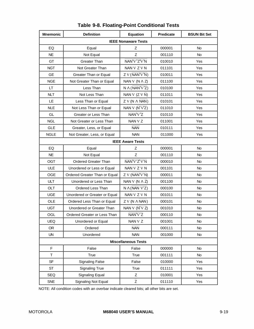
MOTOROLA M68040 USER’S MANUAL 9-19
Table 9-8. Floating-Point Conditional Tests
Mnemonic Definition Equation Predicate BSUN Bit Set
IEEE Nonaware Tests
EQ Equal Z 000001 No
NE Not Equal Z 001110 No
GT Greater Than NAN V Z V N 010010 Yes
NGT Not Greater Than NAN V Z V N 011101 Yes
GE Greater Than or Equal Z V (NAN V N) 010011 Yes
NGE Not Greater Than or Equal NAN V (N Λ Z) 011100 Yes
LT Less Than N Λ (NAN V Z) 010100 Yes
NLT Not Less Than NAN V (Z V N) 011011 Yes
LE Less Than or Equal Z V (N Λ NAN) 010101 Yes
NLE Not Less Than or Equal NAN V (N V Z) 011010 Yes
GL Greater or Less Than NAN V Z 010110 Yes
NGL Not Greater or Less Than NAN V Z 011001 Yes
GLE Greater, Less, or Equal NAN 010111 Yes
NGLE Not Greater, Less, or Equal NAN 011000 Yes
IEEE Aware Tests
EQ Equal Z 000001 No
NE Not Equal Z 001110 No
OGT Ordered Greater Than NAN V Z V N 000010 No
ULE Unordered or Less or Equal NAN V Z V N 001101 No
OGE Ordered Greater Than or Equal Z V (NAN V N) 000011 No
ULT Unordered or Less Than NAN V (N Λ Z) 001100 No
OLT Ordered Less Than N Λ (NAN V Z) 000100 No
UGE Unordered or Greater or Equal NAN V Z V N 001011 No
OLE Ordered Less Than or Equal Z V (N Λ NAN) 000101 No
UGT Unordered or Greater Than NAN V (N V Z) 001010 No
OGL Ordered Greater or Less Than NAN V Z 000110 No
UEQ Unordered or Equal NAN V Z 001001 No
OR Ordered NAN 000111 No
UN Unordered NAN 001000 No
Miscellaneous Tests
F False False 000000 No
T True True 001111 No
SF Signaling False False 010000 Yes
ST Signaling True True 011111 Yes
SEQ Signaling Equal Z 010001 Yes
SNE Signaling Not Equal Z 011110 Yes
NOTE: All condition codes with an overbar indicate cleared bits; all other bits are set.

9-20 M68040 USER’S MANUAL MOTOROLA
9.6 FLOATING-POINT EXCEPTIONS
There are two classes of floating-point-related exceptions: nonarithmetic floating-pointexceptions and arithmetic floating-point exceptions. The latter relates to the handling ofarithmetic exceptions caused by floating-point activity, and the former includesunimplemented floating-point instructions and unsupported data types not related to thehandling of arithmetic exceptions. Format error and FTRAPcc exceptions may seem to befloating-point related, but are considered IU exceptions (see Section 8 ExceptionProcessing). The following sections detail floating-point exceptions and how theMC68040 and M68040FPSP handle them. Table 9-9 lists the vector numbers related tofloating-point exceptions.
Table 9-9. Floating-Point Exception Vectors
VectorNumber
Vector Offset(Hex)
Assignment
11
48495051
02C
0C00C40C80CC
Floating-Point Unimplemented Instruction(also used for F-line instruction)
Floating-Point Branch or Set on Unordered ConditionFloating-Point Inexact ResultFloating-Point Divide by ZeroFloating-Point Underflow
52535455
0D00D40D80DC
Floating-Point Operand ErrorFloating-Point OverflowFloating-Point SNANFloating-Point Unimplemented Data Type
The following paragraphs detail nonarithmetic floating-point exceptions.
9.6.1 Unimplemented Floating-Point Instructions
F-line instructions are instruction word patterns with bits 15–12 that have an $F encoding,causing F-line exceptions. These instructions are termed unimplemented floating-pointinstructions and cause an unimplemented floating-point exception. The MC68040recognizes some F-line instructions, such as the FMUL and CPUSH, which do not causeF-line exceptions. There are some F-line instructions that the MC68040 recognizes asvalid MC68881/MC68882 floating-point instruction patterns, but as floating-pointinstructions that the processor cannot complete in hardware. Table 9-10 lists the floating-point instructions that are unimplemented and therefore cause an unimplementedinstruction exception.
If the processor encounters an F-line instruction and the instruction patterns do not matcheither of the above two cases, the processor takes an F-line illegal exception. F-line illegalexceptions are discussed further in Section 8 Exception Processing. The processorgenerates an exception with vector number 11 and pushes a four-word stack frame format$0 on the system stack. An illegal instruction exception is also reported when a breakpointacknowledge bus cycle is run and terminated with either a transfer acknowledge (TA) ortransfer error acknowledge (TEA) signal. Since the unimplemented floating-point

MOTOROLA M68040 USER’S MANUAL 9-21
exception and the F-line illegal instruction share the same vector, the exception handleruses the stack frame format ($0 or $2) to distinguish between the two.
Table 9-10. Unimplemented Instructions
Monadic Operations
FACOS FINTRZ
FASIN FLOG10
FATAN FLOGN
FATANH FLOGNP1
FCOS FMOVECR
FCOSH FSIN
FETOX FSINCOS
FETOXM1 FSINH
FGETEXP FTAN
FGETMAN FTANH
FINT FTENTOX
FTWOTOX —
Dyadic Operations
FMOD FREM
FSCALE —
When an unimplemented floating-point instruction is encountered, the processor waits forall previous floating-point instructions to complete execution. Pending exceptions aretaken and handled prior to the execution of the unimplemented instruction.
Next, the instruction is partially decoded to allow fetching of the memory source operand,if required. When the operand fetch begins, all other read accesses for previousinstructions are complete, and only the execution and write-back of results for previousinteger instructions remains to be completed. If an access error (bus error) occurs infetching the operand or in completing any other access before beginning the operandfetch, the unimplemented instruction is restarted after the processor returns fromexception handling for the error. Refer to Section 8 Exception Processing for moreinformation on access errors.
The fetched source operand is passed to the FPU, which converts the operand toextended precision and saves the intermediate result. If the operand is an unsupporteddata type (denormalized, unnormalized, or packed decimal real), the unimplementedfloating-point exception takes precedence, and the floating-point instruction emulationroutine must detect the unsupported data type.
The processor begins exception processing for the unimplemented floating-pointinstruction by making an internal copy of the current SR. The processor then enters thesupervisor mode and clears the trace bits (T1, T0). The processor creates a format $2stack frame and saves the vector offset, PC, internal copy of the SR, and calculated

9-22 M68040 USER’S MANUAL MOTOROLA
effective address in the stack frame. The saved PC value is the logical address of theinstruction that follows the unimplemented floating-point instruction. The processorgenerates exception vector number 11 for the unimplemented F-line instruction exceptionvector, fetches the address of the F-line exception handler from the processor’s exceptionvector table, pushes the format $2 stack frame on the system stack, and begins executionof the exception handler after prefetching instructions to fill the pipeline. The exceptionhandler emulates the unimplemented floating-point instruction in software, maintaininguser-object-code compatibility. Refer to Section 8 Exception Processing for detailsabout exception vectors and format $2 stack frames.
The F-line exception handler checks for the format $2 stack frame to distinguish anunimplemented floating-point instruction from other F-line unimplemented instructions.When the exception handler for unimplemented floating-point instructions executes anFSAVE, a 26-word unimplemented instruction state frame is created (see Figure 9-10). Atthis point, an FSAVE instruction yields the information as listed in Table 9-16. Note thatunless the instruction specifies a packed decimal real source, the state frame containsboth operands (if required). For packed decimal real data format, the second operand is inthe designated format of the destination floating-point data register.
The exception handler uses the information provided in the state frame to determine theinstruction that it needs to emulate and the input operands to that instruction. Once theinstruction has been emulated and the result is reached, the exception handler moves theresult into the appropriate destination floating-point data register, discards theunimplemented instruction state frame, and returns to normal instruction flow using theRTE instruction. The limitation to this approach is that no floating-point arithmeticexceptions can be reported at the end of the emulated instruction.
The M68040FPSP not only emulates the instruction, but in addition, it ensures that if anyfloating-point arithmetic exceptional conditions arise from the emulation of theunimplemented instruction and if the corresponding floating-point arithmetic exception isenabled, the M68040FPSP manipulates the stack and restores the stack back into theFPU in the desired exceptional state. This effectively imitates the action of the MC68040implemented instructions since the exception is not reported until the next floating-pointinstruction is encountered. This manipulation of the stack is rather complicated and isbeyond the scope of this manual. Motorola recommends that the user utilize theM68040FPSP if a full exception-reporting model is required. Motorola does not provideany printed documentation other than what is embedded in the source code of theM68040FPSP.
9.6.2 Unsupported Floating-Point Data Types
An unsupported data type exception occurs when either operand to an implementedfloating-point instruction is denormalized (for single-, double-, and extended-precisionoperands), unnormalized (for extended-precision operands), or either the source ordestination data format is packed decimal real. These data types are unimplemented inthe MC68040 and must be emulated in software.

MOTOROLA M68040 USER’S MANUAL 9-23
NOTE
In this manual, all references to the unsupported floating-pointdata types also refer to the unimplemented data types in theM68040FPSP.
When the processor encounters an unsupported data type, the procedure taken isidentical to that used when an unimplemented instruction is taken. Unsupported datatypes with operands that have opclass 010 or 000 (register-to-register or memory-to-register) instructions cause a pre-instruction exception. When an unsupported data type isdetected for opclass 011 (register-to-memory) instructions, a post-instruction exception isgenerated immediately. A format $0 (for the pre-instruction exception) or format $3 (for thepost-instruction exception) stack frame is saved, and vector number 55 is fetched. Adenormalized value generated as the result of a floating-point operation generates anonmaskable underflow exception instead of an unsupported data type exception.
Table 9-16 lists the floating-point state frame fields for unsupported data type exceptionsresulting from the execution of opclass 010 or 000 (register-to-register or memory-to-register) instructions, and opclass 011 (register-to-memory) instructions defined for theuse by the supervisor exception handler.
A denormalized or unnormalized extended-precision source or destination operand iscopied directly without modification to ETEMP or FPTEMP fields in the floating-point stateframe. If a packed decimal real source operand is specified, the upper 32 bits of theoperand are copied to the FPTEMP field, and the lower 64 bits are copied to ETEMP. Thedestination operand in this case remains in the destination floating-point register, and canbe either denormalized or unnormalized. Figure 9-9 illustrates denormalized single- (a)and double-precision (b) operands stored in ETEMP field.
The exception handler uses the floating-point state frame information to determine whichoperand (or operands) is the unsupported data type and which instruction attempted touse the offending operand. The exception handler must provide the routines needed tocomplete the instruction and to store that instruction to the proper destination, whether itbe in a floating-point data register, integer data register, or external memory. Once thedestination is written, the floating-point state frame is discarded, and normal execution isresumed by using the RTE instruction. This approach does not report floating-pointarithmetic exceptions that may have been generated. Motorola recommends that the userutilize the M68040FPSP if a full exception-reporting model is required. Motorola does notprovide any printed documentation other than what is embedded in the source code of theM68040FPSP.

9-24 M68040 USER’S MANUAL MOTOROLA
DENORMALIZED SINGLE PRECISION
31 30 23 22 0
0394062636479809495
$0S
$0 $0 $00FORMAT IN STATE FRAME
MANTISSAEXPS
FRACTION
DENORMALIZED DOUBLE PRECISION
63 62 52 51 0
0101162636479809495
$0S
$0 $0 $00FORMAT IN STATE FRAME
MANTISSAEXPS
MANTISSA
(a) Single Precision
(b) Double Precision
Figure 9-9. Format of Denormalized Operand in State Frame
9.7 FLOATING-POINT ARITHMETIC EXCEPTIONS
The following eight user floating-point arithmetic exceptions are listed in order of priority.The MC68040 generates the first seven exceptions in hardware and the eighth only insoftware.
• Branch/Set on Unordered (BSUN)
• Signaling Not-A-Number (SNAN)
• Operand Error (OPERR)
• Overflow (OVFL)
• Underflow (UNFL)
• Divide by Zero (DZ)
• Inexact 2 (INEX2)
• Inexact 1 (INEX1)
INEX1 exception is the condition that exists when a packed decimal operand cannot beconverted exactly to the extended-precision format in the current rounding mode. Since

MOTOROLA M68040 USER’S MANUAL 9-25
the MC68040 does not directly support packed decimal real operands, the processornever sets INEX1 bit in the FPSR EXC byte, but provides it as a latch so that emulationsoftware can report the exception.
A floating-point arithmetic exception is taken in one of two situations. The first situationoccurs when the user program enables an arithmetic exception by setting a bit in theFPCR ENABLE byte and the corresponding bit in the FPSR EXC byte matches the bit inthe FPCR ENABLE byte as a result of program execution; this is referred to as maskableexception conditions. A user write operation to the FPSR, which sets a bit in the EXC byte,does not cause an exception to be taken, regardless of the value in the ENABLE byte.When a user writes to the ENABLE byte that enables a class of floating-point exceptions,a previously generated floating-point exception does not cause an exception to be taken,regardless of the value in the FPSR EXC byte. The user can clear a bit in the FPCRENABLE byte, disabling each corresponding exception.
The second situation occurs when the processor encounters a nonmaskable SNAN,OPERR, OVFL, and UNFL condition; this is referred to as nonmaskable exceptionconditions. This allows a supervisor exception handler to correct a defaulting resultgenerated by the MC68040 that is different from the result generated by anMC68881/MC68882 executing the same code. After correcting the result, the supervisorexception handler calls a user-defined exception handler if the exception has beenenabled in the FPCR ENABLE byte or returns to the main program flow if the exception isdisabled.
A single instruction execution can generate dual and triple exceptions. When multipleexceptions occur with exceptions enabled for more than one exception class, the highestpriority exception is reported; the lower priority exceptions are never reported or taken.The previous list of arithmetic floating-point exceptions is in order of priority. The bits ofthe ENABLE byte are organized in decreasing priority, with bit 15 being the highest and bit8 the lowest. The exception handler must check for multiple exceptions. The address ofthe exception handler is derived from the vector number corresponding to the exception.The following is a list of multiple instruction exceptions that can occur:
• SNAN and INEX1
• OPERR and INEX2
• OPERR and INEX1
• OVFL and INEX2 and/or INEX1
• UNFL and INEX2 and/or INEX1
9.7.1 Branch/Set On Unordered (BSUN)
The BSUN exception is the result of performing an IEEE nonaware conditional testassociated with the FBcc, FDBcc, FTRAPcc, and FScc instructions when an unorderedcondition is present. Refer to 9.5.2 Conditional Testing for information on conditionaltests.
9-26 M68040 USER’S MANUAL MOTOROLA
If a floating-point exception is pending from a previous floating-point instruction, a pre-instruction exception is taken. After the appropriate exception handler is executed, theconditional instruction is restarted. When the FPU pipeline is idle (all previous floating-point instructions have completed) and no exceptions are pending, the processorevaluates the conditional predicate and checks for a BSUN exception before executing theconditional instruction.
9.7.1.1 MASKABLE EXCEPTION CONDITIONS. A BSUN exception occurs if theconditional predicate is one of the IEEE nonaware branches and the FPCC NAN bit is set.When the processor detects this condition, it sets the BSUN bit in the FPSR EXC byte.
a. If the user BSUN exception handler is disabled, the floating-point condition isevaluated as if it were the equivalent IEEE aware conditional predicate. Noexceptions are taken.
b. If the user BSUN exception handler is enabled, the processor takes a floating-pointpre-instruction exception. A $0 stack frame is saved, and vector number 48 isgenerated to access the BSUN exception vector. The BSUN entry in the processor’svector table points to the M68040FPSP BSUN exception handler.
For MC68881/MC68882 compatibility, the M68040FPSP updates the FPIAR by copyingthe PC value in the pre-instruction stack frame to the FPIAR. The M68040FPSP BSUNexception handler restores the FPU to its exceptional state, cleans up the stack to thestate prior to the M68040FPSP BSUN exception handler’s execution, and continuesinstruction execution at the user BSUN exception handler. No parameters are passed tothe user BSUN exception handler since the M68040FPSP BSUN exception handlerprovides the illusion that it never existed.
The user BSUN exception handler must execute an FSAVE as its first floating-pointinstruction. FSAVE allows other floating-point instructions to execute without reporting theBSUN exception again, although none of the state frame values are useful in theexecution of the user BSUN exception handler. The BSUN exception is unique in that theexception is taken before the conditional predicate is evaluated. If the user BSUNexception handler does not set the PC to the instruction following the one that causedBSUN exception when returning, the exception is executed again. Therefore, it is theresponsibility of the user BSUN exception handler to prevent the conditional instructionfrom taking the BSUN exception again. There are four ways to prevent taking theexception again:
1. Incrementing the stored PC in the stack bypasses the conditional instruction. Thistechnique applies to situations where a fall-through is desired. Note that accuratecalculation of the PC increment requires detailed knowledge of the size of theconditional instruction being bypassed.
2. Clearing the NAN bit prevents the exception from being taken again. However, thisalone cannot deterministically control the result’s indication (true or false) that wouldbe returned when the conditional instruction reexecutes.
3. Disabling the BSUN bit also prevents the exception from being taken again. Like thesecond method, this method cannot control the result indication (true or false) thatwould be returned when the conditional instruction reexecutes.

MOTOROLA M68040 USER’S MANUAL 9-27
4. Examining the conditional predicate and setting the FPCC NAN bit accordinglyprevents the exception from being taken again. This technique gives the mostcontrol since it is possible to pre-determine the direction of program flow. Bit 7 of theF-line operation word indicates where the conditional predicate is located. If bit 7 isset, the conditional predicate is the lower six bits of the F-line operation word.Otherwise, the conditional predicate is the lower six bits of the instruction word,which immediately follows the F-line operation word. Using the conditional predicateand the table for IEEE nonaware test in 9.5.2 Conditional Testing, the conditioncodes can be set to return a known result indication when the conditional instructionis reexecuted.
Prior to exiting the user BSUN exception handler, the exception handler discards thefloating-point state frame.
9.7.1.2 NONMASKABLE EXCEPTION CONDITIONS. There are no conditions.
9.7.2 Signaling Not-a-Number (SNAN)
An SNAN is used as an escape mechanism for a user-defined, non-IEEE data type. Theprocessor never creates an SNAN as a result of an operation; a NAN created by anoperand error exception is always a nonsignaling NAN. When an operand is an SNANinvolved in an arithmetic instruction, the SNAN bit is set in the FPSR EXC byte. Since theFMOVEM, FMOVE FPCR, and FSAVE instructions do not modify the status bits, theycannot generate exceptions. Therefore, these instructions are useful for manipulatingSNANs.
9.7.2.1 MASKABLE EXCEPTION CONDITIONS. When an SNAN is encountered, if thedestination is a floating-point data register or is in memory (or an integer data register) andthe format is single, double, or extended precision, the SNAN is maskable and may ormay not take an exception.
a. If the user SNAN exception is disabled, the processor clears the SNAN bit in theNAN data format and the resulting nonsignaling NAN is transferred to thedestination. No bits other than the SNAN bit of the NAN data format are modified,although the input NAN is truncated if necessary. Instruction execution continueswithout taking any exceptions.
b. If the user SNAN exception handler is enabled, the processor posts an exceptionand another floating-point instruction is eventually encountered; a pre-instructionexception is reported at that time. The SNAN entry in the processor’s vector tablepoints to the M68040FPSP SNAN exception handler. Once the M68040FPSP SNANexception handler recognizes the operand error as a maskable condition, it does notmodify the destination or pass control to the user SNAN exception handler.
9.7.2.2 NONMASKABLE EXCEPTION CONDITIONS. When an SNAN is encountered, ifthe destination is either in memory or an integer data register and the format is byte, word,or long word, a nonmaskable post-instruction exception occurs and is taken immediately.The SNAN entry in the processor’s vector table points to the M68040FPSP SNANexception handler.

9-28 M68040 USER’S MANUAL MOTOROLA
The M68040FPSP SNAN exception handler checks to see if the instruction is an FMOVEto byte, word, or long word. If one of these conditions is met, the M68040FPSP SNANexception handler stores the most significant 8, 16, or 32 bits, respectively, of the SNANmantissa, with the SNAN bit set, to the destination. Next, it determines whether or not theuser SNAN exception is enabled.
a. If the user SNAN exception is disabled, the M68040FPSP SNAN exception handlerchecks for an INEX1 or INEX2 exception condition and determines whether or not itneeds to go to the user INEX exception handler. If not, the M68040FPSP returns tonormal instruction execution. Otherwise, the M68040FPSP SNAN exception handlerrestores the FPU to its exceptional state, cleans up the stack to the conditions priorto execution, and continues instruction execution at the user INEX exceptionhandler. No parameters are passed to the user INEX exception handler since theM68040FPSP SNAN exception handler provides the illusion that it never existed.
b. If the user SNAN exception handler is enabled, the M68040FPSP SNAN exceptionhandler checks to see if the destination is a floating-point data register or in memory(or an integer data register) with single-, double-, or extended-precision format. If so,the M68040FPSP SNAN exception handler determines which input operand is theSNAN, sets the SNAN bit in the NAN data format, and transfers the resultingnonsignaling NAN to the destination. Once the destination has been written, theM68040FPSP SNAN exception handler restores the FPU to its exceptional state,cleans up the stack to the conditions prior to its execution, and continues instructionexecution at the user SNAN exception handler. No parameters are passed to theuser SNAN exception handler since the M68040FPSP SNAN exception handlerprovides the illusion that it never existed.
The user SNAN exception handler must execute an FSAVE as the first floating-pointinstruction. Table 9-16 lists the floating-point state frame fields for SNAN pre-instructionexceptions resulting from the execution of opclass 010 or 000 (register-to-register ormemory-to-register) instructions, and for SNAN post-instruction exceptions resulting fromthe execution of opclass 011 (register-to-memory) instructions defined for the use by thesupervisor exception handler. A source or destination SNAN is stored in ETEMP orFPTEMP, respectively, with its SNAN bit set.
The user SNAN exception handler can overwrite the result to the specified destination.The exception handler must be aware that it is possible for an INEX1 exceptionalcondition to co-exist with an SNAN exception. Since the SNAN exception has higherpriority, the INEX1 exception is hidden, and it becomes the responsibility of the SNANexception handler to detect and correct this if desired. To return to normal execution, thestate frame is discarded prior to execution of the RTE of the user-defined exceptionhandler.
9.7.3 Operand Error
The operand error exception encompasses problems arising in a variety of operations,including those errors not frequent or important enough to merit a specific exceptionalcondition. Basically, an operand error occurs when an operation has no mathematicalinterpretation for the given operands. Table 9-11 lists the possible operand errors, bothnative and not native to the MC68040, which the M68040FPSP unimplemented instruction

MOTOROLA M68040 USER’S MANUAL 9-29
exception handler can report. When an operand error occurs, the OPERR bit is set in theFPSR EXC byte.
Table 9-11. Possible Operand Errors Exceptions
Instruction Condition Causing Operand Error
Native to MC68040
FADD (+inf) + (–inf) or (–inf) + (+inf)
FDIV 0 ÷ 0 or inf ÷ inf
FMOVE to B,W,or L Integer overflow where the source is nonsignaling NAN or +infinity.
FMUL One operand is 0 and other is +inf.
FSQRT Source < 0 or ±inf.
FSUB (+inf) – (+inf) or (–inf) – (–inf)
Nonnative to MC68040
FACOS Source is ±inf, > +1, or < –1
FASIN Source is ±inf, > +1, or < –1
FATANH Source is > +1 or < –1
FCOS Source is ±inf
FGETEXP Source is ±inf
FGETMAN Source is ±inf
FLOG10 Source is < 0
FLOG2 Source is < 0
FLOGN Source is < 0
FLOGNP1 Source is ≤ 1
FMOD Floating-point data register is ±inf or source is 0, other operand is not a NAN
FMOVE to P Source exponent > 999 (decimal) or k-Factor > 17
FREM Floating-point data register is ±inf or source is 0, other operand is not a NAN
FSCALE Source is ±inf
FSGLDIV 0 ÷ 0 or inf ÷ inf
FSGLMUL One operand is 0, other operand is inf
FSIN Source is ±inf
FSINCOS Source is ±inf
FTAN Source is ±inf
9.7.3.1 MASKABLE EXCEPTION CONDITIONS. All conditions apply as listed in Table9-11, with the exception of the FMOVE to byte, word, or long-word case.
a. If the user OPERR exception handler is disabled, an extended-precisionnonsignaling NAN with all mantissa bits set is stored in the destination floating-pointdata register. No exceptions are reported, and instruction execution proceedsnormally.

9-30 M68040 USER’S MANUAL MOTOROLA
b. If the user OPERR exception handler is enabled and the destination floating-pointdata register is not modified, an OPERR exception is posted. The next floating-pointinstruction that is encountered takes a pre-instruction exception. The OPERR entryin the processor’s vector table points to the M68040FPSP OPERR exceptionhandler. Once the M68040FPSP OPERR exception handler recognizes the operanderror as a maskable condition, it does not modify the destination or pass control tothe user OPERR exception handler.
9.7.3.2 NONMASKABLE EXCEPTION CONDITIONS. If an FMOVE to byte, word, or longword has a source operand that is too large to be represented in the specified destinationinteger format (integer overflow, NAN, infinity) or if the source operand is equal to thelargest negative integer representable in the specified destination integer format(erroneous MC68040 condition), the processor immediately takes a post-instructionexception. Instruction execution continues at the M68040FPSP OPERR exceptionhandler.
If the M68040FPSP determines a nonmaskable erroneous MC68040 condition caused theexception, it stores the largest negative integer representable in the given destinationinteger format (–27 for byte, –215 for word, and –231 for long word). The M68040FPSPOPERR exception handler then returns the processor to normal processing. If an integeroverflow or an FMOVE to byte, word, or long word with a source of infinity causes theexception, then the destination is written with the largest positive or negative integer thatcan be represented in the given format. If an FMOVE to byte of word or long word with asource of NAN causes the exception, then the most significant 8, 16, or 32 bits,respectively, are written to the destination. Next, the M68040FPSP OPERR exceptionhandler checks to see if the user OPERR exception handler is enabled.
a. If the user OPERR exception handler is disabled, an exception-causing INEX1 orINEX2 condition exists, and the user INEX exception handler is enabled. TheM68040FPSP OPERR exception handler restores the FPU to its exceptional state,cleans up the stack to the conditions prior to execution, and continues instructionexecution at the user INEX exception handler. No parameters are passed to the userINEX exception handler since the M68040FPSP OPERR exception handler providesthe illusion that it never existed. Otherwise, the M68040FPSP OPERR exceptionhandler returns the processor to normal processing.
b. If the user OPERR exception handler is enabled and the destination is a floating-point data register, then the M68040FPSP exception handler does not modify theregister. The M68040FPSP OPERR exception handler restores the FPU to itsexceptional state, cleans up the stack to the conditions prior to execution, andcontinues instruction execution at the user OPERR exception handler. Noparameters are passed to the user OPERR exception handler since theM68040FPSP OPERR exception handler provides the illusion that it never existed.
The user OPERR exception handler must execute an FSAVE as its first floating-pointinstruction. Table 9-16 lists the floating-point state frame fields for OPERR exceptionsresulting from the execution of opclass 010 or 000 (register-to-register or memory-to-register) instructions and opclass 011 (register-to-memory) instructions defined for the useby the supervisor exception handler.
MOTOROLA M68040 USER’S MANUAL 9-31
The CMDREG1B field of the floating-point state frame can be used to determine theinstruction that caused of the OPERR exception. Note that CMDREG1B could be any ofthe instructions listed in Table 9-11. If the destination is a floating-point data register, thisexception handler needs to supply the contents. If the destination is memory, the effectiveaddress is supplied in the format $3 stack frame. If the destination is an integer dataregister, the FPIAR points to the F-line instruction word that contains the integer dataregister number. To exit the user OPERR exception handler, the saved floating-pointframe need not be restored and can be discarded prior to execution of the RTEinstruction.
9.7.4 Overflow
An overflow exception is detected for arithmetic operations in which the destination is afloating-point data register or memory when the intermediate result’s exponent is greaterthan or equal to the maximum exponent value of the selected rounding precision.Overflow can only occur when the destination is in the single-, double-, or extended-precision format; all other data format overflows are handled as operand errors. At the endof any operation that could potentially overflow, the intermediate result is checked forunderflow, rounded, and then checked for overflow before it is stored to the destination. Ifoverflow occurs, the OVFL bit is set in the FPSR EXC byte.
Even if the intermediate result is small enough to be represented as an extended-precision number, an overflow can occur. The intermediate result is rounded to theselected precision, and the rounded result is stored in the extended-precision format. If themagnitude of the intermediate result exceeds the range of the selected rounding precisionformat, an overflow occurs.
9.7.4.1 MASKABLE EXCEPTION CONDITIONS. There are no conditions.
9.7.4.2 NONMASKABLE EXCEPTION CONDITIONS. When the OVFL bit is set in theFPSR EXC byte as a result of a floating-point instruction, the processor always takes anonmaskable overflow exception. If the destination is a floating-point data register, thenthe register is not affected, and either a pre-instruction or a post-instruction exception isreported. If the destination is a memory or integer data register, an undefined result isstored, and a post-instruction exception is taken immediately. Execution begins at theM68040FPSP OVFL exception handler.
The values defined in Table 9-12 are stored in the destination based on the roundingmode defined in the FPCR MODE byte. The M68040FPSP OVFL exception handlerrounds the result according to the rounding precision defined in the FPCR MODE byte ifthe destination is a floating-point data register. If the destination is in memory or an integerdata register, then the rounding precision in the FPCR MODE byte is ignored, and thegiven destination format defines the rounding precision. If the instruction has a forcedrounding precision (e.g., FSADD, FDMUL), the instruction defines the rounding precision.The M68040FPSP OVFL exception handler then checks to see if the user OVFLexception handler is enabled.

9-32 M68040 USER’S MANUAL MOTOROLA
Table 9-12. Overflow Rounding Mode Values
RoundingMode
Result
RN Infinity, with the sign of the intermediate result.
RZ Largest magnitude number, with the sign of the intermediate result.
RM For positive overflow, largest positive number; for negative overflow, infinity.
RP For positive overflow, infinity; for negative overflow, largest negative number.
a. If the user OVFL exception handler is disabled, the M68040FPSP OVFL exceptionhandler checks for an INEX1 or INEX2 exception condition with the user INEXexception handler enabled. If not, the processor returns to normal instruction flow.Otherwise, the M68040FPSP OVFL exception handler restores the FPU to itsexceptional state, cleans up the stack to the conditions prior its execution, andcontinues instruction execution at the user INEX exception handler. No parametersare passed to the user INEX exception handler since the M68040FPSP OVFLexception handler provides the illusion that it never existed. Otherwise, theM68040FPSP OVFL exception handler returns the processor to normal processing.
b. If the user OVFL exception handler is enabled, the M68040FPSP OVFL restores theFPU to its exceptional state, cleans up the stack to the conditions prior to execution,and continues instruction execution at the user OVFL exception handler. Noparameters are passed to the user OVFL exception handler since the M68040FPSPOVFL exception handler provides the illusion that it never existed.
The user OVFL exception handler must execute an FSAVE as its first floating-pointinstruction. The destination contains the rounding mode values listed in Table 9-12, andthe user OVFL exception handler can choose to modify these values. The E3 and E1 bitsof the floating-point state frame are examined to determine which fields on the floating-point state frame are valid. E3 always takes precedence and must be serviced first. Table9-16 lists the floating-point state frame fields for OVFL exceptions with E3 set or with E3clear and E1 set. Note that it is possible for an FADD, FSUB, FMUL, and FDIV to report apost-instruction exception, although these instructions normally generate a pre-instructionexception. The following example illustrates the reason why a post-instruction exception isgenerated.
FADD FP2,FP0 ; this instruction generates an overflow exceptionFMOVE FP0, <ea> ; this instruction is executing when overflow occurs
In this example, assume that the FMOVE instruction starts once the FADD instructiongenerates an overflow. Given the register dependency on FP0, the destination of theFADD instruction, FP0 needs to be resolved prior to FMOVE instruction execution. Forthis example, there is no choice but to have the FADD instruction report a post-instructionexception immediately. Note that for this case, even though the T-bit of the floating-pointstate frame is set, (post-instruction exception), it does not imply an FMOVE OUTinstruction. Therefore, the effective address field in the format $3 stack frame is invalid.
The FMOVE OUT instruction generates a post-instruction exception. For this case, theeffective address field in the format $3 stack frame points to the destination memorylocation. If the destination is an integer data register, the FPIAR points to the F-line word
MOTOROLA M68040 USER’S MANUAL 9-33
of the offending instruction, and the F-line word contains the integer data register number.If the M68040FPSP unimplemented instruction exception handler is used, there can besome other cases in which an overflow is reported.
In addition to normal overflow, the exponential instructions can generate results thatcatastrophically overflow the 16-bit exponent used for intermediate results. For theseinstructions (FETOX, FTENTOX, FTWOTOX, FSINH, and FCOSH), the intermediateresult found in either FPTEMP or WBTEMP fields of the floating-point state frame areinvalid. If an INEX2 or INEX1 exceptional condition exists and the user INEX exceptionhandler is enabled, it is the responsibility of the user OVFL exception handler to look forthis situation.
The user OVFL exception handler examines the E3 bit of the floating-point state frame toexit from this exception handler. If the E3 bit is set, it must be cleared prior to restoring thefloating-point frame through the FRESTORE instruction. If the E3 bit is clear and the E1 bitis set, the floating-point state frame is discarded. The RTE instruction must be executed toreturn to normal instruction flow.
9.7.5 Underflow
An underflow exception occurs when the intermediate result of an arithmetic operation istoo small to be represented as a normalized number in a floating-point data register ormemory using the selected rounding precision. An arithmetic operation is too small whenthe intermediate result exponent is less than or equal to the minimum exponent value ofthe selected rounding precision. Underflow is not detected for intermediate resultexponents that are equal to the extended-precision minimum exponent since the explicitinteger part bit permits representation of normalized numbers with a minimum extended-precision exponent. Underflow can only occur when the destination format is single,double, or extended precision. When the destination format is byte, word, or long word,the conversion underflows to zero without causing either an underflow or an operanderror. At the end of any operation that could potentially underflow, the intermediate resultis checked for underflow, rounded, and checked for overflow before it is stored at thedestination. If an underflow occurs, the UNFL bit is set in the FPSR EXC byte.
Even if the intermediate result is large enough to be represented as an extended-precisionnumber, an underflow can occur. The intermediate result is rounded to the selectedprecision, and the rounded result is stored in extended-precision format. If the magnitudeof the intermediate result is too small to be represented in the selected rounding precision,an underflow occurs.
The IEEE 754 standard defines two causes of an underflow: 1) when the absolute value ofthe number is less than the minimum number that can be represented by a normalizednumber in a specific data format; 2) when loss of accuracy occurs while attempting tocalculate such a number (a loss of accuracy also causes an inexact exception). The IEEE754 standard specifies that if the underflow exception is disabled, an underflow shouldonly be signaled when both of these cases are satisfied (i.e., the result is too small to berepresented with a given format and there is a loss of accuracy during calculation of the

9-34 M68040 USER’S MANUAL MOTOROLA
final result). If the exception is enabled, the underflow should be signaled any time a verysmall result is produced, regardless of whether accuracy is lost in calculating it.
The processor UNFL bit in the FPSR AEXC byte implements the IEEE exception disableddefinition since it is only set when a very small number is generated and accuracy hasbeen lost when calculating that number. The UNFL bit in the FPCR EXC byte implementsthe IEEE exception enabled definition since it is set any time a tiny number is generated.
9.7.5.1 MASKABLE EXCEPTION CONDITIONS. There are no conditions.
9.7.5.2 NONMASKABLE EXCEPTION CONDITIONS. When the UNFL bit of the FPSR isset, the processor always takes an exception regardless of whether or not the user UNFLexception handler is enabled. If the destination is a floating-point data register, the registeris not affected, and either a pre-instruction or a post-instruction exception is reported. Ifthe destination is a memory or integer data register, then an undefined result is stored,and a post-instruction exception is taken immediately. Exception processing begins withthe M68040FPSP UNFL exception handler.
The M68040FPSP UNFL exception handler stores the result in the destination as either adenormalized number or zero. Shifting the mantissa of the intermediate result to the rightwhile incrementing the exponent until it is equal to the denormalized exponent value forthe destination format accomplishes denormalization. The denormalized intermediateresult is rounded to the selected rounding precision if the destination is a floating-pointdata register or rounded to the destination format in the case of an FMOVE OUTinstruction. For the instructions with forced rounding precision (e.g., FSADD and FDMUL),the destination is rounded using the precision defined by the instruction.
If in the process of denormalizing the intermediate result, all of the most significant bits areshifted off to the right, the selected rounding mode determines the value to be stored atthe destination, Table 9-13 lists these values. Once the result is stored in the destination,the M68040FPSP UNFL exception handler checks to see if the user UNFL exceptionhandler is enabled.
Table 9-13. Underflow Rounding Mode Values
RoundingMode
Result
RN Zero, with the sign of the intermediate result.
RZ Zero, with the sign of the intermediate result.
RM For positive overflow, + zero; for negative underflow, smallest denormalizednegative number.
RP For positive overflow, smallest denormalized positive number; for negativeunderflow, –zero.

MOTOROLA M68040 USER’S MANUAL 9-35
a. If the user UNFL exception handler is disabled, the M68040FPSP UNFL exceptionhandler checks for an INEX1 or INEX2 exception condition with the user INEXexception handler enabled. If not, the processor returns to normal instruction flow.Otherwise, the M68040FPSP UNFL exception handler restores the FPU to itsexceptional state, cleans up the stack to the conditions prior to execution, andcontinues instruction execution at the user INEX exception handler. No parametersare passed to the user INEX exception handler since the M68040FPSP UNFLexception handler provides the illusion that it never existed. Otherwise, theM68040FPSP UNFL exception handler returns the processor to normal processing.
b. If the user UNFL exception handler is enabled, the M68040FPSP UNFL exceptionhandler restores the FPU to its exceptional state, cleans up the stack to theconditions prior to execution, and continues instruction execution at the user UNFLexception handler. Once the M68040FPSP UNFL exception handler recognizes theoperand error as a maskable condition, it does not modify the destination or passcontrol to the user UNFL exception handler.
The user UNFL exception handler must execute an FSAVE as its first floating-pointinstruction. At this point, the destination contains the rounding mode values listed in Table9-13, and the user UNFL exception handler can choose to modify these values. The E3and E1 bits of the floating-point state frame need to be examined to determine which fieldson the floating-point state frame are valid. E3 always takes precedence and must alwaysbe serviced first. Table 9-16 lists the floating-point state frame fields for OVFL exceptionswith E3 set or with E3 clear and E1 set. It is possible for an FADD, FSUB, FMUL, andFDIV to report a post-instruction exception, although these instructions normally generatea pre-instruction exception. The following example illustrates why a post-instructionexception is generated.
FADD FP2,FP0 ; this instruction generates an underflow exceptionFMOVE FP0, <ea> ; this instruction is executing when underflow occurs
In this example, assume that the FMOVE instruction starts once the FADD instructiongenerates an underflow. Given the register dependency on FP0, the destination of theFADD instruction, FP0 needs to be resolved prior to the FMOVE instruction execution. Forthis example, there is no choice but to have the FADD instruction report a post-instructionexception immediately. Note that for this case, even though the T-bit of the floating-pointstate frame is set (post-instruction exception), it does not imply an FMOVE OUTinstruction. Therefore, the effective address field in the format $3 stack frame is invalid.
The FMOVE OUT instruction generates a post-instruction exception. For this case, theeffective address field in the format $3 stack frame points to the destination memorylocation. If the destination is an integer data register, the FPIAR points to the F-line wordof the offending instruction, and the F-line word contains the integer data register number.If the M68040FPSP unimplemented instruction exception handler is used, there can besome other cases in which an underflow is reported. If an INEX2 or INEX1 exceptionalcondition exists and the user INEX exception handler is enabled, it is the responsibility ofthe user UNFL exception handler to look for this situation.
The user UNFL exception handler examines the E3 bit of the floating-point state frame toexit from this exception handler. If the E3 bit is set, it must be cleared prior to restoring thefloating-point frame through the FRESTORE instruction. If the E3 bit is clear and the E1 bit

9-36 M68040 USER’S MANUAL MOTOROLA
is set, the floating-point frame is discarded. The RTE instruction must be executed toreturn to normal instruction flow.
9.7.6 Divide by Zero
This exception happens when a zero divisor occurs for a divide instruction or when atranscendental function is asymptotic with infinity as the asymptote. Table 9-14 lists theinstructions that can cause the divide by zero exception. Note that only the FDIV andFSGLDIV instructions are native to the MC68040. The other conditions occur only if theM68040FPSP is used. When a divide by zero is detected, the DZ bit is set in the FPSREXC byte. The divide by zero exception only has maskable exceptional conditions;therefore, no M68040FPSP intervention is needed. An exception is taken only if the DZ bitis set in FPSR EXC byte and the corresponding bit in the FPCR ENABLE byte is set.
a. If the user divide by zero exception handler is enabled, an infinity with the sign set tothe exclusive OR of the signs of the input operands is stored in the destinationfloating-point data register. No exception is taken.
b. If the user divide by zero exception handler is disabled, the destination floating-pointdata register is not modified, and the exception is reported as a pre-instructionexception when the next floating-point instruction is attempted. The divide by zeroentry in the processor’s vector table points to the user divide by zero exceptionhandler.
Table 9-14. Possible Divide by Zero Exceptions
Instruction Operand Value
FDIV Source operand = 0 and floating-point data register is not a NAN
FLOG10 Source operand = 0
FLOG2 Source operand = 0
FLOGN Source operand = 0
FTAN Source operand is an odd multiple of ±π ÷ 2
FSGLDIV Source operand = 0 and floating-point data register is not a NAN
An FSAVE must be the first instruction of the user divide by zero exception handler. Theuser divide by zero exception handler must generate a result to store in the destination. Toassist the exception handler in this function, the processor supplies the information listedin Table 9-16, which lists the floating-point state frame fields for divide by zero exceptionsthat are defined for supervisor exception handler use. To exit the user divide by zeroexception handler, the saved floating-point frame is discarded, and an RTE returns theprocessor to normal processing.
9.7.7 Inexact Result
The processor provides two inexact bits in the FPSR EXC byte to help distinguishbetween inexact results generated by emulated decimal input (INEX1 exceptions) andother inexact results (INEX2 exceptions). These two bits are useful in instructions whereboth types of inexact results can occur (e.g., FDIV.P #7E-1,FP3). In this case, the packeddecimal to extended-precision conversion of the immediate source operand causes an

MOTOROLA M68040 USER’S MANUAL 9-37
inexact error to occur that is signaled as INEX1 exception. Furthermore, the subsequentdivide could also produce an inexact result and cause INEX2 to be set in the FPCR EXCbyte. Note that only one inexact exception vector number is generated by the processor. Ifeither of the two inexact exceptions is enabled, the processor fetches the inexactexception vector, and the user INEX exception handler is initiated. INEX refers to bothexceptions in the following paragraphs.
The INEX2 exception is the condition that exists when any operation, except the input of apacked decimal number, creates a floating-point intermediate result whose infinitelyprecise mantissa has too many significant bits to be represented exactly in the selectedrounding precision or in the destination data format. If this condition occurs, the INEX2 bitis set in the FPSR EXC byte, and the infinitely precise result is rounded. Table 9-15 liststhese rounding mode values.
Table 9-15. Divide by Zero Rounding Mode Values
RoundingMode
Result
RN The representable value nearest to the infinitely precise intermediate value isthe result. If the two nearest representable values are equally near (a tie), thenthe one with the least significant bit equal to zero (even) is the result. This issometimes referred to as “round nearest, even.”
RZ The result is the value closest to and no greater in magnitude than the infinitelyprecise intermediate result. This is sometimes referred to as the “chip mode,”since the effect is to clear the bits to the right of the rounding point.
RM The result is the value closest to and no greater than the infinitely preciseintermediate result (possibly minus infinity).
RP The result is the value closest to and no less than the infinitely preciseintermediate result (possibly plus infinity).
The INEX1 and INEX2 exceptions are always maskable. Therefore, any INEX exceptiongoes directly to the user INEX exception handler. The M68040FPSP does not provide anyspecial handling for the INEX exception. When an INEX2 or INEX1 bit in the FPSR EXCbyte is set, the processor stores the rounded result (listed in Table 9-15), to thedestination. The FPCR MODE byte determines the rounding mode, and the PREC bytedetermines the rounding precision if the destination is a floating-point data register.Otherwise, if the destination is memory or an integer data register, the destination formatdetermines the rounding precision. If one of the instructions has a forced precision, theinstruction determines the rounding precision. If the INEX2 or INEX1 condition exists andif the corresponding INEX bit in the FPCR ENABLE byte is set, then the user INEXexception handler is taken.
a. If the user INEX exception handler is disabled, result is rounded and normalprocessing continues.
b. If the user INEX exception handler is enabled, the exception is taken. The INEXentry in the processor’s vector table points to the user INEX exception handler.
The user INEX exception handler must execute an FSAVE as its first floating-pointinstruction. At this point, the destination contains the rounding mode values as listed in

9-38 M68040 USER’S MANUAL MOTOROLA
Table 9-15, and the user INEX exception handler can choose to modify these values. TheE3 and E1 of the floating-point state frame bits need to be examined to determine whichfields in the floating-point state frame are valid. E3 always takes precedence and mustalways be serviced first. Table 9-16 lists the floating-point state frame fields for INEXexceptions with E3 set or with E3 clear and E1 set. It is possible for an FADD, FSUB,FMUL, and FDIV to report a post-instruction exception, although these instructionsnormally generate a pre-instruction exception. The following example shows why a post-instruction exception is generated.
FADD FP2,FP0 ; this instruction generates an inexact exceptionFMOVE FP0, <ea> ; this instruction is executing when inexact occurs
For this example, assume that the FMOVE instruction starts once the FADD instructiongenerates an underflow. Given the register dependency on FP0, the destination of theFADD instruction, FP0 needs to be resolved prior to the FMOVE instruction execution. Forthis example, there is no choice but to have the FADD instruction report a post-instructionexception immediately. Note that for this case, even though the T-bit of the floating-pointstate frame is set (post instruction exception), it does not imply an FMOVE OUTinstruction. Therefore, the effective address field in the format $3 stack frame is invalid.
The FMOVE OUT instruction generates a post-instruction exception. For this case, theeffective address field in the format $3 stack frame points to the destination memorylocation. If the destination is an integer data register, the FPIAR points to the F-line wordof the offending instruction, and the F-line word contains the integer data register number.If the MC68040FPSP unimplemented instruction exception handler is used, there can besome other cases in which an inexact exception is reported.
The user INEX exception handler examines the E3 bit of the floating-point state frame toexit from this exception handler. If the E3 bit is set, it must be cleared prior to restoring thefloating-point frame via the FRESTORE instruction. If the E3 bit is clear and the E1 bit isset, the floating-point frame is discarded. The RTE instruction must be executed to returnto normal instruction flow.
NOTE
The IEEE 754 standard specifies that inexactness should besignaled on overflow as well as for rounding. The processorimplements this via the INEX bit in the FPSR AEXC byte.However, the standard also indicates that the inexactexception should be taken if an overflow occurs with the OVFLbit disabled and the INEX bit enabled in the FPSR AEXC byte.Therefore, the processor takes the inexact exception if thiscombination of conditions occurs, even though the INEX1 orINEX2 bit may not be set in the FPSR EXC byte. In this case,the INEX bit is set in the FPSR AEXC byte, and the OVFL bit isset in both the FPSR EXC and AEXC bytes.

MOTOROLA M68040 USER’S MANUAL 9-39
9.8 FLOATING-POINT STATE FRAMES
All floating-point arithmetic exception handlers must have FSAVE as the first floating-pointinstruction; any other floating-point instruction causes another exception to be reported.Once the FSAVE instruction has executed, the exception handler should use only theFMOVEM instruction to read or write to the floating-point data registers since FMOVEMcannot generate further exceptions or change the FPCR.
The FPU executes an FSAVE instruction to save the current floating-point internal statefor context switches and floating-point exception handling. When an FSAVE is executed,the processor waits until the FPU either completes execution of all current instructions oris unable to perform further processing due to a pending exception that must be serviced.Any exceptions generated during this time are not reported and are saved in the resultingbusy state frame.
Four state frames can be generated as a result of an FSAVE instruction: busy, null, idle,and unimplemented floating-point instruction. When an unimplemented floating-pointexception occurs, the FSAVE generates a 26-word unimplemented instruction state frame.When an unsupported data type exception occurs, the FSAVE generates a 50-word busystate frame. All floating-point arithmetic exceptions causes the FSAVE to generate eitherthe 26-word unimplemented instruction state frame or the 50-word busy state frame. For ahardware reset or an FRESTORE of a null state frame, the FSAVE instruction generates anull state frame. This null state frame is generated until the first nonconditional floating-point instruction is executed (conditionals include FNOP, FBcc, FDBcc, FScc, andFTRAPcc). Floating-point conditional instructions do not set an internal flag, whichchanges the state frame from null to idle. If these instructions are the only ones executedafter a reset or an FRESTORE of a null state frame, then when FSAVE is executed, itstacks a null state frame instead of an idle state frame. Note that this function is differentfrom that of the MC68881 and MC68882, and software must be aware of this difference ifcompatibility with the MC68881 and MC68882 is desired. Once a nonconditional floating-point instruction is executed, an FSAVE generates an idle state frame. The idle stateframe is generated whenever the FPU has no exceptions pending. An idle state frame issaved if no exceptions are pending and at least one instruction has been executed sincethe last hardware reset or FRESTORE of a null state frame. A 26-word unimplementedfloating-point instruction state frame is saved if the last instruction was an unimplementedfloating-point instruction. Figure 9-10 illustrates each of these state frames, followed bydefinitions for each of the fields listed in alphabetical order.
NOTE
The notation [XX–XX] indicates the length of the field but doesnot indicate the field’s actual location. [XX, XX–XX] indicatesthat one bit of the field is located separately or termeddifferently from the other bits. This notation is for convenienceof explanation only. For example, WBTM [65–34] indicates thatWBTM is 32 bits long and gives a reference to each bit inWBTM without giving its actual location in the state frame. Forthe actual locations refer to Figure 9-10.

9-40 M68040 USER’S MANUAL MOTOROLA
VERS
ION
= $4
1$6
0
STAG
CMDR
EG1B
DTAG
FPTE
FPTM
[63–
32]
E1E3
T
SBIT
WBT
M [6
5–34
]
WBT
SW
BTE
[14–
00]
CMDR
EG3B
WBT
M [3
3–02
]
FPIA
RCU
FPTM
[31–
00]
ETE
ETS
ETM
[63–
32]
ETM
[31–
00]
$00
$04
$08
$18
$20
$24
$28
$1C
$2C
$30
$34
$38
$3C
$40
$44
$48
$4C
$50
$54
$58
$5C
$60
$0C
$10
$14
150
3124
2316
(a)
Bu
sy F
PU
Sta
te F
ram
e
FPTS
CU_S
AVEP
C
Rese
rved
E[15
]
M66
M1
M0
WBT
WBT
WBT
WBT Fig
ure
9-1
0. M
C68
040
Flo
atin
g-P
oin
t S
tate
Fra
mes
(S
hee
t 1
of
2)
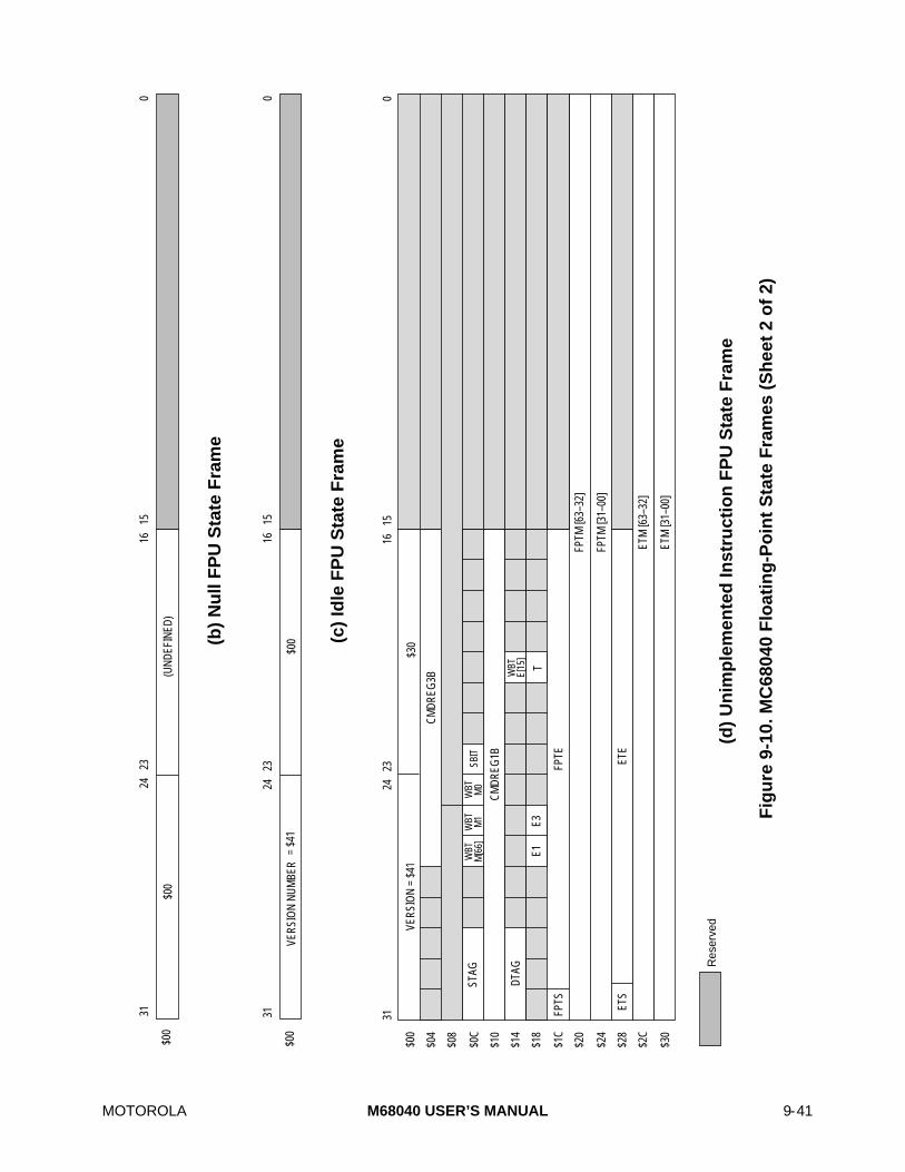
MOTOROLA M68040 USER’S MANUAL 9-41
(d)
Un
imp
lem
ente
d In
stru
ctio
n F
PU
Sta
te F
ram
e
$00
$00
1531
2423
16
(c)
Idle
FP
U S
tate
Fra
me
(b)
Nu
ll F
PU
Sta
te F
ram
e
$00
$00
1531
2423
16
(UND
EFIN
ED)
VERS
ION
NUM
BER
Fig
ure
9-1
0. M
C68
040
Flo
atin
g-P
oin
t S
tate
Fra
mes
(S
hee
t 2
of
2)
Res
erve
d
= $4
1
00
VERS
ION
= $4
1$3
0
STAG
CMDR
EG1B
DTAG
FPTE
FPTM
[63–
32]
E1E3
T
SBIT
CMDR
EG3B
FPTM
[31–
00]
ETE
ETS
ETM
[63–
32]
ETM
[31–
00]
FPTS
E[15
]
M[6
6]M
1M
0
WBT
WBT
WBT
WBT
$04
$08
$18
$20
$24
$28
$1C
$2C
$30
$0C
$10
$14
$00
150
3124
2316

9-42 M68040 USER’S MANUAL MOTOROLA
CMDREG1B—This field contains the command word of the exceptional floating-pointinstruction for an E1 exception, which is an exception detected by the conversion unit(CU) in the floating-point pipeline (see Figure 9-1). For FSQRT, CMDREG1B [6–0] aremapped from $4 for the instruction to $5 in CMDREG1B. All other instructions mapdirectly.
CMDREG3B—This field contains the encoded instruction command word for an E3exception, which is an exception detected by the write-back unit (WB) in the floating-pointpipeline (see Figure 9-1). Figure 9-11 details the bit mapping between CMDREG1B andCMDREG3B. For FSQRT, bits CMDREG1B [6–0] are changed from $4 for the instructionto $5 for CMDREG1B, and therefore map to $21 for CMDREG3B.
CMDREG1B
CMDREG3B
OPCLASS SRC (Rx)
DST (Ry)
CMD
15 13 12 10 9 7 6 0
DST (Ry)
CMD
10 9 7 6 0
0
Figure 9-11. Mapping of Command Bits for CMDREG3B Field
CU_SAVEPC—This field contains the PC for the FPU pipeline’s conversion unit.
E1—If set, this bit indicates that an exception has been detected by the conversion unitpipeline stage. All exception types are possible. The exception handler first checks for anE3 exception and processes it before checking and processing an E1 exception. The E1exception is processed if the E1 bit is set. For the unimplemented instruction state frame,the source operand’s unsupported data type is packed if the E1 bit is set.
E3—If set, this bit indicates that an exception has been detected by the WB pipelinestage. Only OVFL, UNFL, and INEX2 exceptions on opclass 010 or 000 (register toregister and memory to register) for FADD, FSUB, FMUL, FDIV, FSQRT can occur. Theexception handler must check for and process an E3 exception first.
ETS, ETE, ETM—Collectively, these fields are referred to as the ETEMP register andnormally contain the source operand converted to extended precision. If the instructionspecifies a packed decimal real source, bits 63–0 of the operand reside in ETM [63–00],and the ETS and ETE fields are undefined.
FPIARCU—This field contains the instruction address register for the FPU pipeline’sconversion unit.

MOTOROLA M68040 USER’S MANUAL 9-43
FPTS, FPTE, FPTM—Collectively, these fields are referred to as the FPTEMP registerand normally contain the destination operand for dyadic operations converted to extendedprecision. If the instruction specifies a packed decimal real source, bits 95–64 of theoperand reside in FPTM [31–00], and the FPTS, FPTE, and FPTM [63–32] fields areundefined.
OPCLASS—This field refers to bits 15–13 of CMDREG1B. Note that CMDREG1B isidentical to the second word of a floating-point arithmetic instruction opcode.
STAG, DTAG—These 3-bit fields specify the data type of the source and destinationoperands, respectively. STAG is undefined for a packed decimal real source operand. Theencodings for STAG and DTAG are as follows:
000 = Normalized001 = Zero010 = Infinity011 = NAN100 = Extended-Precision Denormalized or Unnormalized Input101 = Single- or Double-Precision Denormalized Input
T—If set, this bit indicates that a post-instruction exception has occurred. Since only anopclass 3 instruction can indicate a post-instruction exception, this bit indicates that theexception is caused by an FMOVE OUT instruction.
WBTS, WBTE [15,14–00], WBTM [66,65–02,01,00], SBIT—These fields contain theexception operand in internal data format for E3 exceptions. Collectively, these fields arecalled the WBTEMP and are an image of the intermediate result. WBTM66 is the overflowbit; WBTM1, WBTM0, and SBIT are the guard, round, and sticky bits, respectively.

9-44 M68040 USER’S MANUAL MOTOROLA
Table 9-16. State Frame Field Information
FSAVE StateFrame Field
Contents
Unimplemented Instruction Exceptions (For Opclass 000 and 010)
CMDREG1B Exception Instruction Command Word
ETEMP Source operand is converted to extended precision. If format is packed, ETM[63–0] contains bits 63–0 of the packed decimal operand.
STAG Source operand tag (undefined if format is packed).
FPTEMP Destination operand, if any, is converted to extended precision. If format ispacked, FPTM [31–0] contains bits 95–64 of the packed decimal operand.
DTAG Destination operand tag, if any.
E1 Always 1
T Always 0
Unsupported Data Type (For Opclass 000 and 010)
CMDREG1B Exception Instruction Command Word
ETEMP Source operand is converted to extended precision. If format is packed, ETM[63–0] contains bits 63–0 of the packed decimal operand.
STAG Source operand tag (undefined if format is packed).
FPTEMP Destination operand, if any, is converted to extended precision. If format ispacked, FPTM [31–0] contains bits 95–64 of the packed decimal operand.
DTAG Destination operand tag, if any.
E1 Always 1
T Always 0
Unsupported Data Type (For Opclass 011)
CMDREG1B FMOVE Command Word
ETEMP Unrounded Source Operand from Floating-Point Data Register
STAG Source Operand Tag
E1 Always 1
T Always 1
SNAN (For Opclass 000 and 010)
CMDREG1B Exception Instruction Command Word
ETEMP Source operand is converted to extended precision.
STAG Source Operand Tag
FPTEMP Destination operand, if any, is converted to extended precision.
DTAG Destination operand tag, if any.
E1 Always 1
T Always 0

MOTOROLA M68040 USER’S MANUAL 9-45
Table 9-16. State Frame Field Information (Continued)
FSAVE StateFrame Field
Contents
SNAN (For Opclass 011)
CMDREG1B FMOVE Instruction Command Word
ETEMP Unrounded Source Operand from Floating-Point Register, with SNAN bit set.
STAG Source Operand Tag, indicated NAN.
E1 Always 1
T Always 1
OPERR (For Opclass 000 and 010)
CMDREG1B Exception Instruction Command Word
ETEMP Source operand is converted to extended precision.
STAG Source Operand Tag
FPTEMP Destination operand, if any, is converted to extended precision.
DTAG Destination operand tag, if any.
E1 Always 1
T Always 0
OPERR (For Opclass 011)
CMDREG1B FMOVE Instruction Command Word
ETEMP Unrounded Source Operand from Floating-Point Register
STAG Source Operand Tag
WBTEMP Contains the rounded integer used to check for erroneous integer overflow.
E1 Always 1
T Always 1
OVFL (FMOVE to Register, FABS, and FNEG)
CMDREG1B Exception Instruction Command Word
FPTEMP Intermediate result with mantissa rounded to correct precision.
STAG Source Operand Tag = Normalized
E1 Always 1
T Always 0
OVFL (FADD, FSUB, FMUL, FDIV, and FSQRT)
CMDREG3B Encoded Exception Instruction Command Word
WBTEMP WBTS, WBTE, and WBTM equal the intermediate result with mantissa roundedto the correct precision.
WBTE15 Bit 15 of the intermediate result's 16-bit exponent = 0 for overflow.
E3 Always 1
T Either 1 or 0

9-46 M68040 USER’S MANUAL MOTOROLA
Table 9-16. State Frame Field Information (Continued)
FSAVE StateFrame Field
Contents
OVFL (FMOVE to Memory)
CMDREG1B FMOVE instruction command word
FPTEMP Intermediate result with mantissa rounded to correct precision.
STAG Source Operand Tag = Normalized
E1 Always 1
T Always 1
UNFL (FMOVE to Register, FABS, and FNEG)
CMDREG1B Exception Instruction Command Word
FPTEMP Unrounded, Extended-Precision Intermediate Result
STAG Source Operand Tag = Normalized
E1 Always 1
T Always 0
UNFL (FADD, FSUB, FMUL, FDIV, and FSQRT)
CMDREG3B Encoded Exception Instruction Command Word
WBTEMP WBTS, WBTE, and WBTM = intermediate result sign, biased 15-bitexponent, and 64-bit mantissa prior to rounding.
WBTE15 Bit 15 of the intermediate result's 16-bit exponent = 1 for underflow.
WBTM1, WBTM0,SBIT
Guard, round, and sticky of intermediate result’s 67-bit mantissa.
E3 Always 1
T Either 1 or 0
UNFL (FMOVE to Memory)
CMDREG1B FMOVE Instruction Command Word
FPTEMP Intermediate result with mantissa prior to rounding.
STAG Source Operand Tag = Normalized
E1 Always 1
T Always 1
DZ
CMDREG1B M68040FPSP divide by zero can generate.
ETEMP Source operand is converted to extended precision.
STAG Source Operand Tag
FPTEMP Destination operand is converted to extended precision.
E1 Always 1
T Always 0
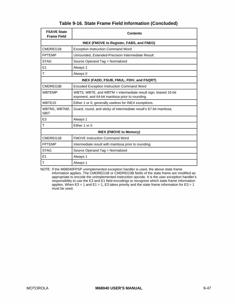
MOTOROLA M68040 USER’S MANUAL 9-47
Table 9-16. State Frame Field Information (Concluded)
FSAVE StateFrame Field
Contents
INEX (FMOVE to Register, FABS, and FNEG)
CMDREG1B Exception Instruction Command Word
FPTEMP Unrounded, Extended-Precision Intermediate Result
STAG Source Operand Tag = Normalized
E1 Always 1
T Always 0
INEX (FADD, FSUB, FMUL, FDIV, and FSQRT)
CMDREG3B Encoded Exception Instruction Command Word
WBTEMP WBTS, WBTE, and WBTM = intermediate result sign, biased 15-bitexponent, and 64-bit mantissa prior to rounding.
WBTE15 Either 1 or 0, generally useless for INEX exceptions.
WBTM1, WBTM0,SBIT
Guard, round, and sticky of intermediate result’s 67-bit mantissa.
E3 Always 1
T Either 1 or 0
INEX (FMOVE to Memory)
CMDREG1B FMOVE Instruction Command Word
FPTEMP Intermediate result with mantissa prior to rounding.
STAG Source Operand Tag = Normalized
E1 Always 1
T Always 1
NOTE: If the M68040FPSP unimplemented exception handler is used, the above state frameinformation applies. The CMDREG1B or CMDREG3B fields of the state frame are modified asappropriate to encode the unimplemented instruction opcode. It is the user exception handler’sresponsibility to use the E3 and E1 field encodings to recognize which state frame informationapplies. When E3 = 1 and E1 = 1, E3 takes priority and the state frame information for E3 = 1must be used.

9-48 M68040 USER’S MANUAL MOTOROLA

MOTOROLA M68040 USER’S MANUAL 10-1
SECTION 10INSTRUCTION TIMINGS
This section summarizes instruction timings for the M68040. The timings are divided intotwo groups: integer unit and floating-point unit instruction timings. Each group is furthersubdivided to separate more complex instruction timings. Each of these subdivided groupsis in alphabetical order with no reference to mode. Table 10-1 alphabetically listsinstruction timings and their location in this section.
Table 10.1. Instruction Timing Index
Instruction Page Instruction Page Instruction Page
ABCD 10-11 BRA 10-11 EOR 10-13
ADD 10-13 BSET 10-15 EORI 10-13
ADDA 10-13 BSR <offset> 10-11 EORI #<xxx>,CCR 10-11
ADDI 10-13 BTST 10-17 EORI #<xxx>,SR 10-11
ADDQ 10-14 CAS 10-17 EXG 10-11
ADDX 10-11 CAS2 10-11 EXT 10-11
AND 10-13 CHK <ea>, Dn 10-17 EXTB 10-11
ANDI 10-13 CHK2 <ea>, Rn 10-18 FABS 10-30,36
ANDI #<xxx>,CCR 10-11 CLR 10-18 FADD 10-30,35
ANDI #<xxx>,SR 10-11 CINV 10-8 FBcc 10-29
ASL 10-14 CMP 10-18 FCMP 10-30,37
ASR 10-14 CMP2 10-19 FDBcc 10-29
Bcc 10-11 CMPA.L 10-19 FDIV 10-30,35
BCHG 10-15 CMPI 10-19 FMOVE 10-30,36
BCLR 10-15 CMPM 10-11 FMOVE FPn,<ea> 10-31
BFCHG 10-15 CPUSH 10-8 FMOVE/FMOVEMto/from CR
10-32
BFCLR 10-15 DBcc 10-11 FMOVEM 10-37
BFEXTS 10-15 DIVS.L 10-20 FMOVEM <ea>,<list> 10-32
BFEXTU 10-15 DIVS.W 10-20 FMOVEM <list>,<ea> 10-32
BFFFO 10-16 DIVSL.L 10-20 FMUL 10-30,35
BFINS 10-16 DIVU.L 10-20 FNEG 10-30,36
BFSET 10-15 DIVU.W 10-20 FNOP 10-29
BFTST 10-16 DIVUL.L 10-20 FRESTORE <ea> 10-34

10-2 M68040 USER’S MANUAL MOTOROLA
Table 10.1. Instruction Timing Index (Continued)
Instruction Page Instruction Page Instruction Page
FSAVE <ea> 10-33 MOVEP 10-11 ROL 10-26
FScc 10-32 MOVEQ 10-11 ROR 10-26
FSQRT 10-30,36 MOVES <ea>,An 10-24 ROXL 10-27
FSUB 10-30,35 MOVES <ea>,Dn 10-24 ROXR 10-27
FTRAPcc 10-29 MOVES Rn,<ea> 10-24 RTD 10-11
FTST <ea>, FPn 10-30 MULS.W/L 10-25 RTE 10-11
ILLEGAL 10-11 MULU.W/L 10-25 RTR 10-11
JMP 10-20 NBCD 10-25 RTS 10-11
JSR 10-21 NEG 10-26 SBCD 10-11
LEA 10-21 NEGX 10-26 Scc 10-27
LINK 10-11 NOP 10-11 SUB 10-13
LSL 10-14 NOT 10-26 SUBA 10-27
LSR 10-14 OR 10-13 SUBI 10-13
MOVE 10-9,10 ORI 10-13 SUBQ 10-14
MOVE from CCR 10-21 ORI #<xxx>,CCR 10-11 SUBX 10-11
MOVE from SR 10-22 ORI #<xxx>,SR 10-11 SWAP 10-11
MOVE to CCR 10-22 PACK 10-11 TAS 10-28
MOVE to SR 10-22 PEA 10-26 TRAP# 10-11
MOVE USP 10-11 PFLUSH 10-11 TRAPcc 10-11
MOVE16 10-11 PFLUSHA 10-11 TRAPV 10-11
MOVEA.L 10-23 PFLUSHAN 10-11 TST 10-13
MOVEC 10-11 PFLUSHN (An) 10-11 UNLK 10-11
MOVEM <list>,<ea> 10-23 PTESTR, PTESTW 10-11 UNPK 10-11
MOVEM.L <ea>,<list> 10-23 RESET 10-11
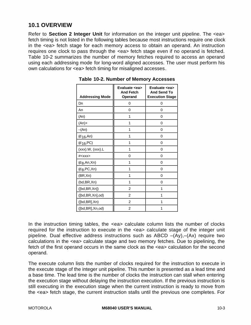
MOTOROLA M68040 USER’S MANUAL 10-3
10.1 OVERVIEW
Refer to Section 2 Integer Unit for information on the integer unit pipeline. The <ea>fetch timing is not listed in the following tables because most instructions require one clockin the <ea> fetch stage for each memory access to obtain an operand. An instructionrequires one clock to pass through the <ea> fetch stage even if no operand is fetched.Table 10-2 summarizes the number of memory fetches required to access an operandusing each addressing mode for long-word aligned accesses. The user must perform hisown calculations for <ea> fetch timing for misaligned accesses.
Table 10-2. Number of Memory Accesses
Addressing Mode
Evaluate <ea>And FetchOperand
Evaluate <ea>And Send To
Execution Stage
Dn 0 0
An 0 0
(An) 1 0
(An)+ 1 0
–(An) 1 0
(d16,An) 1 0
(d16,PC) 1 0
(xxx).W, (xxx).L 1 0
#<xxx> 0 0
(d8,An,Xn) 1 0
(d8,PC,Xn) 1 0
(BR,Xn) 1 0
(bd,BR,Xn) 1 0
([bd,BR,Xn]) 2 1
([bd,BR,Xn],od) 2 1
([bd,BR],Xn) 2 1
([bd,BR],Xn,od) 2 1
In the instruction timing tables, the <ea> calculate column lists the number of clocksrequired for the instruction to execute in the <ea> calculate stage of the integer unitpipeline. Dual effective address instructions such as ABCD –(Ay),–(Ax) require twocalculations in the <ea> calculate stage and two memory fetches. Due to pipelining, thefetch of the first operand occurs in the same clock as the <ea> calculation for the secondoperand.
The execute column lists the number of clocks required for the instruction to execute inthe execute stage of the integer unit pipeline. This number is presented as a lead time anda base time. The lead time is the number of clocks the instruction can stall when enteringthe execution stage without delaying the instruction execution. If the previous instruction isstill executing in the execution stage when the current instruction is ready to move fromthe <ea> fetch stage, the current instruction stalls until the previous one completes. For
10-4 M68040 USER’S MANUAL MOTOROLA
example, if an execution time is listed as 2L + 1, the lead time is two clocks and the basetime is one for a total execution time of three. The instruction can stall for two clockswithout delaying the instruction execution time.
The <ea> calculate and execute stages operate in an interlocked manner for allinstructions using the brief and full extension word formats. If an instruction using one ofthese formats is stalled for more than NL clocks waiting to begin execution in the executestage, a similar increase in the <ea> calculate time will result. For example, if theexecution time listed is 2L + 1 and the instruction stalls for three clocks, then the <ea>calculate time increases by one clock (3 – 1 = 2L). Write-back times are not listed becausethey are system dependent and do not affect either <ea> calculate or execute stages ofthe pipeline.
Not all addressing modes listed in the following tables for an instruction are valid for allvariations of the instruction. For example, the table for the integer ADD instruction liststimes for both ADD <ea>,Dn and ADD Dn,<ea>. All addressing modes listed are valid forADD <ea>,Dn. For ADD Dn,<ea> the following invalid modes should be ignored: An,(d16,PC), #<xxx>, (d8,PC,Xn), and modes with BR = PC. Refer to the M68000PM/AD,M68000 Family Programmer's Reference Manual for a complete summary of validinstruction and addressing mode combinations. The instruction timings are based on thefollowing suppositions unless otherwise noted:
1. All timings are related to BCLK cycles and are for BR = An or suppressed. For BR =PC, 1 and 1L clocks to the <ea> calculate and execution times unless otherwisenoted. For memory indirect postindexed with suppressed index — ([bd,BR],Xn) or([bd,BR],Xn,od) with Xn suppressed — times are the same as for memory indirectpreindexed with suppressed index — ([bd,BR,Xn]) or ([bd,BR,Xn],od) with Xnsuppressed.
2. All memory accesses hit in the caches; no table searches occur as a result of ATCmisses except for the operand accesses for the CAS, CAS2, and TAS instructions.These accesses are implicitly noncachable and force external bus accesses. It isassumed that external memory has a zero-wait state in this case and that the bus isgranted to the M68040.
The result increases access time equal to the number of clocks for the memoryaccess (first bus cycle if the operand access results in a line memory access) ifaligned accesses miss in the data cache. As an approximation, this time should beadded to the execution time for each operand fetch generated by the instruction.
3. All accesses are aligned to a byte boundary that is a multiple of the operand size.For instance, the timing for all long-word accesses assumes that the operands areon long-word boundaries.
4. The integer execution times for floating-point instructions assume that the floating-point unit (FPU) is idle.
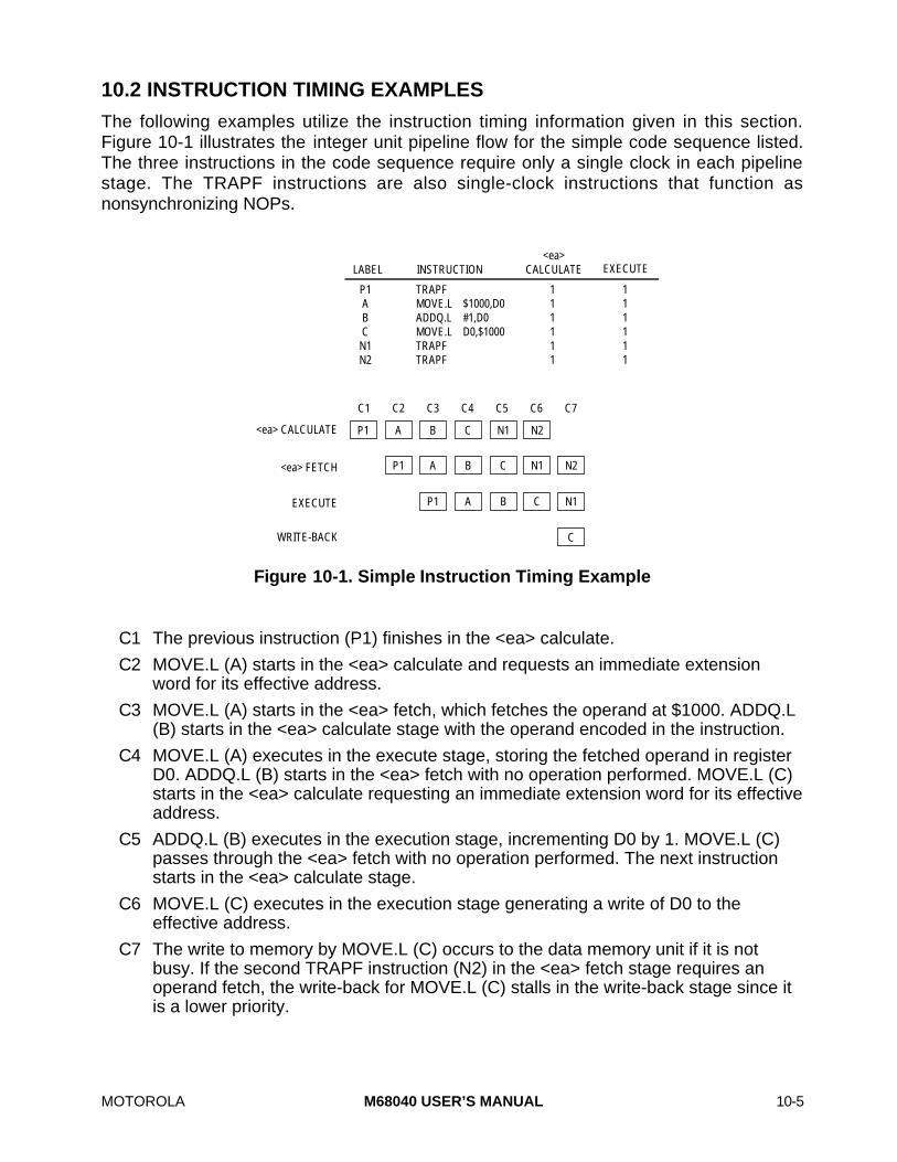
MOTOROLA M68040 USER’S MANUAL 10-5
10.2 INSTRUCTION TIMING EXAMPLES
The following examples utilize the instruction timing information given in this section.Figure 10-1 illustrates the integer unit pipeline flow for the simple code sequence listed.The three instructions in the code sequence require only a single clock in each pipelinestage. The TRAPF instructions are also single-clock instructions that function asnonsynchronizing NOPs.
LABEL
P1 A B C
N1 N2
INSTRUCTION
TRAPF MOVE.L ADDQ.L MOVE.L TRAPF TRAPF
<ea> CALCULATE
1 1 1 1 1 1
EXECUTE
$1000,D0 #1,D0 D0,$1000
1 1 1 1 1 1
C1 C2 C3 C4 C5 C6 C7
P1 A B C N1 N2
P1 A B C N1 N2
P1 A B C N1
<ea> CALCULATE
<ea> FETCH
EXECUTE
WRITE-BACK C
Figure 10-1. Simple Instruction Timing Example
C1 The previous instruction (P1) finishes in the <ea> calculate.
C2 MOVE.L (A) starts in the <ea> calculate and requests an immediate extensionword for its effective address.
C3 MOVE.L (A) starts in the <ea> fetch, which fetches the operand at $1000. ADDQ.L(B) starts in the <ea> calculate stage with the operand encoded in the instruction.
C4 MOVE.L (A) executes in the execute stage, storing the fetched operand in registerD0. ADDQ.L (B) starts in the <ea> fetch with no operation performed. MOVE.L (C)starts in the <ea> calculate requesting an immediate extension word for its effectiveaddress.
C5 ADDQ.L (B) executes in the execution stage, incrementing D0 by 1. MOVE.L (C)passes through the <ea> fetch with no operation performed. The next instructionstarts in the <ea> calculate stage.
C6 MOVE.L (C) executes in the execution stage generating a write of D0 to theeffective address.
C7 The write to memory by MOVE.L (C) occurs to the data memory unit if it is notbusy. If the second TRAPF instruction (N2) in the <ea> fetch stage requires anoperand fetch, the write-back for MOVE.L (C) stalls in the write-back stage since itis a lower priority.

10-6 M68040 USER’S MANUAL MOTOROLA
The separation of calculation and execution in the <ea> calculate and execute stagesallows instruction reordering during compile time to take advantage of potential instructionoverlap. Figure 10-2 illustrates this overlap for an instruction requiring multiple clocks inthe execute stage and with an instruction with a long lead time. The execution time forLEA (3L + 1) indicates that the instruction can be stalled three clocks without affectingexecution.
When the LEA (A) instruction precedes the ABCD (B) instruction, the execution stallsduring C4–C6 (equivalent to the LEA lead time) while the instruction completes in the<ea> calculate and <ea> fetch stages. The resulting execution time for the LEA (A) andABCD (B) sequence is eight clocks.
However, if the LEA (C) instruction follows the ABCD (B) instruction, the LEA stalls in the<ea> fetch instead, during C9–C11. The LEA then executes in a single clock in theexecution stage. The resulting execution time for the LEA (C) and ABCD (B) sequence isfive clocks.
LABEL P1
A B C
N1 N2
INSTRUCTION TRAPF LEA ABCD LEA TRAPF TRAPF
<ea> CALCULATE
1 4 1 4 1 1
EXECUTE
$24(PC),A1 D0,D1 $24(PC),A1
1 3L + 1
3 3L + 1
1 1
C1 C2 C3 C4 C5 C6 C7 C8 C9 C10 C11 C12 C13
P1 A A A A B C C C C N1 N2<ea> CALCULATE
<ea> FETCH
EXECUTE
WRITE-BACK
P1 A A A A B C CL1 CL2 CL3 N1 N2
P1 AL AL AL A B B B C* C N1
NOTE: *Possible stalls in this stage.
Figure 10-2. Instruction Overlap with Multiple Clocks

MOTOROLA M68040 USER’S MANUAL 10-7
Instructions using the brief and full extension word format addressing modes cause the<ea> calculate and execute stages to operate in an interlocked manner. When theseinstructions wait to begin execution in the execution stage, there is a similar increase inthe <ea> calculate time. Figure 10-3 illustrates this effect for an ADD instruction using abrief format extension word. The ADD instruction stalls for two clocks waiting to enter theexecution stage. Since this time exceeds by one clock the ADD lead time, the ADDinstruction remains in the <ea> calculate stage for one additional clock. If the ADDinstruction was in the execution stage for two clocks, the ABCD instruction would not havestalled in the <ea> calculate stage.
LABEL P1
A B
N1 N2
INSTRUCTION TRAPF ABCD ADD.L TRAPF TRAPF
<ea> CALCULATE
1 3 5 1 1
EXECUTE
D0,D1 4(A0,D3),D2
1 3
1L + 4 1 1
C1 C2 C3 C4 C5 C6 C7 C8 C9 C10 C11 C12
P1 A B B B B* B B N1 N2<ea> CALCULATE
<ea> FETCH
EXECUTE
WRITE-BACK
P1 A
P1 A
B B B B B B N1 N2
A A B B B B N1 N2
NOTE: *Possible stalls in this stage.
Figure 10-3. Interlocked Stages
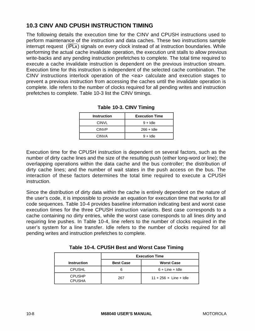
10-8 M68040 USER’S MANUAL MOTOROLA
10.3 CINV AND CPUSH INSTRUCTION TIMING
The following details the execution time for the CINV and CPUSH instructions used toperform maintenance of the instruction and data caches. These two instructions sampleinterrupt request (IPL≈) signals on every clock instead of at instruction boundaries. Whileperforming the actual cache invalidate operation, the execution unit stalls to allow previouswrite-backs and any pending instruction prefetches to complete. The total time required toexecute a cache invalidate instruction is dependent on the previous instruction stream.Execution time for this instruction is independent of the selected cache combination. TheCINV instructions interlock operation of the <ea> calculate and execution stages toprevent a previous instruction from accessing the caches until the invalidate operation iscomplete. Idle refers to the number of clocks required for all pending writes and instructionprefetches to complete. Table 10-3 list the CINV timings.
Table 10-3. CINV Timing
Instruction Execution Time
CINVL 9 + Idle
CINVP 266 + Idle
CINVA 9 + Idle
Execution time for the CPUSH instruction is dependent on several factors, such as thenumber of dirty cache lines and the size of the resulting push (either long-word or line); theoverlapping operations within the data cache and the bus controller; the distribution ofdirty cache lines; and the number of wait states in the push access on the bus. Theinteraction of these factors determines the total time required to execute a CPUSHinstruction.
Since the distribution of dirty data within the cache is entirely dependent on the nature ofthe user’s code, it is impossible to provide an equation for execution time that works for allcode sequences. Table 10-4 provides baseline information indicating best and worst caseexecution times for the three CPUSH instruction variants. Best case corresponds to acache containing no dirty entries, while the worst case corresponds to all lines dirty andrequiring line pushes. In Table 10-4, line refers to the number of clocks required in theuser’s system for a line transfer. Idle refers to the number of clocks required for allpending writes and instruction prefetches to complete.
Table 10-4. CPUSH Best and Worst Case Timing
Execution Time
Instruction Best Case Worst Case
CPUSHL 6 6 + Line + Idle
CPUSHPCPUSHA
267 11 + 256 × Line + Idle

MOTOROLA M68040 USER’S MANUAL 10-9
10.4 MOVE INSTRUCTION TIMING
DESTINATION
Dn (An) (An)+
SOURCE<ea>
CalculateExecute <ea>
CalculateExecute <ea>
CalculateExecute
Dn 1 1 1 1 1 1
(An) 1 1 1 1 2 1L + 1
(An)+ 1 1 2 1L + 1 2 1L + 1
–(An) 1 1 2 1L + 1 2 1L + 1
(d16,An) 1 1 2 1L + 1 2 1L + 1
(d16,PC) 3 2L + 1 3 2L + 1 3 2L + 1
(xxx).W, (xxx).L 1 1 1 1 2 1L + 1
#<xxx> 1 1 1 1 2 1L + 1
(d8,An,Xn) 3 3 4 4 5 5
(d8,PC,Xn) 5 1L + 4 5 1L + 4 6 1L + 5
(b16,BR,Xn) 7 1L + 6 7 1L + 6 8 1L + 7
([bd,BR,Xn]) 10 1L + 9 10 1L + 9 11 1L + 10
([bd,BR,Xn],od) 11 1L + 10 11 1L + 10 12 1L + 11
([bd,BR],Xn) 11 3L + 8 11 3L + 8 12 3L + 9
([bd,BR],Xn,od) 12 3L + 9 12 3L + 9 13 3L + 10
–(An) (d16,An) (xxx).W, (xxx).L
Dn 1 1 1 1 1 1
(An) 2 1L + 1 2 1L + 1 1 1
(An)+ 2 1L + 1 2 1L + 1 2 1L + 1
–(An) 2 1L + 1 2 1L + 1 2 1L + 1
(d16,An) 2 1L + 1 2 1L + 1 2 1L + 1
(d16,PC) 3 2L + 1 4 3L + 1 4 3L + 1
(xxx).W, (xxx).L 2 1L + 1 2 1L + 1 2 1L + 1
#<xxx> 2 1L + 1 2 1L + 1 2 1L + 1
(d8,An,Xn) 5 5 5 5 5 5
(d8,PC,Xn) 6 1L + 5 6 1L + 5 6 1L + 5
(b16,BR,Xn) 8 1L + 7 8 1L + 7 8 1L + 7
([bd,BR,Xn]) 11 1L + 10 11 1L + 10 11 1L + 10
([bd,BR,Xn],od) 12 1L + 11 12 1L + 11 12 1L + 11
([bd,BR],Xn) 12 3L + 9 12 3L + 9 12 3L + 9
([bd,BR],Xn,od) 13 3L + 10 13 3L + 10 13 3L + 10
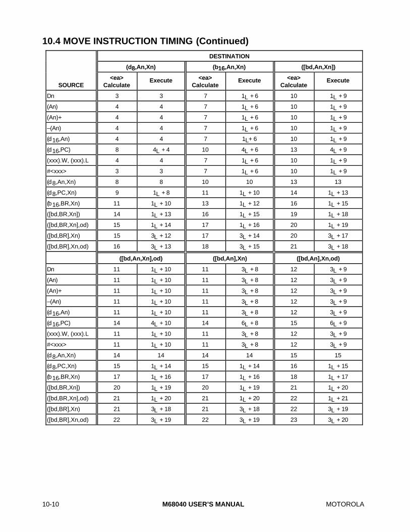
10-10 M68040 USER’S MANUAL MOTOROLA
10.4 MOVE INSTRUCTION TIMING (Continued)
DESTINATION
(d8,An,Xn) (b16,An,Xn) ([bd,An,Xn])
SOURCE<ea>
CalculateExecute <ea>
CalculateExecute <ea>
CalculateExecute
Dn 3 3 7 1L + 6 10 1L + 9
(An) 4 4 7 1L + 6 10 1L + 9
(An)+ 4 4 7 1L + 6 10 1L + 9
–(An) 4 4 7 1L + 6 10 1L + 9
(d16,An) 4 4 7 1L+ 6 10 1L + 9
(d16,PC) 8 4L + 4 10 4L + 6 13 4L + 9
(xxx).W, (xxx).L 4 4 7 1L + 6 10 1L + 9
#<xxx> 3 3 7 1L + 6 10 1L + 9
(d8,An,Xn) 8 8 10 10 13 13
(d8,PC,Xn) 9 1L + 8 11 1L + 10 14 1L + 13
(b16,BR,Xn) 11 1L + 10 13 1L + 12 16 1L + 15
([bd,BR,Xn]) 14 1L + 13 16 1L + 15 19 1L + 18
([bd,BR,Xn],od) 15 1L + 14 17 1L + 16 20 1L + 19
([bd,BR],Xn) 15 3L + 12 17 3L + 14 20 3L + 17
([bd,BR],Xn,od) 16 3L + 13 18 3L + 15 21 3L + 18
([bd,An,Xn],od) ([bd,An],Xn) ([bd,An],Xn,od)
Dn 11 1L + 10 11 3L + 8 12 3L + 9
(An) 11 1L + 10 11 3L + 8 12 3L + 9
(An)+ 11 1L + 10 11 3L + 8 12 3L + 9
–(An) 11 1L + 10 11 3L + 8 12 3L + 9
(d16,An) 11 1L + 10 11 3L + 8 12 3L + 9
(d16,PC) 14 4L + 10 14 6L + 8 15 6L + 9
(xxx).W, (xxx).L 11 1L + 10 11 3L + 8 12 3L + 9
#<xxx> 11 1L + 10 11 3L + 8 12 3L + 9
(d8,An,Xn) 14 14 14 14 15 15
(d8,PC,Xn) 15 1L + 14 15 1L + 14 16 1L + 15
(b16,BR,Xn) 17 1L + 16 17 1L + 16 18 1L + 17
([bd,BR,Xn]) 20 1L + 19 20 1L + 19 21 1L + 20
([bd,BR,Xn],od) 21 1L + 20 21 1L + 20 22 1L + 21
([bd,BR],Xn) 21 3L + 18 21 3L + 18 22 3L + 19
([bd,BR],Xn,od) 22 3L + 19 22 3L + 19 23 3L + 20
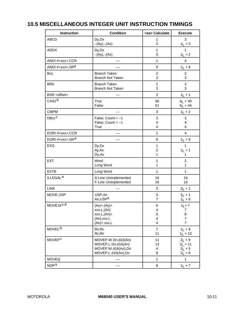
MOTOROLA M68040 USER’S MANUAL 10-11
10.5 MISCELLANEOUS INTEGER UNIT INSTRUCTION TIMINGS
Instruction Condition <ea> Calculate Execute
ABCD Dy,Dx–(Ay),–(Ax)
13
31L + 3
ADDX Dy,Dx–(Ay),–(Ax)
13
11L + 2
ANDI #<xxx>,CCR — 1 4
ANDI #<xxx>,SRa — 9 1L + 8
Bcc Branch TakenBranch Not Taken
23
23
BRA Branch TakenBranch Not Taken
23
23
BSR <offset> — 2 1L + 1
CAS2b TrueFalse
5651
6L + 496L + 44
CMPM — 3 1L + 2
DBccc False, Count > –1False, Count = –1True
344
344
EORI #<xxx>,CCR — 1 4
EORI #<xxx>,SRa — 9 1L + 8
EXG Dy,DxAy,AxDy,Ax
121
11L + 1
1
EXT WordLong Word
11
21
EXTB Long Word 1 1
ILLEGALa A-Line UnimplementedF-Line Unimplemented
1616
1616
LINK — 3 2L + 1
MOVE USP USP,AnAn,USPa
37
2L + 11L + 6
MOVE16c,d (Ax)+,(Ay)+xxx.L,(An)xxx.L,(An)+(An),xxx.L(An)+,xxx.L
64544
1L+ 77877
MOVECb Rn,RcRc,Rn
711
1L + 61L + 10
MOVEPc MOVEP.W Dn,d16(An)MOVEP.L Dn,d16(An)MOVEP.W d16(An),DnMOVEP.L d16(An),Dn
111348
2L + 92L + 112L + 52L + 8
MOVEQ — 1 1
NOPa — 8 1L + 7

10-12 M68040 USER’S MANUAL MOTOROLA
10.5 MISCELLANEOUS INTEGER UNIT INSTRUCTION TIMINGS (Continued)
Instruction Condition <ea> Calculate Execute
ORI #<xxx>,CCR — 1 4
ORI #<xxx>,SRa — 9 1L + 8
PACK Dx,Dy,#<xxx>–(Ay),–(Ax),#<xxx>
13
32L + 3
PFLUSHb — 11 1L + 10
PFLUSHAb — 11 1L + 10
PFLUSHANb — 27 1L + 26
PFLUSHN (An)b — 11 1L + 10
PTESTR, PTESTWe — 25 11L + 14
RESETa — 521 521
RTDc — 6 1L + 5
RTEa Stack Format $0Stack Format $1Stack Format $2Stack Format $3Stack Format $4Stack Format $7
242324
132314201523
RTRc — 7 1L + 6
RTSc — 5 5
SBCD Dy,Dx–(Ay),–(Ax)
13
31L + 3
SUBX Dy,Dx–(Ay),–(Ax)
13
11L + 2
SWAP — 1 2
TRAP#a — 16 16
TRAPccf TakenNot Taken
195
195
TRAPVf TakenNot Taken
195
195
UNLK — 2 1L + 1
UNPK Dx,Dy,#–(Ay),–(Ax),#
13
42L + 4
NOTES:a. Times listed are minimum. This instruction interlocks the <ea> calculate and execute
stages and synchronizes some portions of the processor before execution.b. Times listed are typical. This instruction interlocks the <ea> calculate and execute stages
and synchronizes some portions of the processor before execution.c. This instruction interlocks the <ea> calculate and execute stages.d. Successive in-line MOVE16 instructions each add eight clocks to the <ea> calculate and
execute times.e. Typical measurement for three-level table search with no descriptor writes, no entries
cached, and four-clock memory access times.f. This instruction interlocks the <ea> calculate and execute stages. For the exception taken,
this instruction also synchronizes some portions of the processor before execution; timeslisted are minimum in this case.
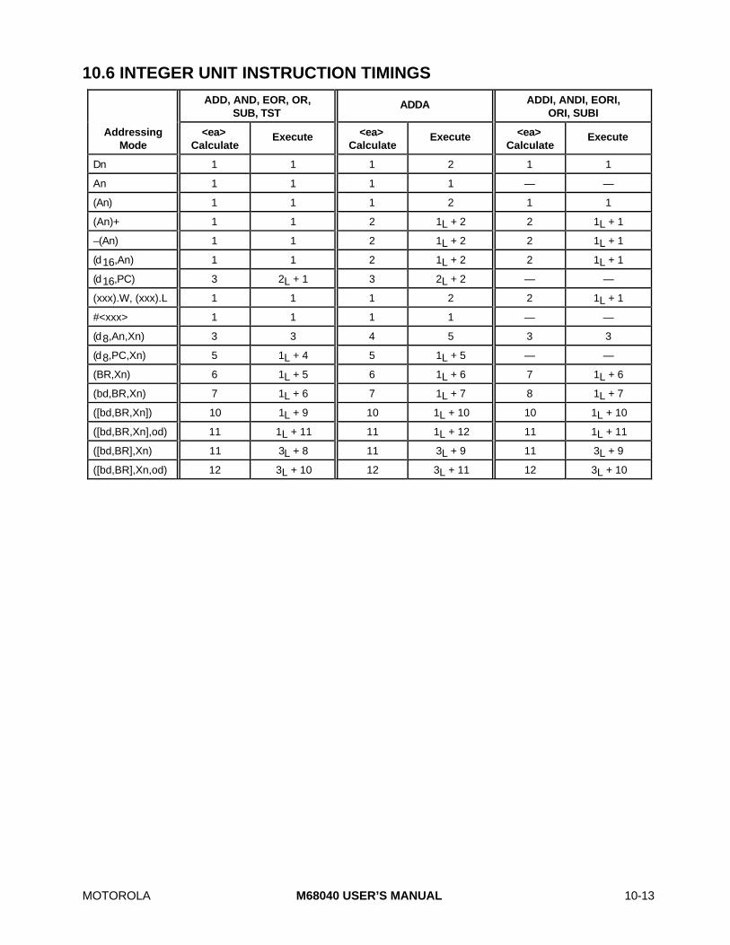
MOTOROLA M68040 USER’S MANUAL 10-13
10.6 INTEGER UNIT INSTRUCTION TIMINGS
ADD, AND, EOR, OR,SUB, TST
ADDA ADDI, ANDI, EORI,ORI, SUBI
AddressingMode
<ea>Calculate
Execute <ea>Calculate
Execute <ea>Calculate
Execute
Dn 1 1 1 2 1 1
An 1 1 1 1 — —
(An) 1 1 1 2 1 1
(An)+ 1 1 2 1L + 2 2 1L + 1
–(An) 1 1 2 1L + 2 2 1L + 1
(d16,An) 1 1 2 1L + 2 2 1L + 1
(d16,PC) 3 2L + 1 3 2L + 2 — —
(xxx).W, (xxx).L 1 1 1 2 2 1L + 1
#<xxx> 1 1 1 1 — —
(d8,An,Xn) 3 3 4 5 3 3
(d8,PC,Xn) 5 1L + 4 5 1L + 5 — —
(BR,Xn) 6 1L + 5 6 1L + 6 7 1L + 6
(bd,BR,Xn) 7 1L + 6 7 1L + 7 8 1L + 7
([bd,BR,Xn]) 10 1L + 9 10 1L + 10 10 1L + 10
([bd,BR,Xn],od) 11 1L + 11 11 1L + 12 11 1L + 11
([bd,BR],Xn) 11 3L + 8 11 3L + 9 11 3L + 9
([bd,BR],Xn,od) 12 3L + 10 12 3L + 11 12 3L + 10

10-14 M68040 USER’S MANUAL MOTOROLA
10.6 INTEGER UNIT INSTRUCTION TIMINGS (Continued)
ADDQ, SUBQ ASL ASR, LSL, LSR
AddressingMode
<ea>Calculate
Execute <ea>Calculate
Execute <ea>Calculate
Execute
Dn 1 1 1 3/4* 1 2/3*
An 1 1 — — — —
(An) 1 1 1 3 1 2
(An)+ 2 1L + 1 1 3 1 2
–(An) 2 1L + 1 1 3 1 2
(d16,An) 2 1L + 1 1 3 1 2
(d16,PC) — — — — — —
(xxx).W, (xxx).L 1 1 1 3 1 2
#<xxx> — — — — — —
(d8,An,Xn) 3 3 3 5 3 4
(d8,PC,Xn) — — — — — —
(BR,Xn) 7 1L + 6 7 1L + 8 7 1L + 7
(bd,BR,Xn) 8 1L + 7 8 1L + 9 8 1L + 8
([bd,BR,Xn]) 10 1L + 9 10 1L + 11 10 1L + 10
([bd,BR,Xn],od) 11 1L + 11 11 1L + 12 11 1L + 11
([bd,BR],Xn) 11 3L + 8 11 3L + 10 11 3L + 9
([bd,BR],Xn,od) 12 3L + 10 12 3L + 11 12 3L + 10
*Immediate count specified for shift count/shift count specified in register, respectively.

MOTOROLA M68040 USER’S MANUAL 10-15
10.6 INTEGER UNIT INSTRUCTION TIMINGS (Continued)
BCHG, BCLR, BSETa BFCHG, BFCLR, BFSETb,c BFEXTS, BFEXTUb,d
AddressingMode
<ea>Calculate
Execute <ea>Calculate
Execute <ea>Calculate
Execute
Dn 1 3/4 3/4e 6/7e 1/2e 4/5e
An — — — — — —
(An) 1 3/4 9 2L + 8 9 2L + 7
(An)+ 1 3/4 — — — —
–(An) 1 3/4 — — — —
(d16,An) 2/1 1L + 3/4 9 2L + 8 9 2L + 7
(d16,PC) — — — — 10 3L + 7
(xxx).W, (xxx).L 2/1 1L + 3/4 9 2L + 8 9 2L + 7
#<xxx> — — — — — —
(d8,An,Xn) 3 5/6 10 11 10 10
(d8,PC,Xn) — — — — 11 1L + 10
(BR,Xn) 7 1L + 8/1L + 9 13 1L + 13 13 1L + 12
(bd,BR,Xn) 8 1L + 9/1L + 10 14 1L + 14 14 1L + 13
([bd,BR,Xn]) 10 1L + 11/1L + 12 16 1L + 16 16 1L + 15
([bd,BR,Xn],od) 11 1L + 12/1L + 13 17 1L + 17 17 1L + 16
([bd,BR],Xn) 11 3L + 10/3L + 11 17 3L + 15 17 3L + 14
([bd,BR],Xn,od) 12 3L + 11/3L + 12 18 3L + 16 18 3L + 15
NOTES:a. Bit instruction <ea> calculate and execute times T1/T2 apply to #<xxx>/Dn bit numbers.b. This instruction interlocks the <ea> calculate and execute stages.c. If the bit field spans a long-word boundary, add ten and nine clocks to the <ea> calculate and execute times,
respectively. Two memory addresses are accessed in this case.d. If the bit field spans a long-word boundary, add two clocks to the execute time. Two memory addresses are
accessed in this case.e. Immediate count specified for both width and offset and width and/or offset specified in register, respectively.
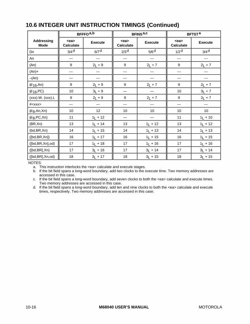
10-16 M68040 USER’S MANUAL MOTOROLA
10.6 INTEGER UNIT INSTRUCTION TIMINGS (Continued)
BFFFOa,b BFINSa,c BFTSTa
AddressingMode
<ea>Calculate
Execute <ea>Calculate
Execute <ea>Calculate
Execute
Dn 3/4d 6/7d 2/3d 5/6d 1/2d 3/4d
An — — — — — —
(An) 9 2L + 9 9 2L + 7 9 2L + 7
(An)+ — — — — — —
–(An) — — — — — —
(d16,An) 9 2L + 9 9 2L + 7 9 2L + 7
(d16,PC) 10 3L + 9 — — 10 3L + 7
(xxx).W, (xxx).L 9 2L + 9 9 2L + 7 9 2L + 7
#<xxx> — — — — — —
(d8,An,Xn) 10 12 10 10 10 10
(d8,PC,Xn) 11 1L + 12 — — 11 1L + 10
(BR,Xn) 13 1L + 14 13 1L + 12 13 1L + 12
(bd,BR,Xn) 14 1L + 15 14 1L + 13 14 1L + 13
([bd,BR,Xn]) 16 1L + 17 16 1L + 15 16 1L + 15
([bd,BR,Xn],od) 17 1L + 18 17 1L + 16 17 1L + 16
([bd,BR],Xn) 17 3L + 16 17 3L + 14 17 3L + 14
([bd,BR],Xn,od) 18 3L + 17 18 3L + 15 18 3L + 15
NOTES:a. This instruction interlocks the <ea> calculate and execute stages.b. If the bit field spans a long-word boundary, add two clocks to the execute time. Two memory addresses are
accessed in this case.c. If the bit field spans a long-word boundary, add seven clocks to both the <ea> calculate and execute times.
Two memory addresses are accessed in this case.d. If the bit field spans a long-word boundary, add ten and nine clocks to both the <ea> calculate and execute
times, respectively. Two memory addresses are accessed in this case.

MOTOROLA M68040 USER’S MANUAL 10-17
10.6 INTEGER UNIT INSTRUCTION TIMINGS (Continued)
BTST CASb CHKc,d (<ea>, Dn)
AddressingMode
<ea>Calculate
Execute <ea>Calculate
Execute <ea>Calculate
Execute
Dn 1 1/2a — — 8 1L + 7
An — — — — — —
(An) 1 1/2 36 6L + 31 9 2L + 7
(An)+ 1 1/2 37 5L + 31 9 2L + 7
–(An) 1 1/2 37 5L + 31 9 2L + 7
(d16,An) 2/1 1L + 1/2 37 5L + 31 9 2L + 7
(d16,PC) 3 2L + 1/2L + 2 — — 10 3L + 7
(xxx).W, (xxx).L 2/1 1L + 1/2 36 5L + 31 9 2L + 7
#<xxx> — — — — 8 1L + 7
(d8,An,Xn) 3 3/4 36 36 10 10
(d8,PC,Xn) 5 1L + 4/1L + 5 — — 11 1L + 10
(BR,Xn) 7/6 1L + 6/1L + 7 36 1L + 35 12 1L + 11
(bd,BR,Xn) 8/7 1L + 7/1L + 8 37 1L + 36 13 1L + 12
([bd,BR,Xn]) 10/9 1L + 9/1L + 10 42 40 16 1L + 15
([bd,BR,Xn],od) 11/10 1L + 10/1L + 11 42 1L + 41 17 1L + 16
([bd,BR],Xn) 11/10 3L + 8/3L + 9 42 3L + 38 17 3L + 14
([bd,BR],Xn,od) 12/11 3L + 9/3L + 10 42 3L + 39 18 3L + 15
NOTES:a. Bit instruction <ea> calculate and execute times T1/T2 apply to #<xxx>/Dn bit numbers.b. Times listed are typical. This instruction interlocks the <ea> calculate and execute stages and synchronizes
some portions of the processor before execution.c. This instruction interlocks the <ea> calculate and execute stages.d. Times listed are for Dn within bounds. This instruction interlocks the <ea> calculate and execute stages.
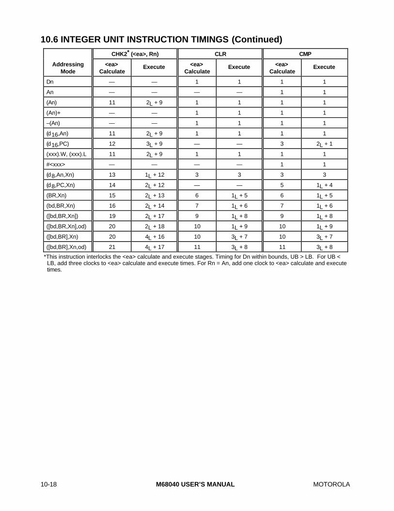
10-18 M68040 USER’S MANUAL MOTOROLA
10.6 INTEGER UNIT INSTRUCTION TIMINGS (Continued)
CHK2* (<ea>, Rn) CLR CMP
AddressingMode
<ea>Calculate
Execute <ea>Calculate
Execute <ea>Calculate
Execute
Dn — — 1 1 1 1
An — — — — 1 1
(An) 11 2L + 9 1 1 1 1
(An)+ — — 1 1 1 1
–(An) — — 1 1 1 1
(d16,An) 11 2L + 9 1 1 1 1
(d16,PC) 12 3L + 9 — — 3 2L + 1
(xxx).W, (xxx).L 11 2L + 9 1 1 1 1
#<xxx> — — — — 1 1
(d8,An,Xn) 13 1L + 12 3 3 3 3
(d8,PC,Xn) 14 2L + 12 — — 5 1L + 4
(BR,Xn) 15 2L + 13 6 1L + 5 6 1L + 5
(bd,BR,Xn) 16 2L + 14 7 1L + 6 7 1L + 6
([bd,BR,Xn]) 19 2L + 17 9 1L + 8 9 1L + 8
([bd,BR,Xn],od) 20 2L + 18 10 1L + 9 10 1L + 9
([bd,BR],Xn) 20 4L + 16 10 3L + 7 10 3L + 7
([bd,BR],Xn,od) 21 4L + 17 11 3L + 8 11 3L + 8
*This instruction interlocks the <ea> calculate and execute stages. Timing for Dn within bounds, UB > LB. For UB <LB, add three clocks to <ea> calculate and execute times. For Rn = An, add one clock to <ea> calculate and executetimes.

MOTOROLA M68040 USER’S MANUAL 10-19
10.6 INTEGER UNIT INSTRUCTION TIMINGS (Continued)
CMPA.L CMPI CMP2*
AddressingMode
<ea>Calculate
Execute <ea>Calculate
Execute <ea>Calculate
Execute
Dn 1 1 1 1 — —
An 1 1 — — — —
(An) 1 1 1 1 13 2L + 11
(An)+ 2 1L + 1 2 1L + 1 0 0
–(An) 2 1L + 1 2 1L + 1 0 0
(d16,An) 2 1L + 1 2 1L + 1 13 2L + 11
(d16,PC) 3 2L + 1 3 2L + 1 14 3L + 11
(xxx).W, (xxx).L 1 1 2 1L + 1 13 2L + 11
#<xxx> 1 1 — — — —
(d8,An,Xn) 3 3 3 3 15 1L + 14
(d8,PC,Xn) 5 1L + 4 5 2L + 4 16 2L + 14
(BR,Xn) 6 1L + 5 6 2L + 5 17 2L + 15
(bd,BR,Xn) 7 1L + 6 7 2L + 6 18 2L + 16
([bd,BR,Xn]) 9 1L + 8 9 2L + 8 21 2L + 19
([bd,BR,Xn],od) 10 1L + 9 10 2L + 9 22 2L + 20
([bd,BR],Xn) 10 3L + 7 10 4L + 7 22 4L + 18
([bd,BR],Xn,od) 11 3L + 8 11 4L + 8 23 4L + 19
*Times listed are typical.

10-20 M68040 USER’S MANUAL MOTOROLA
10.6 INTEGER UNIT INSTRUCTION TIMINGS (Continued)
DIVS.W, DIVU.W* DIVS.L, DIVU.L,DIVSL.L, DIVUL.L* JMP
AddressingMode
<ea>Calculate
Execute <ea>Calculate
Execute <ea>Calculate
Execute
Dn 8 27 9 44 — —
An — — — — — —
(An) 8 27 9 44 3 2L + 1
(An)+ 8 27 9 44 — —
–(An) 8 27 9 44 — —
(d16,An) 8 27 11 2L + 44 4 3L + 1
(d16,PC) 11 3L + 27 12 3L + 44 6 5L + 1
(xxx).W, (xxx).L 8 27 11 2L + 44 3 2L + 1
#<xxx> 8 27 10 1L + 44 — —
(d8,An,Xn) 11 30 12 47 6 6
(d8,PC,Xn) 12 1L + 30 13 1L + 47 7 1L + 6
(BR,Xn) 13 1L + 31 14 1L + 48 8 1L + 7
(bd,BR,Xn) 14 1L + 32 15 1L + 49 9 1L + 8
([bd,BR,Xn]) 17 1L + 35 18 1L + 52 12 1L + 11
([bd,BR,Xn],od) 18 1L + 36 19 1L + 53 12 1L + 11
([bd,BR],Xn) 18 3L + 34 19 3L + 51 13 3L + 10
([bd,BR],Xn,od) 19 3L + 35 20 3L + 52 14 3L + 11
*This instruction interlocks the <ea> calculate and execute stages. Execution time for a DIV/0 exception taken andexception processing is approximately 16 + <ea> calculate clocks. For example, DIV.W #0,Dn takes approximately24 clocks in both the <ea> calculate and execute times to execute the divide instruction, perform exception stacking,fetch the exception vector, and prefetch the next instruction.

MOTOROLA M68040 USER’S MANUAL 10-21
10.6 INTEGER UNIT INSTRUCTION TIMINGS (Continued)
JSR LEA MOVE from CCR
AddressingMode
<ea>Calculate
Execute <ea>Calculate
Execute <ea>Calculate
Execute
Dn — — — — 1 2
An — — — — — —
(An) 3 2L + 1 1 1 1 2
(An)+ — — — — 1 2
–(An) — — — — 1 2
(d16,An) 4 3L + 1 2 1L + 1 1 2
(d16,PC) 6 5L + 1 4 3L + 1 — —
(xxx).W, (xxx).L 3 2L + 1 1 1 1 2
#<xxx> — — — — — —
(d8,An,Xn) 6 6 4 4 3 4
(d8,PC,Xn) 7 1L + 6 5 1L + 4 — —
(BR,Xn) 8 1L + 7 6 1L + 5 6 1L + 6
(bd,BR,Xn) 9 1L + 8 7 1L + 6 7 1L + 7
([bd,BR,Xn]) 12 1L + 11 9 1L + 8 10 1L + 10
([bd,BR,Xn],od) 13 1L + 12 10 1L + 9 11 1L + 11
([bd,BR],Xn) 13 3L + 10 10 3L + 7 11 3L + 9
([bd,BR],Xn,od) 14 3L + 11 11 3L + 8 12 3L + 10

10-22 M68040 USER’S MANUAL MOTOROLA
10.6 INTEGER UNIT INSTRUCTION TIMINGS (Continued)
MOVE to CCR MOVE from SRa MOVE to SRb
AddressingMode
<ea>Calculate
Execute <ea>Calculate
Execute <ea>Calculate
Execute
Dn 1 2 2 1L + 2 9 1L + 8
An — — — — — —
(An) 1 2 2 1L + 2 10 2L + 8
(An)+ 1 2 2 1L + 2 10 2L + 8
–(An) 1 2 2 1L + 2 10 2L + 8
(d16,An) 1 2 2 1L + 2 10 2L + 8
(d16,PC) 3 2L + 2 — — 11 3L + 8
(xxx).W, (xxx).L 1 2 2 1L + 2 10 2L + 8
#<xxx> 1 2 — — 9 1L + 8
(d8,An,Xn) 3 4 4 5 11 11
(d8,PC,Xn) 4 1L + 4 — — 12 1L + 11
(BR,Xn) 6 1L + 6 6 1L + 6 — —
(bd,BR,Xn) 7 1L + 7 7 1L + 7 14 1L + 13
([bd,BR,Xn]) 10 1L + 10 10 1L + 10 17 1L + 16
([bd,BR,Xn],od) 11 1L + 11 11 1L + 11 18 1L + 17
([bd,BR],Xn) 11 3L + 9 11 3L + 9 18 3L + 15
([bd,BR],Xn,od) 12 3L + 10 12 3L + 10 19 3L + 16
NOTES:a. This instruction interlocks the <ea> calculate and execute stages.b. Times listed are minimum. This instruction interlocks the <ea> calculate and execute
stages and synchronizes some portions of the processor before execution.

MOTOROLA M68040 USER’S MANUAL 10-23
10.6 INTEGER UNIT INSTRUCTION TIMINGS (Continued)
MOVEA.La MOVEM <list>,<ea>b,c MOVEM.L <ea>,<list>b,c
AddressingMode
<ea>Calculate
Execute <ea>Calculate
Execute <ea>Calculate
Execute
Dn 1 1 — — — —
An 1 1 — — — —
(An) 1 1 2 + D' + A' 1L + 1 + D' + A' 3 + D' + A 1L + 2 + D' + A'
(An)+ 1 1 — — 3 + D' + A 1L + 2 + D' + A'
–(An) 1 1 2 + D' + A' 1L + 1 + D' + A' — —
(d16,An) 1 1 2 + D' + A' 1L + 1 + D' + A' 3 + D' + A 1L + 2 + D' + A'
(d16,PC) 3 2L + 1 — — 4 + D' + A 2L + 2 + D' + A'
(xxx).W, (xxx).L 1 1 2 + D' + A' 1L + 1 + D' + A' 3 + D' + A 1L + 2 + D' + A'
#<xxx> 1 1 — — — —
(d8,An,Xn) 4 4 9 + D' + A' 2L + 7 + D' + A' 10 + D' + A 2L + 8 + D' + A'
(d8,PC,Xn) 5 1L + 4 — — 11 + D' + A 3L + 8 + D' + A'
(BR,Xn) 6 1L + 5 11 + D' + A' 3L + 8 + D' + A' 12 + D' + A 3L + 9 + D' + A'
(bd,BR,Xn) 7 1L + 6 12 + D' + A' 3L + 9 + D' + A' 13 + D' + A 3L + 10 + D' + A'
([bd,BR,Xn]) 10 1L + 9 15 + D' + A' 3L + 12 + D' + A' 16 + D' + A 3L + 13 + D' + A'
([bd,BR,Xn],od) 11 1L + 10 16 + D' + A' 3L + 13 + D' + A' 17 + D' + A 3L + 14 + D' + A'
([bd,BR],Xn) 11 3L + 8 16 + D' + A' 5L + 11 + D' + A' 17 + D' + A 5L + 12 + D' + A'
([bd,BR],Xn,od) 12 3L + 9 17 + D' + A' 5L + 12 + D' + A' 18 + D' + A 5L + 13 + D' + A'NOTES:
a. Except for Dn and #<xxx> cases, add one clock to execute times for MOEA.W.b. This instruction interlocks the <ea> calculate and execute stages.c. D' and A' indicate the number of data and address registers, respectively (if no data registers specified the
number one). For MOVEM.W <ea>,<list>, add N – 2 and N clocks to <ea> calculate and execute times,respectively, for N address registers specified.
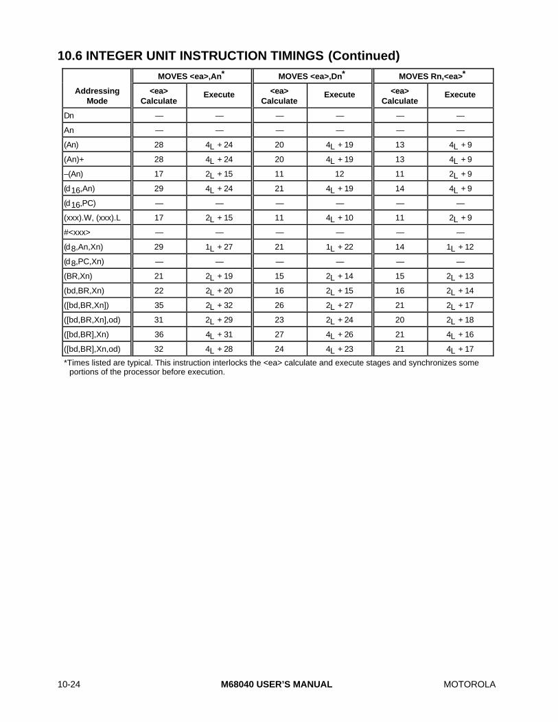
10-24 M68040 USER’S MANUAL MOTOROLA
10.6 INTEGER UNIT INSTRUCTION TIMINGS (Continued)
MOVES <ea>,An* MOVES <ea>,Dn* MOVES Rn,<ea>*
AddressingMode
<ea>Calculate
Execute <ea>Calculate
Execute <ea>Calculate
Execute
Dn — — — — — —
An — — — — — —
(An) 28 4L + 24 20 4L + 19 13 4L + 9
(An)+ 28 4L + 24 20 4L + 19 13 4L + 9
–(An) 17 2L + 15 11 12 11 2L + 9
(d16,An) 29 4L + 24 21 4L + 19 14 4L + 9
(d16,PC) — — — — — —
(xxx).W, (xxx).L 17 2L + 15 11 4L + 10 11 2L + 9
#<xxx> — — — — — —
(d8,An,Xn) 29 1L + 27 21 1L + 22 14 1L + 12
(d8,PC,Xn) — — — — — —
(BR,Xn) 21 2L + 19 15 2L + 14 15 2L + 13
(bd,BR,Xn) 22 2L + 20 16 2L + 15 16 2L + 14
([bd,BR,Xn]) 35 2L + 32 26 2L + 27 21 2L + 17
([bd,BR,Xn],od) 31 2L + 29 23 2L + 24 20 2L + 18
([bd,BR],Xn) 36 4L + 31 27 4L + 26 21 4L + 16
([bd,BR],Xn,od) 32 4L + 28 24 4L + 23 21 4L + 17
*Times listed are typical. This instruction interlocks the <ea> calculate and execute stages and synchronizes someportions of the processor before execution.

MOTOROLA M68040 USER’S MANUAL 10-25
10.6 INTEGER UNIT INSTRUCTION TIMINGS (Continued)
MULS.W/L* MULU.W/L* NBCD
AddressingMode
<ea>Calculate
Execute <ea>Calculate
Execute <ea>Calculate
Execute
Dn 1 16/20 1 14/20 1 3
An — — — — — —
(An) 1 16/20 1 14/20 1 2
(An)+ 1 16/20 1 14/20 1 2
–(An) 1 16/20 1 14/20 1 2
(d16,An) 1/2 16/20 1/2 14/20 1 2
(d16,PC) 3 2L + 16/2L + 20 3 14/20 — —
(xxx).W, (xxx).L 1/2 16/20 1/2 14/20 1 2
#<xxx> 1 16/20 1 14/20 — —
(d8,An,Xn) 3 18/22 3 16/22 3 4
(d8,PC,Xn) 5 1L + 19/1L + 23 5 1L + 17/1L + 23 — —
(BR,Xn) 6 1L + 20/1L + 24 6 1L + 18/1L + 24 6 1L + 6
(bd,BR,Xn) 7 1L + 21/1L + 25 7 1L + 19/1L + 25 7 1L + 7
([bd,BR,Xn]) 9 1L + 23/1L + 27 9 1L + 21/1L + 27 9 1L + 9
([bd,BR,Xn],od) 10 1L + 24/1L + 28 10 1L + 22/1L + 28 10 1L + 10
([bd,BR],Xn) 10 3L + 22/3L + 26 10 3L + 20/3L + 26 10 3L + 8
([bd,BR],Xn,od) 11 3L + 23/3L + 27 11 3L + 21/3L + 27 11 3L + 9
*Multiply <ea> calculate and execute times; T1/T2 apply to word/long-word operand size.

10-26 M68040 USER’S MANUAL MOTOROLA
10.6 INTEGER UNIT INSTRUCTION TIMINGS (Continued)
NEG, NEGX, NOT PEA ROL, ROR
AddressingMode
<ea>Calculate
Execute <ea>Calculate
Execute <ea>Calculate
Execute
Dn 1 1 — — 1 3/4*
An — — — — — —
(An) 1 1 2 1L + 1 1 3
(An)+ 1 1 — — 1 3
–(An) 1 1 — — 1 3
(d16,An) 1 1 2 1L + 1 1 3
(d16,PC) — — 4 3L + 1 — —
(xxx).W, (xxx).L 1 1 2 1L + 1 1 3
#<xxx> — — — — — —
(d8,An,Xn) 3 3 4 1L + 3 3 5
(d8,PC,Xn) — — 6 2L + 4 — —
(BR,Xn) 6 1L + 5 7 2L + 5 6 1L + 7
(bd,BR,Xn) 7 1L + 6 8 2L + 6 7 1L + 8
([bd,BR,Xn]) 9 1L + 8 10 2L + 8 9 1L + 10
([bd,BR,Xn],od) 10 1L + 9 11 2L + 9 10 1L + 11
([bd,BR],Xn) 10 3L + 7 11 4L + 7 10 3L + 9
([bd,BR],Xn,od) 11 3L + 8 12 4L + 8 11 3L + 10
*Immediate count specified for shift count/shift count specified in register, respectively.

MOTOROLA M68040 USER’S MANUAL 10-27
10.6 INTEGER UNIT INSTRUCTION TIMINGS (Continued)
ROXL, ROXR Scc SUBA
AddressingMode
<ea>Calculate
Execute <ea>Calculate
Execute <ea>Calculate
Execute
Dn 1 5/6* 1 2 1 1
An — — — — 1 2
(An) 1 2 1 2 1 2
(An)+ 1 2 1 2 2 1L + 2
–(An) 1 2 1 2 2 1L + 2
(d16,An) 1 2 1 2 2 1L + 2
(d16,PC) — — — — 3 2L + 2
(xxx).W, (xxx).L 1 2 1 2 1 2
#<xxx> — — — — 1 2
(d8,An,Xn) 3 4 4 5 4 5
(d8,PC,Xn) — — — — 5 1L + 5
(BR,Xn) 6 1L + 6 6 1L + 6 6 1L + 6
(bd,BR,Xn) 7 1L + 7 7 1L + 7 7 1L + 7
([bd,BR,Xn]) 9 1L + 9 10 1L + 10 9 1L + 9
([bd,BR,Xn],od) 10 1L + 10 11 1L + 11 10 1L + 10
([bd,BR],Xn) 10 3L + 8 11 3L + 9 10 3L + 8
([bd,BR],Xn,od) 11 3L + 9 12 3L + 10 11 3L + 9
*Immediate count specified for shift count/shift count specified in register, respectively.

10-28 M68040 USER’S MANUAL MOTOROLA
10.6 INTEGER UNIT INSTRUCTION TIMINGS (Concluded)
TAS*
AddressingMode
<ea>Calculate
Execute <ea>Calculate
Execute <ea>Calculate
Execute
Dn 1 2
An — —
(An) 26 2L + 24
(An)+ 26 2L + 24
–(An) 26 2L + 24
(d16,An) 26 2L + 24
(d16,PC) — —
(xxx).W, (xxx).L 26 2L + 24
#<xxx> — —
(d8,An,Xn) 27 27
(d8,PC,Xn) — —
(BR,Xn) 30 1L + 28
(bd,BR,Xn) 31 1L + 29
([bd,BR,Xn]) 33 33
([bd,BR,Xn],od) 35 34
([bd,BR],Xn) 34 3L + 31
([bd,BR],Xn,od) 36 3L + 32
*Times listed are typical. This instruction interlocks the <ea> calculate and execute stages and synchronizes someportions of the processor before execution.

MOTOROLA M68040 USER’S MANUAL 10-29
10.7 FLOATING-POINT UNIT INSTRUCTION TIMINGS
For floating-point instructions in the MC68040, the integer pipeline passes the decodedinstruction to the floating-point unit for execution, then supports the floating-point unit bycalculating effective addresses and transferring operands to and from this unit. For theseinstructions, the execution times listed in the integer unit timing section show the overheadrequired by the integer unit to support the floating-point unit, assuming the floating-pointunit is not busy with the previous floating-point instructions.
Times in parentheses are the total time that that stage uses to execute an instruction eventhough the stage can pass data to the next stage early. The order of operands is generallynot significant for timing purposes. Different rounding modes (i.e., round to zero, etc.)never incur a time penalty. Instructions with an S or D (e.g., FSADD) have the same effectas setting the rounding precision to S or D. All FMOVEM instructions wait for the pipe toidle before starting. Refer to Section 9 Floating-Point Unit (MC68040 Only) for detailson the operation of the floating-point unit pipeline.
10.7.1 Miscellaneous Integer Unit Support Timings
Instruction Condition <ea> Calculate Execute
FBcc TakenNot Taken
76
76
FDBcc cc Truecc False
911
1L + 71L + 9
FNOP FPU Idle 6 6
FTRAPcc Not Taken 6 1L + 5

10-30 M68040 USER’S MANUAL MOTOROLA
10.7.2 Integer Unit Support Timings
FABS, FADD, FCMP, FDIV, FMOVE, FMUL, FNEG, FSQRT, FSUB, FTST <ea>,FPn*
Addressing Byte and Word Long Word Single Precision
Mode <ea>Calculate
Execute <ea>Calculate
Execute <ea>Calculate
Execute
FPn — — — — — —
Dn 2 1L + 2 2 1L + 2 2 1L + 2
(An) 2 2 2 2 2 2
(An)+ 2 2 2 2 2 2
–(An) 2 2 2 2 2 2
(d16,An) 2 2 2 2 2 2
(d16,PC) 4 2L + 2 4 2L + 2 4 2L + 2
(xxx).W, (xxx).L 3 1L + 2 3 1L + 2 3 1L + 2
#<xxx> 5 3L + 2 3 1L + 2 3 1L + 2
(d8,An,Xn) 5 5 5 5 5 5
(d8,PC,Xn) 6 1L + 5 6 1L + 5 6 1L + 5
(An,Xn) 7 1L + 6 7 1L + 6 7 1L + 6
(bd,An,Xn) 8 1L + 7 8 1L + 7 8 1L + 7
([bd,An,Xn]) 11 1L + 10 11 1L + 10 11 1L + 10
([bd,An,Xn],od) 12 1L + 11 12 1L + 11 12 1L + 11
([bd,An],Xn) 12 3L + 9 12 3L + 9 12 3L + 9
([bd,An],Xn,od) 13 3L + 10 13 3L + 10 13 3L + 10
Double Precision Extended Precision
FPn — — 2 1L + 2
Dn — — — —
(An) 2 2 3 3
(An)+ 2 2 3 3
–(An) 2 2 3 3
(d16,An) 2 2 3 3
(d16,PC) 4 1L + 3 5 1L + 4
(xxx).W, (xxx).L 3 1L + 2 4 1L + 3
#<xxx> 4 2L + 2 5 2L + 3
(d8,An,Xn) 5 5 6 6
(d8,PC,Xn) 6 6 7 7
(An,Xn) 7 1L + 6 8 1L + 7
(bd,An,Xn) 8 1L + 7 9 1L + 8
([bd,An,Xn]) 11 1L + 10 12 1L + 11
([bd,An,Xn],od) 12 1L + 11 13 1L + 12
([bd,An],Xn) 12 3L + 9 13 3L + 10
([bd,An],Xn,od) 13 3L + 10 14 3L + 11
*For BR = PC, add one clock to both <ea> calculate and execute times. Timings are for an idle FPU.
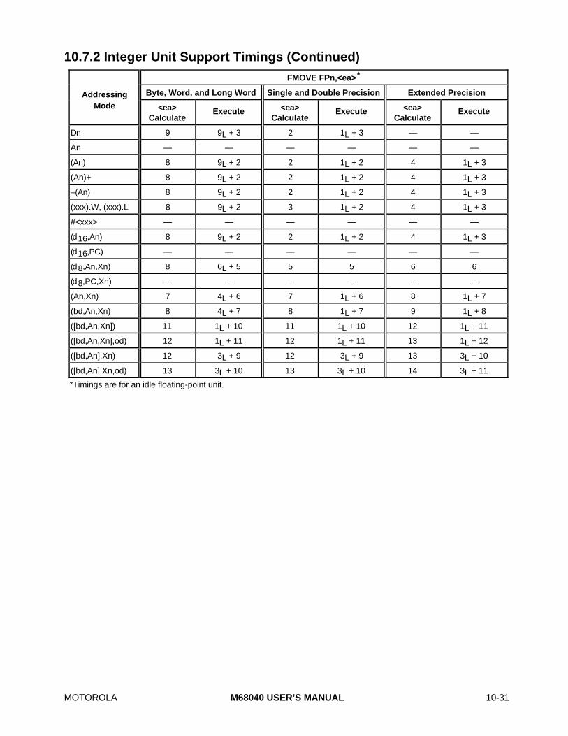
MOTOROLA M68040 USER’S MANUAL 10-31
10.7.2 Integer Unit Support Timings (Continued)
FMOVE FPn,<ea>*
Addressing Byte, Word, and Long Word Single and Double Precision Extended Precision
Mode <ea>Calculate
Execute <ea>Calculate
Execute <ea>Calculate
Execute
Dn 9 9L + 3 2 1L + 3 — —
An — — — — — —
(An) 8 9L + 2 2 1L + 2 4 1L + 3
(An)+ 8 9L + 2 2 1L + 2 4 1L + 3
–(An) 8 9L + 2 2 1L + 2 4 1L + 3
(xxx).W, (xxx).L 8 9L + 2 3 1L + 2 4 1L + 3
#<xxx> — — — — — —
(d16,An) 8 9L + 2 2 1L + 2 4 1L + 3
(d16,PC) — — — — — —
(d8,An,Xn) 8 6L + 5 5 5 6 6
(d8,PC,Xn) — — — — — —
(An,Xn) 7 4L + 6 7 1L + 6 8 1L + 7
(bd,An,Xn) 8 4L + 7 8 1L + 7 9 1L + 8
([bd,An,Xn]) 11 1L + 10 11 1L + 10 12 1L + 11
([bd,An,Xn],od) 12 1L + 11 12 1L + 11 13 1L + 12
([bd,An],Xn) 12 3L + 9 12 3L + 9 13 3L + 10
([bd,An],Xn,od) 13 3L + 10 13 3L + 10 14 3L + 11
*Timings are for an idle floating-point unit.

10-32 M68040 USER’S MANUAL MOTOROLA
10.7.2 Integer Unit Support Timings (Continued)
AddressingFMOVE/FMOVEM to/from
1 Control RegisteraFMOVEM <list>,<ea>and <ea>,<list>a,b FScca
Mode <ea>Calculate
Execute <ea>Calculate
Execute <ea>Calculate
Execute
Dn 2 1L + 2 — — 5 6
An 2 1L + 2 — — — —
(An) 4 2L + 3 17 2L + 15 4 5
(An)+ 4 2L + 3 17 2L + 15 6 2L + 5
–(An) 5 3L + 3 16 1L + 15 6 2L + 5
(xxx).W, (xxx).L 4 2L + 3 19 3L + 15 4 5
#<xxx> 4 2L + 3 19 1L + 17 — —
(d16,An) 4 2L + 3 17 2L + 15 4 5
(d16,PC) 5 4L + 3 — — — —
(d8,An,Xn) 5 6 19 18 7 8
(d8,PC,Xn) 6 1L + 6 20 1L + 18 — —
(An,Xn) 7 1L + 7 20 1L + 19 9 1L + 9
(bd,An,Xn) 8 1L + 8 21 1L + 20 10 1L + 10
([bd,An,Xn]) 11 1L + 11 25 1L + 23 13 1L + 13
([bd,An,Xn],od) 12 1L + 13 25 1L + 24 14 1L + 14
([bd,An],Xn) 12 3L + 10 26 3L + 22 14 3L + 12
([bd,An],Xn,od) 13 3L + 12 26 3L + 23 15 3L + 13NOTES:
a. Timings are for an idle floating-point unit. Same as FMOVE <ea>,FPCR.b. Add three clocks to both <ea> calculate and execute times for each additional floating-point register. Add one
clock to both <ea> calculate and execute times for dynamic register list.

MOTOROLA M68040 USER’S MANUAL 10-33
10.7.2 Integer Unit Support Timings (Continued)
FSAVE <ea>*
Addressing Idle or Null Short Long
Mode <ea>Calculate
Execute <ea>Calculate
Execute <ea>Calculate
Execute
FPn — — — — — —
Dn — — — — — —
An — — — — — —
(An) 12 1L + 11 33 1L + 32 50 1L + 49
(An)+ — — — — — —
–(An) 11 11 32 32 49 49
(xxx).W, (xxx).L 13 1L + 11 34 1L + 32 51 1L + 49
#<xxx> — — — — — —
(d16,An) 12 1L + 11 33 1L + 32 50 1L + 49
(d16,PC) — — — — — —
(d8,An,Xn) 13 13 34 34 51 51
(d8,PC,Xn) — — — — — —
(An,Xn) 16 1L + 14 37 1L + 35 54 1L + 52
(bd,An,Xn) 17 1L + 15 38 1L + 36 55 1L + 53
([bd,An,Xn]) 19 1L + 18 40 1L + 39 57 1L + 56
([bd,An,Xn],od) 21 1L + 19 42 1L + 40 59 1L + 57
([bd,An],Xn) 20 3L + 17 41 3L + 38 58 3L + 55
([bd,An],Xn,od) 22 3L + 18 46 3L + 42 65 3L + 61
*Timings are for an idle floating-point unit.

10-34 M68040 USER’S MANUAL MOTOROLA
10.7.2 Integer Unit Support Timings (Concluded)
FRESTORE <ea>*
Addressing Idle or Null Short Long
Mode <ea>Calculate
Execute <ea>Calculate
Execute <ea>Calculate
Execute
FPn — — — — — —
Dn — — — — — —
An — — — — — —
(An) 13 1L + 12 26 1L + 25 40 1L + 39
(An)+ 13 1L + 12 26 1L + 25 40 1L + 39
–(An) — — — — — —
(d16,An) 13 1L + 12 26 1L + 25 40 1L + 39
(d16,PC) — — — — — —
(xxx).W, (xxx).L 14 1L + 12 27 1L + 25 41 1L + 39
#<xxx> — — — — — —
(d8,An,Xn) 14 14 27 27 41 41
(d8,PC,Xn) — — — — — —
(An,Xn) 16 1L + 14 29 1L + 27 43 1L + 41
(bd,An,Xn) 17 1L + 15 30 1L + 28 44 1L + 42
([bd,An,Xn]) 20 1L + 19 33 1L + 32 47 1L + 46
([bd,An,Xn],od) 21 1L + 19 34 1L + 32 48 1L + 46
([bd,An],Xn) 21 3L + 18 34 3L + 31 48 3L + 45
([bd,An],Xn,od) 22 3L + 19 35 3L + 31 49 3L + 45
*Timings are for an idle floating-point unit.

MOTOROLA M68040 USER’S MANUAL 10-35
10.7.3 Timings in the Floating-Point Unit
Times in parentheses are the total time that the stage uses to execute an instruction eventhough the stage can pass data to the next stage earlier. So that 2(3) in the conversionstage means that the instruction takes two cycles to execute, but this stage is actuallybusy for three cycles.
Instruction Opclass Size Precision Operands Conversion Execution Normalization
FADD,FSUB 0 — Any Norm,Norm 2(3) 3 2(3)
0 — Any Norm,Zero 2(3) 3 2(3)
0 — Any Zero,Zero 4 0 0
0 — Any — ,Inf 4 0 0
0 — Any — ,NAN 4 0 0
0 S,D Any Norm,Norm 2(3) 3 2(3)
2 S,D Any Norm,Zero 2(3) 3 2(3)
2 S,D Any Zero,Zero 4 0 0
2 S,D Any — ,Inf 4 0 0
2 S,D Any — ,NAN 4 0 0
2 X Any Norm,Norm 3(4) 3 2(3)
2 X Any Norm,Zero 3(4) 3 2(3)
2 X Any Zero,Zero 5 0 0
2 X Any — ,Inf 5 0 0
2 X Any — ,NAN 5 0 0
FMUL 0 — Any Norm,Norm 2(3) 5 2(3)
0 — Any — ,Zero 4 0 0
0 — Any — ,Inf 4 0 0
0 — Any — ,NAN 4 0 0
2 S,D Any Norm,Norm 2(3) 5 2(3)
2 S,D Any — ,Zero 4 0 0
2 S,D Any — ,Inf 4 0 0
2 S,D Any — ,NAN 4 0 0
2 X Any Norm,Norm 3(4) 5 2(3)
2 X Any — ,Zero 5 0 0
2 X Any — ,Inf 5 0 0
2 X Any — ,NAN 5 0 0
FDIV 0 Any Norm,Norm 2(3) 37.5 2(3)
0 — Any — ,Zero 4 0 0
0 — Any — ,Inf 4 0 0
0 — Any — ,NAN 4 0 0
2 S,D Any Norm,Norm 2(3) 37.5 2(3)
2 S,D Any — ,Zero 4 0 0
2 S,D Any — ,Inf 4 0 0

10-36 M68040 USER’S MANUAL MOTOROLA
10.7.3 Timings in the Floating-Point Unit (Continued)
Instruction Opclass Size Precision Operands Conversion Execution Normalization
FDIV 2 S,D Any — ,NAN 4 0 0
2 X Any Norm,Norm 3(4) 37.5 2(3)
2 X Any — ,Zero 5 0 0
2 — Any — ,Inf 5 0 0
2 X Any — ,NAN 5 0 0
FSQRT 0 — Any Norm 2(3) 103 2(3)
0 — Any (Zero|Inf|NAN) 4 0 0
2 S,D Any Norm 2(3) 103 2(3)
2 S,D Any (Zero|Inf|NAN) 4 0 0
2 X Any Norm 3(4) 103 2(3)
2 X Any (Zero|Inf|NAN) 5 0 0
FMOVE, 0 — X (Norm|Zero|Inf) 2 0 0
FABS, 0 — X NAN 3 0 0
FNEG 0 — S,D Norm 5 0 0
0 — S,D (Zero|Inf) 3 0 0
0 — S,D NAN 4 0 0
2 S Any (Norm|Zero|Inf) 3 0 0
2 S Any NAN 4 0 0
2 D D,X (Norm|Zero|Inf) 3 0 0
2 D D,X NAN 4 0 0
2 D S Norm 5 0 0
2 D S (Zero|Inf) 4 0 0
2 D S NAN 5 0 0
2 X X (Norm|Zero|Inf) 4 0 0
2 X X NAN 5 0 0
2 X S,D Norm 6 0 0
2 X S,D (Zero|Inf) 5 0 0
2 X S,D NAN 6 0 0
2 B,W Any (+Norm|Zero) 1.5(11) 4.5 2
2 L D,X (+Norm|Zero) 1.5(11) 4.5 2
2 L S (+Norm|Zero) 1.5(12.5) 4.5 2
2 B,W Any —Norm 1.5(11.5) 5 2
2 L D,X —Norm 1.5(11.5) 5 2
2 L S —Norm 1.5(13) 5 2
FMOVE 3 S,D Any Any 3 0 0
3 X Any Any 4 0 0
3 B,W,L Any +(Norm|Zero) 3(9) 1.5 3.5
3 B,W,L Any –(Norm|Zero) 3(10) 1.5 4.5
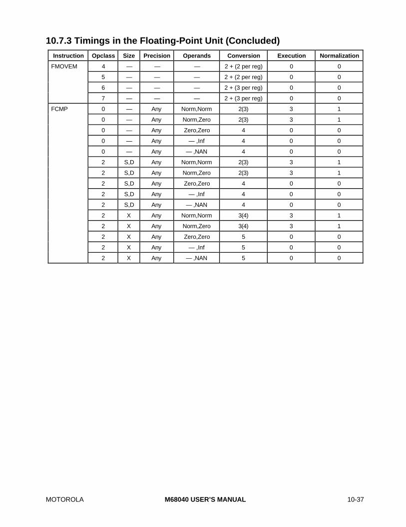
MOTOROLA M68040 USER’S MANUAL 10-37
10.7.3 Timings in the Floating-Point Unit (Concluded)
Instruction Opclass Size Precision Operands Conversion Execution Normalization
FMOVEM 4 — — — 2 + (2 per reg) 0 0
5 — — — 2 + (2 per reg) 0 0
6 — — — 2 + (3 per reg) 0 0
7 — — — 2 + (3 per reg) 0 0
FCMP 0 — Any Norm,Norm 2(3) 3 1
0 — Any Norm,Zero 2(3) 3 1
0 — Any Zero,Zero 4 0 0
0 — Any — ,Inf 4 0 0
0 — Any — ,NAN 4 0 0
2 S,D Any Norm,Norm 2(3) 3 1
2 S,D Any Norm,Zero 2(3) 3 1
2 S,D Any Zero,Zero 4 0 0
2 S,D Any — ,Inf 4 0 0
2 S,D Any — ,NAN 4 0 0
2 X Any Norm,Norm 3(4) 3 1
2 X Any Norm,Zero 3(4) 3 1
2 X Any Zero,Zero 5 0 0
2 X Any — ,Inf 5 0 0
2 X Any — ,NAN 5 0 0

10-38 M68040 USER’S MANUAL MOTOROLA

MOTOROLA M68040 USER’S MANUAL 11-1
This device contains protectivecircuitry against damage due to highstatic voltages or electrical fields;however, it is advised that normalprecautions be taken to avoidapplication of any voltages higherthan maximum-rated voltages to thishigh-impedance circuit. Reliablity ofoperation is enhanced if unusedinputs are tied to an appropriatelogic voltage level (e.g., either GNDor VCC).
SECTION 11MC68040 ELECTRICAL ANDTHERMAL CHARACTERISTICS
The following paragraphs provide information on the maximum rating and thermalcharacteristics for the MC68040. This section is subject to change. For the most recentspecifications, contact a Motorola sales office or complete the registration card at the endof this manual.
11.1 MAXIMUM RATINGS
Characteristic Symbol Value Unit
Supply Voltage VCC –0.3 to +7.0 V
Input Voltage Vin –0.5 to +7.0 V
Maximum Operating Junction Temperature TJ 110 °C
Minimum Operating Ambient Temperature TA 0 °C
Storage Temperature Range Tstg –55 to 150 °C
11.2 THERMAL CHARACTERISTICS
Characteristic Symbol Value Rating
Thermal Resistance, Junction to Case—PGA Package
θJC 3 °C/W

11-2 M68040 USER’S MANUAL MOTOROLA
11.3 DC ELECTRICAL SPECIFICATIONS (VCC = 5.0 VDC ±5 %)
Characteristic Symbol Min Max Unit
Input High Voltage VIH 2 VCC V
Input Low Voltage VIL GND 0.8 V
Undershoot — — 0.8 V
Input Leakage Current @ 0.5/2.4 VAVEC , BCLK, BG, CDIS , MDIS, IPL≈, PCLK, RSTI, SCx,TBI, TLNx , TCI , TCK, TEA
Iin 20 20 µA
Hi-Z (Off-State) Leakage Current @ 0.5/2.4 VAn, BB, CIOUT , Dn, LOCK , LOCKE, R/ W , SIZx, TA, TDO,TIP, TMx, TLNx, TS, TTx, UPAx
ITSI 20 20 µA
Signal Low Input Current, VIL = 0.8 VTMS, TDI, TRST
IIL –1.1 –0.18 mA
Signal High Input Current, VIH = 2.0 VTMS, TDI, TRST
IIH –0.94 –0.16 mA
Output High Voltage, IOH = 5 mA (Small Buffer Mode) VOH 2.4 — V
Output Low Voltage, IOL = 5 mA (Small Buffer Mode) VOL — 0.5 V
Output High Voltage, IOH = 55 mA (Large Buffer Mode) VOH 2.4 — V
Output Low Voltage, IOL = 55 mA (Large Buffer Mode) VOL — 0.5 V
Capacitance*, Vin = 0 V, f = 1 MHz Cin — 25 pF
*Capacitance is periodically sampled rather than 100% tested.
11.4 POWER DISSIPATION
Buffer Mode 25 MHz 33 MHz 40 MHz
Worst Case (VCC = 5.25 V , TA = 0°C)
Small Unterminated, IOL = IOH = 5 mA 4.9 W 6.2 W 7.2 W
Large Unterminated, IOL = IOH = 5 mA 5.1 W 6.6 W 7.7 W
Large Terminated, 50 Ω, 2.5 V, IOL = IOH = 55 mA 6.5 W 8.0 W 9.1 W
Typical Values (VCC = 5 V, TJ = 90°C)*
Small 3.0 W 4.1 W 4.5 W
Large Unterminated 3.3 W 4.4 W 4.8 W
Large Terminated, 50 Ω, 2.5 V 4.7 W 5.8 W 6.2 W
*This information is for system reliability purposes.

MOTOROLA M68040 USER’S MANUAL 11-3
11.5 CLOCK AC TIMING SPECIFICATIONS (see Figure 11-1)
25 MHz 33 MHz 40 MHz
Num Characteristic Min Max Min Max Min Max Unit
Frequency of Operation 20 25 20 33 20 40 MHz
1 PCLK Cycle Time 20 25 15 25 12.5 25 ns
2 PCLK Rise Time — 1.7 — 1.7 — 1.5 ns
3 PCLK Fall Time — 1.6 — 1.6 — 1.5 ns
4 PCLK Duty Cycle Measured at 1.5 V 47.50 52.50 46.67 53.33 46.00 54.00 %
4a* PCLK Pulse Width High Measured at 1.5 V 9.50 10.50 7 8 5.75 6.75 ns
4b* PCLK Pulse Width Low Measured at 1.5 V 9.50 10.50 7 8 5.75 6.75 ns
5 BCLK Cycle Time 40 60 30 60 25 50 ns
6,7 BCLK Rise and Fall Time — 4 — 3 — 3 ns
8 BCLK Duty Cycle Measured at 1.5 V 40 60 40 60 40 60 %
8a* BCLK Pulse Width High Measured at 1.5 V 16 24 12 18 10 15 ns
8b* BCLK Pulse Width Low Measured at 1.5 V 16 24 12 18 10 15 ns
9 PCLK, BCLK Frequency Stability — 1000 — 1000 — 1000 ppm
10 PCLK to BCLK Skew — 9 — n/a — n/a ns
*Specification value at maximum frequency of operation.
2 31
5
6 71010
PCLK
BCLK
8B8A
4A 4B
VMV
V
IH
IL
VIH
VILVM
Figure 11-1. Clock Input Timing Diagram

11-4 M68040 USER’S MANUAL MOTOROLA
11.6 OUTPUT AC TIMING SPECIFICATIONS (See Figures 11-3 to 11-7)
25 MHz 33 MHz 40 Mhz
Large1 Small2 Large1 Small2 Large1 Small2
Num Characteristic Min Max Min Max Min Max Min Max Min Max Min Max Unit
113 BCLK to Address CIOUT, LOCK ,LOCKE, R/W , SIZx, TLN, TMx, TTx,UPAx Valid
9 21 9 30 6.50 18 6.50 25 5.25 16 5.25 24 ns
12 BCLK to Output Invalid(Output Hold)
9 — 9 — 6.50 — 6.50 — 5.25 — 5.25 — ns
13 BCLK to TS Valid 9 21 9 30 6.50 18 6.50 25 5.25 16 5.25 24 ns
14 BCLK to TIP Valid 9 21 9 30 6.50 18 6.50 25 5.25 17 5.25 24 ns
184 BCLK to Data Out Valid 9 23 9 32 6.50 20 6.50 27 5.25 18 5.25 26 ns
194 BCLK to Data Out Invalid (OutputHold)
9 — 9 — 6.50 — 6.50 — 5.25 — 5.25 — ns
203,4 BCLK to Output Low Impedance 9 — 9 — 6.50 — 6.50 — 5.25 — 5.25 — ns
215 BCLK to Data-Out High Impedance 9 20 9 20 6.50 17 6.50 17 5.25 16 5.25 16 ns
263 BCLK to MultiplexedAddress Valid
19 31 19 40 14 26 14 33 13 25 13 32 ns
273,5 BCLK to MultiplexedAddress Driven
19 — 19 — 14 — 14 — 13 — 13 — ns
283,4,5 BCLK to Multiplexed AddressHigh Impedance
9 18 9 18 6.50 15 6.50 15 5.25 14 5.25 14 ns
294,5 BCLK to MultiplexedData Driven
19 — 19 — 14 20 14 20 13 19 13 19 ns
304 BCLK to Multiplexed Data Valid 19 33 19 42 14 28 14 35 13 27 13 34 ns
383 BCLK to Address, CIOUT , LOCK,LOCKE, R/W , SIZx, TS, TLNx, TMx,TTx, UPAx High Impedance
9 18 9 18 6.50 15 6.50 15 5.25 14 5.25 14 ns
39 BCLK to BB, TA, TIP
High Impedance19 28 19 28 14 23 14 23 11.5 22 11.5 22 ns
40 BCLK to BR , BB Valid 9 21 9 30 6.50 18 6.50 25 5.25 16 5.25 24 ns
43 BCLK to MI Valid 9 21 9 30 6.50 18 6.50 25 5.25 17 5.25 24 ns
48 BCLK to TA Valid 9 21 9 30 6.50 18 6.50 25 5.25 17 5.25 24 ns
50 BCLK to IPEND, PSTx, RSTO Valid 9 21 9 30 6.50 18 6.50 25 5.25 17 5.25 24 ns
NOTES:1. Output timing is specified for a valid signal measured at the pin. Large buffer timing is specified driving a 50 Ω
transmission line with a length characterized by a 2.5-ns one-way propagation delay, terminated through 50 Ω to2.5 V. Large buffer output impedance is 4–12 Ω, resulting in incident wave switching for this environment. Alllarge buffer outputs must be terminated to guarantee operation.
2. Small buffer timing is specified driving an unterminated 30 Ω transmission line with a length characterized by a2.5 ns one-way propagation delay. Small buffer output impedance is typically 30 Ω; the small buffer specificationsinclude approximately 5 ns for the signal to propagate the length of the transmission line and back.
3. Timing specifications 11, 20, and 38 for address bus output timing apply when normal bus operation is selected.Specifications 26, 27, and 28 should be used when the multiplexed bus mode of operation is enabled.
4. Timing specifications 18 and 19 for data bus output timing apply when normal bus operation is selected.Specifications 28 and 29 should be used when the multiplexed bus mode of operation is enabled.
5. Timing specifications 21, 27, 28, and 29 are measured from BCLK edges. By design, the MC68040 cannot driveaddress and data simultaneously during multiplexed operations.
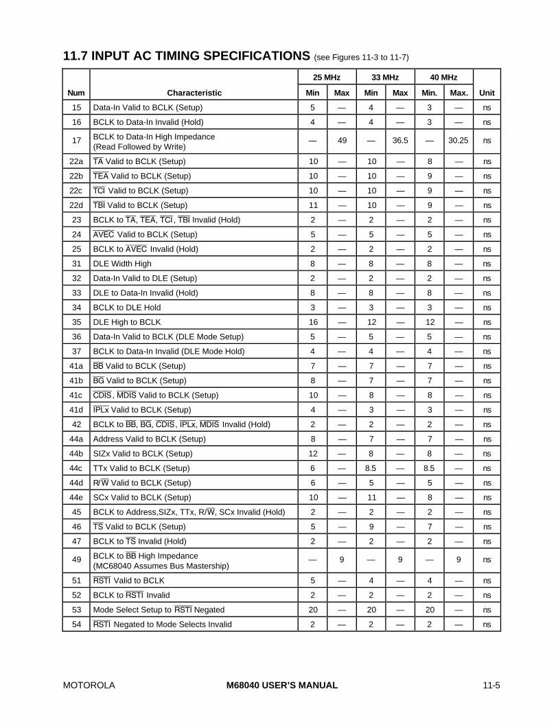
MOTOROLA M68040 USER’S MANUAL 11-5
11.7 INPUT AC TIMING SPECIFICATIONS (see Figures 11-3 to 11-7)
25 MHz 33 MHz 40 MHz
Num Characteristic Min Max Min Max Min. Max. Unit
15 Data-In Valid to BCLK (Setup) 5 — 4 — 3 — ns
16 BCLK to Data-In Invalid (Hold) 4 — 4 — 3 — ns
17 BCLK to Data-In High Impedance(Read Followed by Write)
— 49 — 36.5 — 30.25 ns
22a TA Valid to BCLK (Setup) 10 — 10 — 8 — ns
22b TEA Valid to BCLK (Setup) 10 — 10 — 9 — ns
22c TCI Valid to BCLK (Setup) 10 — 10 — 9 — ns
22d TBI Valid to BCLK (Setup) 11 — 10 — 9 — ns
23 BCLK to TA, TEA, TCI , TBI Invalid (Hold) 2 — 2 — 2 — ns
24 AVEC Valid to BCLK (Setup) 5 — 5 — 5 — ns
25 BCLK to AVEC Invalid (Hold) 2 — 2 — 2 — ns
31 DLE Width High 8 — 8 — 8 — ns
32 Data-In Valid to DLE (Setup) 2 — 2 — 2 — ns
33 DLE to Data-In Invalid (Hold) 8 — 8 — 8 — ns
34 BCLK to DLE Hold 3 — 3 — 3 — ns
35 DLE High to BCLK 16 — 12 — 12 — ns
36 Data-In Valid to BCLK (DLE Mode Setup) 5 — 5 — 5 — ns
37 BCLK to Data-In Invalid (DLE Mode Hold) 4 — 4 — 4 — ns
41a BB Valid to BCLK (Setup) 7 — 7 — 7 — ns
41b BG Valid to BCLK (Setup) 8 — 7 — 7 — ns
41c CDIS , MDIS Valid to BCLK (Setup) 10 — 8 — 8 — ns
41d IPL≈ Valid to BCLK (Setup) 4 — 3 — 3 — ns
42 BCLK to BB, BG, CDIS , IPL≈, MDIS Invalid (Hold) 2 — 2 — 2 — ns
44a Address Valid to BCLK (Setup) 8 — 7 — 7 — ns
44b SIZx Valid to BCLK (Setup) 12 — 8 — 8 — ns
44c TTx Valid to BCLK (Setup) 6 — 8.5 — 8.5 — ns
44d R/W Valid to BCLK (Setup) 6 — 5 — 5 — ns
44e SCx Valid to BCLK (Setup) 10 — 11 — 8 — ns
45 BCLK to Address,SIZx, TTx, R/W, SCx Invalid (Hold) 2 — 2 — 2 — ns
46 TS Valid to BCLK (Setup) 5 — 9 — 7 — ns
47 BCLK to TS Invalid (Hold) 2 — 2 — 2 — ns
49 BCLK to BB High Impedance(MC68040 Assumes Bus Mastership)
— 9 — 9 — 9 ns
51 RSTI Valid to BCLK 5 — 4 — 4 — ns
52 BCLK to RSTI Invalid 2 — 2 — 2 — ns
53 Mode Select Setup to RSTI Negated 20 — 20 — 20 — ns
54 RSTI Negated to Mode Selects Invalid 2 — 2 — 2 — ns

11-6 M68040 USER’S MANUAL MOTOROLA
B
ADRIVE TO 0.5 V
2.0 V
0.8 V
VALID OUTPUT n
VALID OUTPUT n + 1
2.0 V0.8 V
VALID INPUT
2.0 V
0.8 V
2.0 V
0.8 V
DC
DRIVE TO 0.5 V
DRIVE TO 2.4 V
2.0 V
2.0 V
0.8 V
E
F
BCLK
OUTPUTS(1)
INPUTS(2)
RSTI (3)
NOTES:1. This output timing is applicable to all parameters specified relative to the rising edge of the clock.2. This input timing is applicable to all parameters specified relative to the rising edge of the clock.3. This timing is applicable to all parameters specified relative to the negation of the RSTI signal.
LEGEND:
A. Maximum output delay specification. B. Minimum output hold time. C. Minimum input setup time specification. D. Minimum input hold time specification. E. Mode select setup time to RSTI negated.F. Mode select hold time from RSTI negated.
DRIVE TO 2.4 V
1.5 V 1.5 V
IPLx, CDIS, MDIS
Figure 11-2. Drive Levels and Test Points for AC Specifications

MOTOROLA M68040 USER’S MANUAL 11-7
2223
11
BCLK
A31–A0
TRANSFER ATTRIBUTES
D31–D0 IN (READ)
12
1516
D31–D0 OUT (WRITE)
1921
13 12
14
18
20
TA
TEA
TCI
TBI
TIP
TS
NOTE: Transfer Attribute Signals = UPAx, SIZx, TTx, TMx, TLNx, R/W, LOCK, LOCKE, CIOUT
AVEC
2425
12
Figure 11-3. Read/Write Timing

11-8 M68040 USER’S MANUAL MOTOROLA
BCLK
A31–A0
TRANSFER ATTRIBUTES
38
20
11
TS
TIP
BB OUT12
39
BG
BR
41 42
12
21
D31–D0 OUT (WRITE)
20
40
13
14
MI
4312
1239
40
NOTE: Transfer Attribute Signals = UPAx, SIZx, TTx, TMx, TLNx, R/W, CIOUT
LOCK, LOCKE
Figure 11-4. Bus Arbitration Timing

MOTOROLA M68040 USER’S MANUAL 11-9
D31–D0 IN (ALT. MASTER
WRITE)
D31–D0 OUT (ALT. MASTER
READ)
44
BCLK
A31–A0 IN
15 16
4647
12
4148
1220 39
4249
43
1921
18
TS IN
MI
TA OUT
BB IN
SIZx, TTx, R/W IN
45
SC1, SC0
Figure 11-5. Snoop Hit Timing

11-10 M68040 USER’S MANUAL MOTOROLA
TBI
TS IN
MI
SIZx, TTx, R/W IN
44
BCLK
A31–A0 IN
TEA
4647
SC1,SC0 SNOOP
43
TA
45
2223
BB IN41
42
43
12
Figure 11-6. Snoop Miss Timing
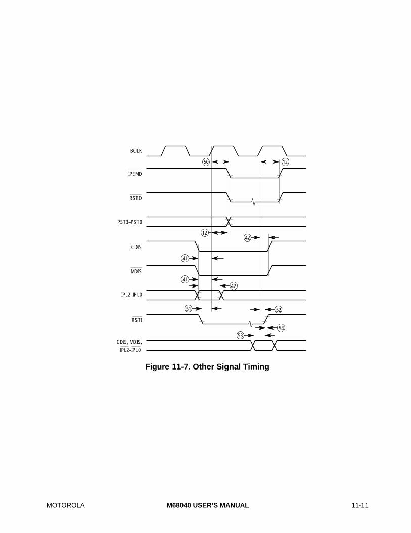
MOTOROLA M68040 USER’S MANUAL 11-11
50
BCLK
12
42
41
IPEND
RSTO
CDIS
MDIS
IPL2–IPL0
42
PST3–PST0
12
54
RSTI
CDIS, MDIS,
51 52
IPL2–IPL0
53
41
Figure 11-7. Other Signal Timing
11-12 M68040 USER’S MANUAL MOTOROLA
11.8 MC68040 THERMAL DEVICE CHARACTERISTICS
The need to efficiently cool microprocessors is becoming more important as they becomemore complex and require more power. In the past, the M68000 family has been able toprovide a 0–70°C ambient temperature part for speeds less than 40 MHz. However, theMC68040, MC68LC040, and MC68EC040 with a 50 MHz processor clock has a maximumpower dissipation for a particular operating mode, a maximum junction temperature, and athermal resistance from the die junction to the case. This section provides a moreaccurate method of evaluating the environment, taking into consideration both the airflowand ambient temperature. This section also gives the user information to design a coolingmethod that meets both thermal performance requirements and constraints of the boardenvironment. This section discusses the device characteristics and several methods forthermal management as well as an example of one method for cooling the MC68040,MC68LC040, and MC68EC040. The MC68040, MC68LC040, and MC68EC040 containinherent characteristics that should be considered when evaluating a method for coolingthe device. The following paragraphs discuss these die/package and powerconsiderations for each of these parts.
NOTE
All references to the MC68040 also include the MC68LC040and MC68EC040. Note that the MC68LC040 and MC68EC040only implement the small buffer mode.
11.8.1 MC68040 Die and PackageThe MC68040 is in a cavity-down alumina-ceramic 179-pin PGA that has a worst casethermal resistance from junction to case of 3°C/W. The package differs from previousM68000 family PGA packages that are cavity-up. The cavity-down design allows the die tobe attached to the top surface of the package, increasing the part’s ability to dissipate heatthrough the package surface or an attached heat sink. The system designer needs todetermine the specific dimensions and design of the particular heat sink, considering boththermal performance and size requirements.
11.8.2 MC68040 Power ConsiderationsThe MC68040 has a maximum power rating, which varies depending on the combinationof output buffer mode and operating frequency. Note that this section assumes largebuffers terminated to 2.5 V. The large buffer output mode dissipates more power than thesmall, and higher frequencies of operation dissipate more power than the lowerfrequencies.
The MC68040 allows a combination of either large or small buffers on the outputs of themiscellaneous control signals, data bus, and address bus/transfer attribute pins. The largebuffers offer quicker output times, allowing for an easier logic design. However, they do soby driving about 10 times as much current as the small buffers. The designer shouldconsider whether the quicker timings present enough advantage to justify the additionalconsideration to the individual signal terminations, the die power consumption, and therequired cooling for the device. Since the MC68040 can be powered up in one of manyoutput buffer modes upon reset, the actual maximum power consumption for an MC68040

MOTOROLA M68040 USER’S MANUAL 11-13
rated at a particular maximum operating frequency is dependent upon the power-upmode. Therefore, the MC68040 is rated at a maximum power dissipation for either thelarge or small buffers at a particular frequency. This allows for control of some of thethermal management upon reset. The following equation provides a rough method tocalculate the maximum power consumption for a chosen output buffer mode:
PD = PDSB + (PDLB – PDSB) × ( PINSLB ÷ PINSCLB)
where:PD = Maximum Power Dissipation for Output Buffer Mode Selected
PDSB = Maximum Power Dissipation for Small Buffer Mode (All Outputs)PDLB = Maximum Power Dissipation for Large Buffer Mode (All Outputs)
PINSLB = Number of Pins Large Buffer ModePINSCLB = Number of Pins Capable of the Large Buffer Mode
Table 11-1 lists the simplified relationship on the maximum power dissipation for eightpossible configurations of output buffer modes.
Table 11-1. Maximum Power Dissipation for Output Buffer Mode Configurations
Output Configuration
Data BusAddress Bus and
Transfer Attributes Control Signals Maximum Power Dissipation
Small* Small Small PDSB
Small Small Large PDSB + (PDLB – PDSB) × 13%
Small Large Small PDSB + (PDLB – PDSB) × 52%
Small Large Large PDSB + (PDLB – PDSB) × 65%
Large Small Small PDSB + (PDLB – PDSB) × 35%
Large Small Large PDSB + (PDLB – PDSB) × 48%
Large Large Small PDSB + (PDLB – PDSB) × 87%
Large Large Large PDSB + (PDLB – PDSB) × 100%
*The MC68LC040 and MC68EC040 only utilize this row of information.
To calculate the specific power dissipation of a design, the termination method of eachsignal must be considered. For example, a signal output that is not connected would notdissipate any additional power if it were configured in the large rather than the small buffermode. Since the maximum operating junction temperature is specified as 110°C, themaximum case temperature (TC) in °C can be obtained from the following equation:
TC = TJ – PD × θJC
where:TC = Maximum Case TemperatureTJ = Maximum Junction TemperaturePD = Maximum Power Dissipation of the DeviceθJC = Thermal Resistance between the Junction of the Die and the Case
11-14 M68040 USER’S MANUAL MOTOROLA
In general, the ambient temperature (TA ) in °C is a function of the following equation:
TA = TJ – PD × θJC – PD × θCA
The thermal resistance from case to outside ambient (θCA) is the only user-dependentparameter once a buffer output configuration has been determined. Reducing the case toambient thermal resistance increases the maximum operating ambient temperature.Therefore, by utilizing methods such as heat sinks and ambient air cooling to minimizeθCA, a higher ambient operating temperature and/or a lower junction temperature can beachieved. However, an easier approach to thermal evaluation uses the followingequations:
TA = TJ – PD × θJA or TJ = TA + PD × θJA
where:θJA = Thermal Resistance from the Junction to the Ambient (θJC + θCA)
The total thermal resistance for a package (θJA) is a combination of its two components,θJC and θCA. These components represent the barrier to heat flow from the semiconductorjunction to the package case surface (θJC) and θCA. Although θJC is package related andthe user cannot influence it, θCA is user dependent. Good thermal management by theuser, such as heat sink and airflow, can significantly reduce θCA achieving either a lowersemiconductor junction temperature or a higher ambient operating temperature.
11.9 MC68040 THERMAL MANAGEMENT TECHNIQUES
To attain a reasonable maximum ambient operating temperature, the user must reducethe barrier to heat flow from θJA. The only way to accomplish this is to significantly reduceθCA by applying thermal management techniques such as heat sinks and forced aircooling. The following paragraphs discuss thermal study results for the MC68040 that didnot use thermal management techniques, airflow cooling, heat sink, and heat sinkcombined with airflow cooling.
The MC68040 power dissipation values given in this section represent the sum of thepower dissipated by the internal circuitry and the output buffers of the MC68040. Thetermination network chosen by the system designer strongly influences this lastcomponent of power. Values listed in this section for large buffer terminated entries reflecta termination network as illustrated in Figure 11-8 and are consistent with specificationsfor the MC68040. For additional termination schemes, refer to AN1051, Transmission LineEffects in PCB Applications, or AN1061, Reflecting on Transmission Line Effects.

MOTOROLA M68040 USER’S MANUAL 11-15
2.5 V
R = 5050 Ω T.L.
MC68040 OUTPUT BUFFER
TYPICAL Z = 4–12 Ω (LARGE)0 TYPICAL Z = 25 Ω (SMALL)0
Ω
Figure 11-8. MC68040 Termination Network
If a designer uses alternative standard termination methods, such as RC terminationnetwork (see Figure 11-9), Thévenin termination network (not illustrated), or notermination method at all, which is not recommended, then the power dissipation of theMC68040 will be significantly less than the large buffer terminated values. For terminationnetworks other than that illustrated in Figure 11-31, the designer must calculate thecomponent of power dissipated in the output buffer and add this value to the small bufferunterminated value.
C = 300 pF
R = 5050 Ω T.L.
MC68040 OUTPUT BUFFER Ω
TYPICAL Z = 4–12 Ω (LARGE)0 TYPICAL Z = 25 Ω (SMALL)0
Figure 11-9. Typical Configuration for RC Termination Network
The following paragraphs describe how the large buffer terminated values werecalculated. The MC68040 termination network causes current flow through the outputbuffer of the MC68040, regardless of whether the MC68040 is driving a logic one or alogic zero. The following equation gives the large buffer termination network powerdissipation for a given pin:
I = (V ÷ (R + Zo)) + 5 mA
P = I2Reff
Reff is the effective average output resistance, including typical pullup resistance, typicalpulldown resistance, and a duty cycle average of how often the pin is high, low, or three-stated. Typical values for Zo are 6 Ω for large buffer low output, 12 Ω for large buffer highoutput, and 25 Ω for small buffer output. Using these values and duty cycle assumptionsbased on sequential burst write cycles, Reff calculates to 7.7 Ω for the MC68040 largebuffer mode and 25 Ω for the small buffer mode.
Maximum termination current in the large buffer mode occurs for output:
Low: Itl = (2.5 V ÷ (50 + 6 Ω)) + 5 mA = 49.6 mA
High: Ith = (2.75 V ÷ (50 + 12 Ω)) + 5 mA = 50.8 mA

11-16 M68040 USER’S MANUAL MOTOROLA
Maximum power dissipation in the large buffer mode occurs for output:
Low: Pllb = I2R = (49.6 mA)2 x 6 Ω = 14.8 mW
High: Phlb = I2R = (50.8 mA)2 x 12 Ω = 30.1 mW
Similar calculations for unterminated small buffers yield:
I = 5 mA (by spec)and
P = I2R = (5 mA)2 x 25 Ωso
Phsb = 0.625 mWPlsb = 0.625 mW
Assuming that the duty cycle of output j is driving a valid logic value instead of beingthree-stated as given by DCj, then the following equation approximates total averagepower dissipation in the output buffers:
Number ofOutputs Used
ITotal = ∑j = 1
(I j × DCj)2 × Reffj
I j and Zoj are calculated for every pin as illustrated above. In practice the abovesummation is carried out by groups of pins instead of individual pins.
Motorola has calculated the values for DCj for typical situations. On an average clockthere will be 37.8 pins high, 41.5 pins low, and 11.7 pins three-stated. The followingexamples demonstrate how to calculate the power dissipation that is added to small bufferpower dissipation numbers, assuming a termination as illustrated in Figure 11-18.
a. For the numbers listed in this section in a large buffer design with no caching.
P = (Number of Pins High) × (Phlb) + (Number of Pins Low) × (Pllb)
= 37.8 Pins × 30.1 mW per Pin + 41.5 Pins × 14.8 mW per Pin
= 1.75 W
b. For a single bus master system in a large buffer design with no caching or snoopingand only standard features (i.e., TLN, UPA, BR, BB, LOCK, LOCKE, CIOUT, TIP, MI,TDO, IPEND, PST not used):
P = (Number of Pins High) × (Phlb) + (Number of Pins Low) × (Pllb)
= 29.8 Pins × 30.1 mW per Pin + 34.5 Pins × 14.8 mW per Pin
= 1.41 W
c. For the example b system with copyback caching, assuming 85% cache hit rate:
P = (29.8 Pins × 30.1 mW per Pin + 34.5 Pins × 14.8 mW per Pin) × (1 – 0.85)
= 0.21 W
MOTOROLA M68040 USER’S MANUAL 11-17
d. For the example c system running the data bus in small buffer mode with otheroutputs in large buffer mode terminated:
P = (Number of Pins Large Buffer High) × (Phlb) + (Number of Pins Large BufferLow) × (Pllb) + (Number of Pins Small Buffer High) × (Phsb) + (Number of PinsSmall Buffer Low) × (Plsb)
= 19.1 Pins × 30.1 mW per Pin + 23.8 Pins × 14.8 mW per Pin + 10.7 Pins × 0.625mW per Pin + 10.7 Pins × 0.625 mW per Pin
= 0.94 W × (1 – 0.85)
= 0.14 W
11.9.1 Still Air
In this study, a small sample of MC68040 packages was tested in free-air cooling with noheat sink. Measurements showed that the average θJA was 22.8°C/W with a standarddeviation of 0.44°C/W. The test was performed with approximately 6 W of power beingdissipated from within the package. The test determined that θJA decreases slightly for theincreasing power dissipation range possible. Therefore, since the variance in θJA withinthe possible power dissipation range is negligible, it can be assumed for calculationpurposes that θJA is valid at all power levels. Using the previous equations, Table 11-2lists the results of a maximum power dissipation at maximum θJC with no heat sink orairflow (see Table 11-1 to calculate other power dissipation values). The ambienttemperature results illustrate the need to implement some type of thermal management toobtain a reasonable maximum ambient temperature.
Table 11-2. Thermal Parameters with No Heat Sink or Airflow
Defined Parameters Measured Calculated
MHz PD TJ θJC θJA θCA (θJA – θJC)
TC(TJ – PD × θJC)
TA(TJ – PD × θJA)
MC68040
25 6.3 110 °C 3 22.8 19.8 91.1 –33.64
25 6.6 110 °C 3 22.8 19.8 90.2 –40.48
25 8.6 110 °C 3 22.8 19.8 84.2 –86.08
33 7.7 110 °C 3 22.8 19.8 86.9 –65.56
33 8.0 110 °C 3 22.8 19.8 86.0 –72.40
33 10.0 110 °C 3 22.8 19.8 80.0 –118.00
MC68LC040 and MC68EC040
20 4 110 °C 3 22.8 19.8 98 18.8
25 5 110 °C 3 22.8 19.8 95 –4
33 6.3 110 °C 3 22.8 19.8 91.1 –33.64
11-18 M68040 USER’S MANUAL MOTOROLA
11.9.2 Forced Air
In this study, a small sample of MC68040 packages was tested in forced-air cooling in awind tunnel with no heat sink. The test was performed with approximately 6 W of powerbeing dissipated from within the package. As previously mentioned, since the variance inθJA within the possible power range is negligible, it can be assumed for calculationpurposes that θJA is constant at all power levels. Using the previous equations, Table 11-3lists the results of the maximum power dissipation at maximum θJC with airflow and noheat sink for the MC68040, and Table 11-4 lists the results for the MC68LC040 andMC68EC040. Refer to Table 11-1 for calculating other power dissipation values.
Table 11-3. Thermal Parameters with Forced Airflowand No Heat Sink for the MC68040
Thermal Mgmt.Technique
Defined Parameters Measured Calculated
MHz Airflow Velocity PD TJ θJC θJA θCA TC TA
252525333333
100 LFM
6.3 W6.6 W8.6 W7.7 W8.0 W
10.0 W
110 °C 3 °C/W 12.7 °C/W 9.7 °C/W
91.1 °C90.2 °C84.9 °C86.9 °C86.0 °C80.0 °C
29.90 °C26.18 °C00.76 °C12.21 °C08.40 °C00.00°C
252525333333
250 LFM
6.3 W6.6 W8.6 W7.7 W8.0 W
10.0 W
110 °C 3 °C/W 11.0 °C/W 8.0 °C/W
91.1 °C90.2 °C84.2 °C86.9 °C86.0 °C80.0 °C
40.70 °C37.40 °C15.40 °C25.30 °C22.00 °C00.00 °C
252525333333
500 LFM
6.3 W6.6 W8.6 W7.7 W8.0 W
10.0 W
110 °C 3 °C/W 9.9 °C/W 6.9 °C/W
91.1 °C90.2 °C84.2 °C86.9 °C86.0 °C80.0 °C
47.63 °C44.66 °C24.86 °C33.77 °C30.80 °C11.00 °C
252525333333
750 LFM
6.3 W6.6 W8.6 W7.7 W8.0 W
10.0 W
110 °C 3 °C/W 9.5 °C/W 6.5 °C/W
91.1 °C90.2 °C84.2 °C86.9 °C86.0 °C80.0 °C
50.15 °C47.30 °C28.30 °C36.85 °C34.00 °C15.00 °C
252525333333
1000 LFM
6.3 W6.6 W8.6 W7.7 W8.0 W
10.0 W
110 °C 3 °C/W 9.3 °C/W 6.3 °C/W
91.1 °C90.2 °C84.2 °C86.9 °C80.0 °C81.8 °C
51.41 °C48.62 °C30.02 °C38.39 °C17.00 °C22.58 °C

MOTOROLA M68040 USER’S MANUAL 11-19
Table 11-4. Thermal Parameters with Forced Airflow and No Heat Sinkfor the MC68LC040 and MC68EC040
Thermal Mgmt.Technique
Defined Parameters Measured Calculated
MHz Airflow Velocity PD TJ θJC θJA θCA TC TA
202533
100 LFM4 W5 W
6.3W110 °C 3 °C/W 12.7 °C/W 9.7 °C/W
98 °C95 °C
91.1 °C
59.2 °C46.5 °C29.9 °C
202533
250 LFM4 W5 W
6.3W110 °C 3 °C/W 11 °C/W 8 °C/W
98 °C95 °C
91.1 °C
66 °C55 °C
40.70 °C
202533
500 LFM4 W5 W
6.3W110 °C 3 °C/W 9.9 °C/W 6.9 °C/W
98 °C95 °C
91.1 °C
70.4 °C60.5 °C47.63 °C
202533
750 LFM4 W5 W
6.3W110 °C 3 °C/W 9.5 °C/W 6.5 °C/W
98 °C95 °C
91.1 °C
72 °C62.5 °C50.15 °C
202533
1000 LFM4 W5 W
6.3W110 °C 3 °C/W 9.3 °C/W 6.3 °C/W
98 °C95 °C
91.1 °C
72.8 °C63.5 °C51.41 °C
Reviewing the maximum ambient operating temperatures illustrates that using an all smallbuffer configuration of the MC68040 with a relatively small amount of airflow (100 LFM)achieves a 0–70 °C ambient operating temperature. However, depending on the outputbuffer configuration and available forced-air cooling, additional thermal managementtechniques may be required.
11.9.3 With Heat Sink
The designer must consider many factors in choosing a heat sink: heat-sink size andcomposition, method of attachment, and choice of a dry or wet (i.e., thermal grease)connection. The following paragraphs discuss the relationship of these decisions to thethermal performance of the design noticed during experimentation.
The heat-sink size is one of the most significant parameters to consider in the selection ofa heat sink. Obviously a larger heat sink provides better cooling. Under forced-airconditions as low as 100 LFM, the difference between the θCA is very small (0.4 °C/W orless). This difference continues to decrease as the forced airflow increases.
The area of this example heat-sink base perimeter is 1.8" × 1.8", with a height of 0.65".The heat-sink used a pin-fin (i.e., bed-of-nails) design composed of aluminum alloy. Figure11-32 illustrates the heat sink, which can be obtained through Thermalloy, Inc.

11-20 M68040 USER’S MANUAL MOTOROLA
HEAT SINK
PIN GRID ARRAY
µ MC68040RC25
NOTE: Do not cover up microprocessor markings with an adhesive mounted heat sink.
Figure 11-10. Heat Sink with Adhesive
All pin-fin heat sinks tested were made from extrusion aluminum products. The planar faceof the heat-sink matting to the package should have a good degree of planarity; if it hasany curvature, the curvature should be convex at the central region of the heat-sinksurface to provide intimate physical contact to the PGA surface. This heat sinks meet thiscriteria. Nonplanar, concave curvature in the central regions of the heat sink results inpoor thermal contact to the package.
Although there are several ways to attach a heat sink to the package, it is easiest to use ademountable heat-sink attachment called “E-Z attach for PGA packages” (see Figure 11-33). A steel spring clamps the heat sink and the package to a plastic frame. Besides theheight of the heat sink and plastic frame, no additional height is added to the package.The interface between the ceramic package and the aluminum heat sink was evaluatedfor both dry and wet interfaces in still air. The thermal grease reduced the θCA quitesignificantly (about 2.5 °C/W) in still air. An attachment with thermal grease providedabout the same thermal performance as if a thermal epoxy had been used.

MOTOROLA M68040 USER’S MANUAL 11-21
HEAT SINK
PIN GRID ARRAY
SPRING
FRAME
µ MC68040RC25
Figure 11-11. Heat Sink with Attachment
In the specification provided by Thermalloy, Inc., a chart illustrates the heat-sinktemperature rise above ambient versus heat dissipated. This chart applies if no airflow isused with the heat-sink. Table 11-5 lists the calculations based on this chart.
Table 11-5. Thermal Parameters with Heat Sink and No Airflow
Thermal Mgmt.Technique
Defined Parameters Heat-SinkSpec.
Calculated
MHz Airflow Velocity PD TJ θJC TC–TA TC TA
MC68040
25 0 6.3 W 110 °C 3 °C/W 64.4 °C 91.1 °C 26.7 °C
25 0 6.6 W 110 °C 3 °C/W 66.8 °C 90.2 °C 23.4 °C
25 0 8.6 W 110 °C 3 °C/W 82.8 °C 84.2 °C 1.4 °C
33 0 7.7 W 110 °C 3 °C/W 75.6 °C 86.9 °C 11.3 °C
33 0 8.0 W 110 °C 3 °C/W 78.0 °C 86.0 °C 8.0 °C
33 0 10.0 W 110 °C 3 °C/W 94.0 °C 80.0 °C –14.0 °C
MC68LC040 and MC68EC040
20 0 4.0 W 110 °C 3 °C/W 45.0 °C 98.0 °C 53.0 °C
25 0 5.0 W 110 °C 3 °C/W 54.0 °C 95.0 °C 41.0 °C
33 0 6.3 W 110 °C 3 °C/W 64.4 °C 91.1 °C 26.7 °C

11-22 M68040 USER’S MANUAL MOTOROLA
11.9.4 With Heat Sink and Forced Air
In the specification provided by Thermalloy, Inc., a chart illustrates the air velocity versusthermal resistance. This chart applies if airflow is used with the heat sink. Table 11-6 liststhe calculations based on this chart.
Table 11-6. Thermal Parameters with Heat Sink and Airflow
Thermal Mgmt.Technique
Defined Parameters Heat-SinkSpec.
Calculated
MHz Airflow Velocity PD TJ θJC MAX. θCA θJA TC TA
MC68040
252525333333
200 LFM
6.3 W6.6 W8.6 W7.7 W8.0 W10.0W
110 °C 3 °C/W 4.25 °C/W 7.25 °C/W
91.1 °C90.2 °C84.2 °C86.9 °C86.0 °C80.0 °C
64.3 °C62.2 °C47.7 °C54.2 °C52.0 °C37.5 °C
252525333333
400 LFM
6.3 W6.6 W8.6 W7.7 W8.0 W10.0W
110 °C 3 °C/W 2.30 °C/W 5.25 °C/W
91.1 °C90.2 °C84.2 °C86.9 °C86.0 °C80.0 °C
76.9 °C75.4 °C64.9 °C69.6 °C68.0 °C57.5 °C
252525333333
600 LFM
6.3 W6.6 W8.6 W7.7 W8.0 W10.0W
110 °C 3 °C/W 1.50 °C/W 4.50 °C/W
91.1 °C90.2 °C84.2 °C86.9 °C86.0 °C80.0 °C
81.7 °C80.3 °C71.3 °C75.4 °C74.0 °C65.0 °C
252525333333
800 LFM
6.3 W6.6 W8.6 W7.7 W8.0 W10.0W
110 °C 3 °C/W 1.25 °C/W 4.25 °C/W
91.1 °C90.2 °C84.2 °C86.9 °C86.0 °C80.0 °C
83.2 °C82.0 °C73.5 °C77.3 °C76.0 °C67.5 °C
MC68LC040 and MC68EC040
202533
200 LFM4.0 W5.0 W6.3 W
110 °C 3 °C/W 4.25 °C/W 7.25 °C/W98.0 °C95.0 °C91.1 °C
81.0 °C73.8 °C64.3 °C
202533
400 LFM4.0 W5.0 W6.3 W
110 °C 3 °C/W 2.30 °C/W 5.25 °C/W98.0 °C95.0 °C91.1 °C
89.0 °C83.8 °C76.9 °C
202533
600 LFM4.0 W5.0 W6.3 W
110 °C 3 °C/W 1.50 °C/W 4.50 °C/W98.0 °C95.0 °C91.1 °C
92.0°C87.5 °C81.7 °C
202533
800 LFM4.0 W5.0 W6.3 W
110 °C 3 °C/W 1.25 °C/W 4.25 °C/W98.0 °C95.0 °C91.1 °C
93.0°C88.8 °C83.2 °C

MOTOROLA M68040 USER’S MANUAL 12-1
SECTION 12ORDERING INFORMATION ANDMECHANICAL DATA
This section contains the ordering information, pin assignments, and package dimensionsof the MC68040, MC68040V, MC68LC040, MC68EC040, and MC68EC040V. The pinassignments depicted in this section for the MC68LC040 also serve as the pinassignments for the MC68040V with a few differences as indicated.
12.1 ORDERING INFORMATION
The following table provides ordering information pertaining to the MC68040, MC68040V,MC68LC040, MC68EC040, and MC68EC040V package types, frequencies, temperatures,and Motorola order numbers.
Package Type Frequency Maximum JunctionTemperature
Minimum AmbientTemperature
Order Number
Pin Grid Array RC Suffix
20 MHz 110 °C 0 °C MC68LC040RC20BMC68EC040RC20B
Pin Grid Array RC Suffix 25 MHz 110 °C 0 °C
MC68040RC25MC68LC040RC25BMC68EC040RC25BMC68040RC25V
Pin Grid Array RC Suffix 33 MHz 110 °C 0 °C
MC68040RC33MC68LC040RC33BMC68EC040RC33BMC68040RC33V
184 Pin QFP FE Suffix
20 MHz 110 °C 0 °C MC68LC040FE20BMC68EC040FE20B
184 Pin QFP FE Suffix 25 MHz 110 °C 0 °C
MC68LC040FE25BMC68EC040FE25BMC68040FE25V
184 Pin QFP FE Suffix 33 MHz 110 °C 0 °C
MC68LC040FE33BMC68EC040FE33BMC68040FE33V
12.2 PIN ASSIGNMENTS
The following are the pin assignments for the MC68040, MC68040V, MC68LC040,MC68EC040, and MC68EC040V package types.

12-2 M68040 USER’S MANUAL MOTOROLA
12.2.1 MC68040 Pin Grid Array
1 2 3 5 6 7 8 9 10 11 12 13 14 15 16 17 184
A29
A
B
C
D
E
F
G
H
J
K
L
M
N
P
Q
R
S
TTDO GND DLE SC0 PST0 PST3
GND TDI TCK TMS GND SC1 PST1 GND GND
SIZ0
GND GND BCLK PCLK GND GND GND PST2
TM0
A27 D0 D2 GND GND GND GND GND D23
GND D1 GND GND D8 GND GND D16 D18 GND GND
A31 D3 D4 D5 D6 D7 D9 D10 D11 D12 D13 D14 D15 D17 D19
D25 D28
D22 GND D26
D20 D21 D24
A9 GND A7
D29 D30 A8
D27 GND D31
A2 A3
GND A4
A6 A5
GND
GND A0
GND A1
GND TLN0
SIZ1
TM2
TLN1
TM1
GND
UPA1 GND UPA0
A10 TT1 TT0
A12 GND A11
A13
A14 GND GND
A15 A16 GND
A17 A19
A18 GND
A20 A23
A21 GND A25
A22 A26 A28
A24 GND A30
MC68040 PINOUT(BOTTOM VIEW)
18 X 18 CAVITY DOWN PGA
CDIS IPL2 IPL1 IPL0
RSTI
RSTO CIOUT
TRST AVEC BG TA BB BR
LOCK
LOCKE
R/W
MI
TS
TBI TEA
TIP
IPEND
TCI
VCCVCC
VCC
VCC
VCC
VCC
VCC
VCC
VCC
VCC VCC
VCC
VCC VCC
VCC
VCC
VCC
VCC
VCC
VCC
VCC
VCC
VCCVCCVCCVCC
VCC
MDIS GND
Pin Group GND VCCPLL S9, R6, R10 R8, S8
Internal Logic C6, C7, C9, C11, C13, K3, K16, L3, M16, R4,R11, R13, S6, S10, T4
C5, C8, C10, C12, C14, H3, H16, J3, J16, L16,M3, R5, R12
Output Drivers B2, B4, B6, B8, B10, B13, B15, B17, D2, D17,F2, F17, H2, H17, L2, L17, N2, N17, Q2, Q17,S2, S15, S17
B5, B9, B14, C2, C17, G2, G17, M2, M17, R2,R17, S16

MOTOROLA M68040 USER’S MANUAL 12-3
12.2.2 MC68LC040 Pin Grid Array
1 2 3 5 6 7 8 9 10 11 12 13 14 15 16 17 184
A29
A
B
C
D
E
F
G
H
J
K
L
M
N
P
Q
R
S
TTDO GND JS0 SC0 PST0 PST3
GND TDI TCK TMS GND SC1 PST1 GND GND
SIZ0
GND GND BCLK PCLK GND GND GND PST2
TM0
A27 D0 D2 GND GND GND GND GND D23
GND D1 GND GND D8 GND GND D16 D18 GND GND
A31 D3 D4 D5 D6 D7 D9 D10 D11 D12 D13 D14 D15 D17 D19
D25 D28
D22 GND D26
D20 D21 D24
A9 GND A7
D29 D30 A8
D27 GND D31
A2 A3
GND A4
A6 A5
GND
GND A0
GND A1
GND TLN0
SIZ1
TM2
TLN1
TM1
GND
UPA1 GND UPA0
A10 TT1 TT0
A12 GND A11
A13
A14 GND GND
A15 A16 GND
A17 A19
A18 GND
A20 A23
A21 GND A25
A22 A26 A28
A24 GND A30
MC68LC040 PINOUT(BOTTOM VIEW)
18 X 18 CAVITY DOWN PGA
CDIS IPL2 IPL1 IPL0
RSTI
RSTO CIOUT
TRST AVEC BG TA BB BR
LOCK
LOCKE
R/W
MI
TS
TBI TEA
TIP
IPEND
TCI
VCCVCC
VCC
VCC
VCC
VCC
VCC
VCC
VCC
VCC VCC
VCC
VCC VCC
VCC
VCC
VCC
VCC
VCC
VCC
VCC
VCC
VCCVCCVCCVCC
VCC
MDIS GND
Pin Group GND VCCPLL S9, R6, R10 R8, S8
Internal Logic C6, C7, C9, C11, C13, K3, K16, L3, M16, R4,R11, R13, S6, S10, T4
C5, C8, C10, C12, C14, H3, H16, J3, J16, L16,M3, R5, R12
Output Drivers B2, B4, B6, B8, B10, B13, B15, B17, D2, D17,F2, F17, H2, H17, L2, L17, N2, N17, Q2, Q17,S2, S15, S17
B5, B9, B14, C2, C17, G2, G17, M2, M17, R2,R17, S16

12-4 M68040 USER’S MANUAL MOTOROLA
12.2.3 MC68EC040 Pin Grid Array
1 2 3 5 6 7 8 9 10 11 12 13 14 15 16 17 184
A29
A
B
C
D
E
F
G
H
J
K
L
M
N
P
Q
R
S
TTDO GND JS0 SC0 PST0 PST3
GND TDI TCK TMS GND SC1 PST1 GND GND
SIZ0
GND GND BCLK PCLK GND GND GND PST2
TM0
A27 D0 D2 GND GND GND GND GND D23
GND D1 GND GND D8 GND GND D16 D18 GND GND
A31 D3 D4 D5 D6 D7 D9 D10 D11 D12 D13 D14 D15 D17 D19
D25 D28
D22 GND D26
D20 D21 D24
A9 GND A7
D29 D30 A8
D27 GND D31
A2 A3
GND A4
A6 A5
GND
GND A0
GND A1
GND TLN0
SIZ1
TM2
TLN1
TM1
GND
UPA1 GND UPA0
A10 TT1 TT0
A12 GND A11
A13
A14 GND GND
A15 A16 GND
A17 A19
A18 GND
A20 A23
A21 GND A25
A22 A26 A28
A24 GND A30
CDIS IPL2 IPL1 IPL0
RSTI
RSTO CIOUT
TRST AVEC BG TA BB BR
LOCK
LOCKE
R/W
MI
TS
TBI TEA
TIP
IPEND
TCI
VCCVCC
VCC
VCC
VCC
VCC
VCC
VCC
VCC
VCC VCC
VCC
VCC VCC
VCC
VCC
VCC
VCC
VCC
VCC
VCC
VCC
VCCVCCVCCVCC
VCC
JS1 GND
MC68EC040 PINOUT(BOTTOM VIEW)
18 X 18 CAVITY DOWN PGA
Pin Group GND VCCPLL S9, R6, R10 R8, S8
Internal Logic C6, C7, C9, C11, C13, K3, K16, L3, M16, R4,R11, R13, S6, S10, T4
C5, C8, C10, C12, C14, H3, H16, J3, J16, L16,M3, R5, R12
Output Drivers B2, B4, B6, B8, B10, B13, B15, B17, D2, D17,F2, F17, H2, H17, L2, L17, N2, N17, Q2, Q17,S2, S15, S17
B5, B9, B14, C2, C17, G2, G17, M2, M17, R2,R17, S16

MOTOROLA M68040 USER’S MANUAL 12-5
12.2.4 MC68040V and MC68EC040V Pin Grid Array
1 2 3 5 6 7 8 9 10 11 12 13 14 15 16 17 184
A29
A
B
C
D
E
F
G
H
J
K
L
M
N
P
Q
R
S
TTDO GND NC SC0 PST0 PST3
GND TDI TCK TMS GND SC1 PST1 GND GND
SIZ0
GND GND BCLK JS2** GND GND GND PST2
TM0
A27 D0 D2 GND GND GND GND GND D23
GND D1 GND** GND D8 GND GND D16 D18 GND GND
A31 D3 D4 D5 D6 D7 D9 D10 D11 D12 D13 D14 D15 D17 D19
D25 D28
D22 GND D26
D20 D21 D24
A9 GND A7
D29 D30 A8
D27 GND D31
A2 A3
GND A4
A6 A5
GND
GND A0
GND A1
GND TLN0
SIZ1
TM2
TLN1
TM1
GND
UPA1 GND UPA0
A10 TT1 TT0
A12 GND A11
A13
A14 GND GND
A15 A16 LOC
A17 A19
A18 GND
A20 A23
A21 GND A25
A22 A26 A28
A24 GND LFO
MC68040V and MC68EC040V PINOUT(BOTTOM VIEW)
18 X 18 CAVITY DOWN PGA
CDIS IPL2 IPL1 IPL0
RSTI
RSTO CIOUT
N/C AVEC BG TA BB BR
LOCK
LOCKE
R/W
MI
TS
TBI TEA
TIP
IPEND
TCI
VCCVCC
VCC
VCC
VCC
VCC
SCD
GND
A30
VCC
VCC
VCC
VCC VCC
VCC
VCC VCC
VCC
VCC
VCC
VCC
VCC
VCC
VCC
VCC
VCCVCCVCCVCC
VCC
MDIS* GND**
NOTES: * On MC68EC040V this pin is called JS1. ** All these pins are in the JTAG scan chain. On an MC68040 design JS2 = GND; on an MC68060 design JS2 = CLK.
Pin Group GND VCCPLL S9, R6, R10 R8, S8
Internal Logic C6, C7, C9, C11, C13, K3, K16, L3, M16, R4,R11, R13, S10, T4
C5, C8, C10, C12, C14, H3, H16, J3, J16, L16,M3, R5, R12
Output Drivers B2, B4, B6, B8, B10, B13, B15, B17, D2, D17,F2, F17, H2, H17, L2, L17, N2, N17, Q2, Q17,S2, S15, S17
B5, B9, B14, C2, C17, G2, G17, M2, M17, R2,R17, S16

12-6 M68040 USER’S MANUAL MOTOROLA
12.2.5 MC68LC040 Quad Flat Pack
139138
MC68LC040 (TOP VIEW)
9293
1841
161
149
23 24
162
4647
115116
A31A30
A29
GNDA27A26
A25A24
VCC
GNDA23A22
A21
GNDA17A16
A15A14
A13A12
A20
A19A18
GNDA11A10
VCCGND
TT1TT0
CIOUT
UPA1UPA0
IPENDGND
RST
OTD
0TD
ITC
KG
ND
TRST
TMS
MD
ISC
DIS
RST
I
BB
BRMIGND
SIZ1GND
LOCKER/WGND
TLN0
TLN1TM0GNDTM1TM2GND
A0A1
VCC
A3
A4A5GNDA6A7
A8A9GNDGNDD31D30
D29D28GNDD27
GN
DD
25D
24GN
DD
23
D22
D21
D20GN
DD
19D
18 V CC
D17
D16GN
DD
15D
14
D13
D12GN
DD
11D
10
TS
A2
GN
D
D9
D8 V C
C
D7
D6
D5GN
DD
4GN
DD
3D
2
D1 V C
CG
ND
D0
150
173172
11 12 34 35
6970
127128
VCC
105 104
8281
5958
GN
DV
CC
IPL2
IPL1
IPL0
GN
DG
ND
BCLK
GN
D
GN
DPC
LKG
ND
GN
DJS
0G
ND
GN
DTC
IAV
EC TBI
GN
DSC
0SC
1BG TE
A TAPS
T0G
ND
PST1
PST2
PST3 TIP
GN
D
VC
C
VC
C
VC
C
VC
C
GND
VCC
VCC
VCC
V CC
GN
D
V CC
V CC
GN
D
V CC
A28
VCC
GND
VCC
VCC
GND
GND
VCC
GNDGND
V CC
D26
VCC
SIZ0
VCC
LOCK
VCC
Pin Group GND VCCPLL 17, 22, 24 19, 21
Internal Logic 5, 8, 10, 27, 28, 33, 55, 68, 95, 108, 121, 162,130, 135, 174
9, 32, 56, 69, 81, 94, 100, 109, 122, 136, 149,161, 175
Output Drivers 16, 20, 25, 40, 46, 52, 59, 65, 72, 78, 84, 85, 91,98, 105, 112, 118, 125, 132, 139, 140, 146, 152,158, 165, 171, 178, 184
43, 49, 62, 75, 88, 102, 115, 128, 143, 155, 168,181

MOTOROLA M68040 USER’S MANUAL 12-7
12.2.6 MC68EC040 Quad Flat Pack
139138
MC68EC040 (TOP VIEW)
9293
1841
161
149
23 24
162
4647
115116
A31A30
A29
GNDA27A26
A25A24
VCC
GNDA23A22
A21
GNDA17A16
A15A14
A13A12
A20
A19A18
GNDA11A10
VCCGND
TT1TT0
CIOUT
UPA1UPA0
IPENDGND
RST
OTD
0TD
ITC
KG
ND
TRST
TMS
JS1
CD
ISR
STI
BB
BRMIGND
SIZ1GND
LOCKER/WGND
TLN0
TLN1TM0GNDTM1TM2GND
A0A1
VCC
A3
A4A5GNDA6A7
A8A9GNDGNDD31D30
D29D28GNDD27
GN
DD
25D
24GN
DD
23
D22
D21
D20GN
DD
19D
18 V CC
D17
D16GN
DD
15D
14
D13
D12GN
DD
11D
10
TS
A2
GN
D
D9
D8 V C
C
D7
D6
D5GN
DD
4GN
DD
3D
2
D1 V C
CG
ND
D0
150
173172
11 12 34 35
6970
127128
VCC
105 104
8281
5958
GN
DV
CC
IPL2
IPL1
IPL0
GN
DG
ND
BCLK
GN
D
GN
DPC
LKG
ND
GN
DJS
0G
ND
GN
DTC
IAV
EC TBI
GN
DSC
0SC
1BG TE
A TAPS
T0G
ND
PST1
PST2
PST3 TIP
GN
D
VC
C
VC
C
VC
C
VC
C
GND
VCC
VCC
VCC
V CC
GN
D
V CC
V CC
GN
D
V CC
A28
VCC
GND
VCC
VCC
GND
GND
VCC
GNDGND
V CC
D26
VCC
SIZ0
VCC
LOCK
VCC
MC68EC040 184 Pin QFP Pin Assignment
Pin Group GND VCCPLL 17, 22, 24 19, 21
Internal Logic 5, 8, 10, 27, 28, 33, 55, 68, 95, 108, 121, 162,130, 135, 174
9, 32, 56, 69, 81, 94, 100, 109, 122, 136, 149,161, 175
Output Drivers 16, 20, 25, 40, 46, 52, 59, 65, 72, 78, 84, 85, 91,98, 105, 112, 118, 125, 132, 139, 140, 146, 152,158, 165, 171, 178, 184
43, 49, 62, 75, 88, 102, 115, 128, 143, 155, 168,181

12-8 M68040 USER’S MANUAL MOTOROLA
12.2.7 MC68040V and MC68EC040V Quad Flat Pack
139138
MC68040V and MC68EC040V (TOP VIEW)
9293
1841
161
149
23 24
162
4647
115116
A31A30
A29
GNDA27A26
A25A24
VCC
GNDA23A22
A21
GNDA17A16
A15A14
A13A12
A20
A19A18
GNDA11A10
VCCGND
TT1TT0
CIOUT
UPA1UPA0
IPENDGND
RST
OTD
0TD
ITC
KG
ND
LOC
TMS
MD
IS*
CD
ISR
STI
BB
BRMIGND
SIZ1GND
LOCKER/WGND
TLN0
TLN1TM0GNDTM1TM2GND
A0A1
VCC
A3
A4A5GNDA6A7
A8A9VCCGNDD31D30
D29D28GNDD27
GN
DD
25D
24GN
DD
23
D22
D21
D20GN
DD
19D
18 V CC
D17
D16GN
DD
15D
14
D13
D12GN
DD
11D
10
TS
A2
GN
D
D9
D8 V C
C
D7
D6
D5GN
DD
4GN
D**
D3
D2
D1 V C
CG
ND
D0
150
173172
11 12 34 35
6970
127128
VCC
105 104
8281
5958
GN
DV
CC
IPL2
IPL1
IPL0
VCC
GN
DBC
LK
LFO
GN
DJS
2**
GN
DSC
DN
CG
ND
GN
D** TC
IAV
EC TBI
GN
DSC
0SC
1BG TE
A TAPS
T0G
ND
PST1
PST2
PST3 TIP
GN
D
VC
C
VC
C
VC
C
VC
C
GND
VCC
VCC
VCC
V CC
GN
D
V CC
V CC
GN
D
V CC
A28
VCC
GND
VCC
VCC
GND
GND
VCC
VCCGND
V CC
D26
VCC
SIZ0
VCC
LOCK
VCC
NOTES: * On MC68EC040V this pin is called JS1. ** All these pins are in the JTAG scan chain. On an MC68040 design JS2 = GND; on an MC68060 design JS2 = CLK.

MOTOROLA M68040 USER’S MANUAL 12-9
12.3 MECHANICAL DATA
Figure 12-1 illustrates the MC68040, MC68LC040, and MC68EC040 PGA packagedimensions. Figure 12-2 illustrates the MC68040, MC68LC040, and MC68EC040 QFPpackage dimensions. Due to space limitation, Figure 12-2 is represented by a general(smaller) package outline drawing rather than showing all 184 leads.
1 2 3 4 5 6 7 8 9 10 11 12 13 14 15 16 17 18
A
B
C
D
EF
GH
J
K
L
M
N
P
Q
R
S
T
DIMMILLIMETERS INCHES
MIN MAXMIN MAX
1.840 1.8801.840 1.8800.110 0.1400.016 0.020
0.100 BSC
ABCDGK
46.74 47.75
2.79 3.050.41 0.51
2.54 BSC
46.74 47.75
K
DC
B
A G
G
PIN A1 INDICATOR
– T –– A –
– B
–
179 PLACES
0.150 0.1703.81 4.32
.030 (.76) M T B M C M
.010 (.25) M T
Figure 12-1. PGA Package Dimensions

12-10 M68040 USER’S MANUAL MOTOROLA
Figure 12-2. QFP Package Dimensions

MOTOROLA M68040 USER’S MANUAL A-1
APPENDIX AMC68LC040
NOTE
All references to MC68LC040 also apply to the MC68040V.Refer to Appendix C MC68040V and MC68EC040V for moreinformation on the MC68040V.
The MC68LC040 is Motorola’s integer-only version of the MC68040 third-generation,M68000-compatible, high-performance, 32-bit microprocessor. The MC68LC040 is avirtual memory microprocessor with a highly integrated architecture that provides veryhigh performance in a monolithic HCMOS device. On a single chip, the MC68LC040integrates an MC68040-compatible integer unit and fully independent instruction and datademand-paged memory management units (MMUs), including independent 4-Kbyteinstruction and data caches. A high degree of instruction execution parallelism is achievedthrough the use of a six-stage instruction pipeline, multiple internal buses, and a fullinternal Harvard architecture, including separate physical caches for both instruction anddata accesses. The MC68LC040 also directly supports cache coherency in multimasterapplications with dedicated on-chip bus snooping logic.
The MC68LC040 achieves its high performance through the use of the MC68040 integerunit. The six-stage pipeline operates on up to six instructions concurrent with MMU,cache, and bus controller operations. Multiple internal buses, separate data andinstruction caches, and a sophisticated bus controller allow internal units to operateconcurrently and decouple the MC68LC040 from the external bus. The internal cachesand the decoupling of the external bus allow for an external memory subsystem to be builtfrom slower and less expensive memories with minimal impact to the overall systemperformance. The potential for a low-cost system design with the price/performance of theMC68LC040 makes it a good choice for embedded microprocessor applications as well ascentral processor applications.
The MC68LC040 is user-object-code compatible with previous members of the M68000family and is specifically optimized to reduce the execution time of compiler-generatedcode. The high level of performance is ideal for integer-intensive applications. TheMC68LC040 is implemented in Motorola’s latest HCMOS technology, providing an idealbalance between speed, power, and physical device size. Independent data andinstruction MMUs control the main caches and the address translation caches (ATCs).The ATCs speed up logical-to-physical address translations by storing recently usedtranslations. The bus snooper circuit ensures cache coherency in multimaster andmultiprocessing applications. The MC68LC040 is pin compatible with the MC68040 andthe MC68EC040. Figure A-1 illustrates a simplified block diagram of the MC68LC040.

A-2 M68040 USER’S MANUAL MOTOROLA
INSTRUCTION CACHE
DATA CACHE
DATA MEMORY MANAGEMENT UNIT
INSTRUCTION MEMORY MANAGEMENT UNIT
INSTRUCTION ATC
DATA ATC
INSTRUCTION FETCH
DECODE
EFFECTIVE ADDRESS
CALCULATE
EXECUTE
EFFECTIVE ADDRESS
FETCH
INSTRUCTION CACHE/ACCESS/SNOOP
CONTROLLER
BUS CONTROL SIGNALS
DATA BUS
ADDRESS BUS
DATA CACHE/ACCESS/SNOOP
CONTROLLER
OPERAND DATA BUS
INSTRUCTION DATA BUS
B U S
C O N T R O L L E R
INSTRUCTION ADDRESS
DATA ADDRESS
WRITE-BACK
INTEGER UNIT
Figure A-1. MC68LC040 Block Diagram
The main features of the MC68LC040 include:
• 22 MIPS Integer Performance at 25 MHz
• Independent Instruction and Data MMUs
• 4-Kbyte Physical Instruction Cache and 4-Kbyte Physical Data Cache AccessibleSimultaneously
• 32-Bit, Nonmultiplexed External Address and Data Buses with Synchronous Interface
• User-Object-Code Compatible with All M68000 Microprocessors
• Multimaster/Multiprocessor Support Via Bus Snooping
• Concurrent Integer Unit, MMU, Bus Controller, and Bus Snooper OperationMaximizes Throughput
• 4-Gbyte Direct Addressing Range
• Software Support Including Optimizing C Compiler and UNIX® System V Port
®UNIX is a registered trademark of AT&T Bell Laboratories.

MOTOROLA M68040 USER’S MANUAL A-3
With the exception of the floating-point unit (FPU) and its registers, the MC68LC040programming model, data formats and types, instruction set (except all instructionsbeginning with an “F”), caches, and MMUs are the same as those described in Section 1Introduction for the MC68040. Figures A-2 and A-3 illustrate the programming model andfunctional signal groups for the MC68LC040.
31 0
A7'/ISPA7"/MSPSRVBRSFC DFCCACRURPSRPTCDTT0DTT1ITT0ITT1MMUSR
(CCR)
INTERRUPT STACK POINTERMASTER STACK POINTERSTATUS REGISTER VECTOR BASE REGISTERSOURCE FUNCTION CODEDESTINATION FUNCTION CODECACHE CONTROL REGISTERUSER ROOT POINTER REGISTERSUPERVISOR ROOT POINTER REGISTERTRANSLATION CONTROL REGISTERDATA TRANSPARENT TRANSLATION REGISTER 0DATA TRANSPARENT TRANSLATION REGISTER 1INSTRUCTION TRANSPARENT TRANSLATION REGISTER 0INSTRUCTION TRANSPARENT TRANSLATION REGISTER 1MMU STATUS REGISTER
SUPERVISOR PROGRAMMING MODEL
USER PROGRAMMING MODEL
CCRPC A7/USPA6A5A4A3A2A1A0
D7D6D5D4D3D2D1D0
31 0
DATA REGISTERS
ADDRESS REGISTERS
PROGRAM COUNTERCONDITION CODE REGISTER
USER STACK POINTER
Figure A-2. MC68LC040 Programming Model

A-4 M68040 USER’S MANUAL MOTOROLA
MDIS
MC68LC040
VCC
GND
BUS ARBITRATIONBGBR
BB
BUS SNOOP CONTROL AND RESPONSE
M I
INTERRUPT CONTROL
IPL0
AVEC
IPEND
PROCESSOR CONTROL
CDIS
RSTIRSTO
PCLKBCLK
TEST
TRST
TMSTCK
TDI
POWER SUPPLY
TDO
SC0SC1
IPL1IPL2
STATUS AND CLOCKS
PST0PST1PST2
DATA BUS D31–D0
TRANSFER ATTRIBUTES
MASTER TRANSFER CONTROL
A31–A0ADDRESS BUS
TS
TIP
TCISLAVE
TRANSFER CONTROL
TEA
TBI
R/W
LOCKECIOUT
TT0TT1TM0TM1TM2
TLN0TLN1UPA0UPA1
SIZ0SIZ1
LOCK
TA
PST3
JS0
Figure A-3. MC68LC040 Functional Signal Groups

MOTOROLA M68040 USER’S MANUAL A-5
A.1 MC68LC040 DIFFERENCES
The following differences exist between the MC68LC040 and MC68040:
• The MC68LC040 does not implement the small output buffer impedance selectionmode.
• The DLE pin name has been changed to JS0.
• The MC68LC040 does not implement the data latch (DLE) or multiplexed bus modesof operation. All timing and drive capabilities of the MC68LC040 are equivalent tothose of the MC68040 in small output buffer impedance mode.
• The MC68LC040 does not contain an FPU, which causes unimplemented floating-point exceptions to occur using a new eight-word stack frame format.
A.2 INTERRUPT PRIORITY LEVEL (IPL2–IPL0)
The IPL2–IPL0 pins do not have any affect on the selection of output buffer impedance.
A.3 JTAG SCAN (JS0)
The MC68040 DLE pin name has been changed to JS0. During normal operation, the JS0pin cannot float, it must be tied to GND or Vcc directly or through a resistor. During boardtesting, this pin retains the functionality of the JTAG scan of the MC68040 for compatibilitypurposes. Refer to Section 6 IEEE 1149.1 Test Access Port (JTAG) for detailsconcerning IEEE 1149.1 Standard Test Access Port and Boundary Scan Architecture.
A.4 DATA LATCH AND MULTIPLEXED BUS MODES
The MC68LC040 does not implement the data latch or multiplexed modes of operation.The CDIS pin is ignored at the rising edge of reset. All timing and drive capabilities of theMC68LC040 are equivalent to those of the MC68040 in small output buffer impedancemode.
A.5 FLOATING-POINT UNIT (FPU)
The FPU is not implemented on the MC68LC040. All floating-point instructions cause anunimplemented floating-point exception to be taken with a new eight-word stack frame(format $4). The stack frame contains the status register (SR), program counter (PC),vector offset, effective address of the operand (where applicable), and PC value of theunimplemented floating-point instruction.

A-6 M68040 USER’S MANUAL MOTOROLA
A.5.1 Unimplemented Floating-Point Instructions and Exceptions
All legal MC68040 and MC68881/MC68882 floating-point instructions are defined asunimplemented floating-point instructions on the MC68LC040. These instructionsgenerate a format $4 stack frame during exception processing before taking an F-lineexception. These instructions trap as an F-line exception, and the F-line exception handlercan emulate them in software to maintain user-object-code compatibility.
The MC68LC040 assists the emulation process by distinguishing unimplemented floating-point instructions from other unimplemented F-line instructions. To aid emulation, theeffective address is calculated and saved in the format $4 stack frame. This simplifies andspeeds up the emulation process by eliminating the need for the emulation routine todetermine the effective address and by providing information required to emulate theinstruction on the exception stack frame in the supervisor address space. However, thefloating-point instruction can reside in user space; therefore, the floating-pointunimplemented exception handler may need to access user instruction space. Thefollowing processing steps occur for an unimplemented floating-point instruction:
1. When an unimplemented floating-point instruction is encountered, the instruction ispartially decoded, and the effective address is calculated, if required.
2. The processor waits for all previous integer instructions, write-backs, and associatedexception processing to complete before beginning exception processing for theunimplemented floating-point instruction. Any access error that occurs in completingthe write-backs causes an access error exception, and the resulting stack frameindicates a pending unimplemented floating-point instruction exception. The accesserror exception handler then completes the write-backs in software, and exceptionprocessing for the unimplemented floating-point instruction exception beginsimmediately after return from the access error handler.
3. The processor begins exception processing for the unimplemented floating-pointinstruction by making an internal copy of the current SR. The processor then entersthe supervisor mode and clears the trace bits (T1 and T0). It creates a format $4stack frame and saves the internal copy of the SR, PC, vector offset, calculatedeffective address, and PC value of the faulted instruction in the stack frame.
The effective address field of the format $4 stack frame contains the calculatedeffective address of the operand for the faulted floating-point instruction using theaddressing mode in which the effective address is calculated. For immediate andregister direct addressing modes, this field is $0. The saved PC value is the logicaladdress of the instruction that follows the unimplemented floating-point instruction.This value will be restored during RTE execution. The vector offset format number($4) is used for this eight-word stack frame. Note that an MC68040 cannot correctlyhandle a stack format $4. The PC of the faulted instruction contains a long-word PCof the floating-point instruction that caused the trap to occur. The information isprovided so that the instruction is available for software emulation of floating-pointinstructions. The processor generates exception vector number 11 for theunimplemented F-line instruction exception vector, fetches the address of the F-lineexception handler from the exception vector table, and begins execution of thehandler after prefetching instructions to fill the pipeline. Refer to Section 8Exception Processing for details about exception processing.
MOTOROLA M68040 USER’S MANUAL A-7
A.5.2 MC68LC040 Stack Frames
When the processor executes an RTE instruction, it examines the stack frame on top ofthe active supervisor stack to determine if it is a valid frame and what type of contextrestoration it requires. The MC68LC040 provides five different stack frames for exceptionprocessing and allows for an MC68040-specific stack frame. The set of frames includesfour- and six-word stack frames, a four-word throwaway stack frame, an access errorstack frame, and a new eight-word unimplemented floating-point stack frame. The stackframe that the MC68040 can generate and the MC68LC040 can process is the floating-point post-instruction stack frame. Refer to Section 8 Exception Processing for detailsabout exception stack frames.
Eight-Word Stack Frame (Format $4)
Stack Frames Exception Types Stacked PC Points To
SP STATUS REGISTERPROGRAM COUNTER
VECTOR OFFSET0100+$02
+$06
+$08
+$0C
15 0
EFFECTIVE ADDRESS
PC OF FAULTED INSTRUCTION
• The MC68040 cannotgenerate or read this stack.
• Effective address field isthe address of the faultedinstruction operand.
When the MC68LC040 writes or reads a stack frame, it uses long-word operand transferswherever possible. Using a long-word-aligned stack pointer greatly enhances exceptionprocessing performance. The processor does not necessarily read or write the stackframe data in sequential order. The system software should not depend on a particularexception generating a particular stack frame. For compatibility with future devices, thesoftware should be able to handle any format of stack frame for any type of exception. TheMC68LC040 does not generate the floating-point post-instruction stack frame. TheMC68040 cannot accept the eight-word unimplemented stack frame. The MC68LC040can handle all MC68040 stack frame formats.
A.6 MC68LC040 ELECTRICAL CHARACTERISTICS
The following paragraphs provide information on the maximum rating and thermalcharacteristics for the MC68LC040. This section is subject to change. For the most recentspecifications, contact a Motorola sales office or complete the registration card at the endof this manual.

A-8 M68040 USER’S MANUAL MOTOROLA
This device contains protectivecircuitry against damage due to highstatic voltages or electrical fields;however, it is advised that normalprecautions be taken to avoidapplication of any voltages higherthan maximum-rated voltages to thishigh-impedance circuit. Reliablity ofoperation is enhanced if unusedinputs are tied to an appropriatelogic voltage level (e.g., either GNDor VCC).
A.6.1 Maximum Ratings
Characteristic Symbol Value Unit
Supply Voltage VCC –0.3 to +7.0 V
Input Voltage Vin –0.5 to +7.0 V
Maximum Operating Junction Temperature TJ 110 °C
Minimum Operating Ambient Temperature TA 0 °C
Storage Temperature Range Tstg –55 to 150 °C
A.6.2 Thermal Characteristics
Characteristic Symbol Value Rating
Thermal Resistance, Junction to Case—PGA Package
θJC 3 °C/W
A.6.3 DC Electrical Specifications (VCC = 5.0 Vdc ±5 %)
Characteristic Symbol Min Max Unit
Input High Voltage VIH 2 VCC V
Input Low Voltage VIL GND 0.8 V
Undershoot — — 0.8 V
Input Leakage Current @ 0.5–2.4 VAVEC , BCLK, BG, CDIS , MDIS, IPL≈, PCLK, RSTI, SCx,TBI, TLNx , TCI , TCK, TEA
Iin 20 20 µA
Hi-Z (Off-State) Leakage Current @ 0.5–2.4 VAn, BB, CIOUT , Dn, LOCK , LOCKE, R/ W, SIZx, TA, TDO,TIP, TMx, TLNx, TS, TTx, UPAx
ITSI 20 20 µA
Signal Low Input Current, VIL = 0.8 VTMS, TDI, TRST
IIL –1.1 –0.18 mA
Signal High Input Current, VIH = 2.0 VTMS, TDI, TRST
IIH –0.94 –0.16 mA
Output High Voltage, IOH = 5 mA VOH 2.4 — V
Output Low Voltage, IOL = 5 mA VOL — 0.5 V
Capacitance*, Vin = 0 V, f = 1 MHz Cin — 25 pF
*Capacitance is periodically sampled rather than 100% tested.

MOTOROLA M68040 USER’S MANUAL A-9
A.6.4 Power Dissipation
Frequency Watts
Maximum Values (VCC = 5.25 V, TA = 0°C)
20 MHz 3.2
25 MHz 3.9
33 MHz 4.9
Typical Values (VCC = 5 V, TA = 25°C)*
20 MHz 2.0
25 MHz 2.4
33 MHz 3.0
*This information is for system reliability purposes.
A.6.5 Clock AC Timing Specifications (see Figure A-4)
20 MHz 25 MHz 33 MHz
Num Characteristic Min Max Min Max Min Max Unit
Frequency of Operation 16.67 20 16.67 25 16.67 33 MHz
1 PCLK Cycle Time 25 30 20 30 15 30 ns
2 PCLK Rise Time — 1.7 — 1.7 — 1.7 ns
3 PCLK Fall Time — 1.6 — 1.6 — 1.6 ns
4 PCLK Duty Cycle Measured at 1.5 V 48 52 47.5 52.5 46.67 53.33 %
4a* PCLK Pulse Width High Measured at 1.5 V 12 13 9.5 10.5 7 8 ns
4b* PCLK Pulse Width Low Measured at 1.5 V 12 13 9.5 10.5 7 8 ns
5 BCLK Cycle Time 50 60 40 60 30 60 ns
6,7 BCLK Rise and Fall Time — 4 — 4 — 3 ns
8 BCLK Duty Cycle Measured at 1.5 V 40 60 40 60 40 60 %
8a* BCLK Pulse Width High Measured at 1.5 V 20 30 16 24 12 18 ns
8b* BCLK Pulse Width Low Measured at 1.5 V 20 30 16 24 12 18 ns
9 PCLK, BCLK Frequency Stability — 1000 — 1000 — 1000 ppm
10 PCLK to BCLK Skew — 9 — 9 — n/a ns
*Specification value at maximum frequency of operation.
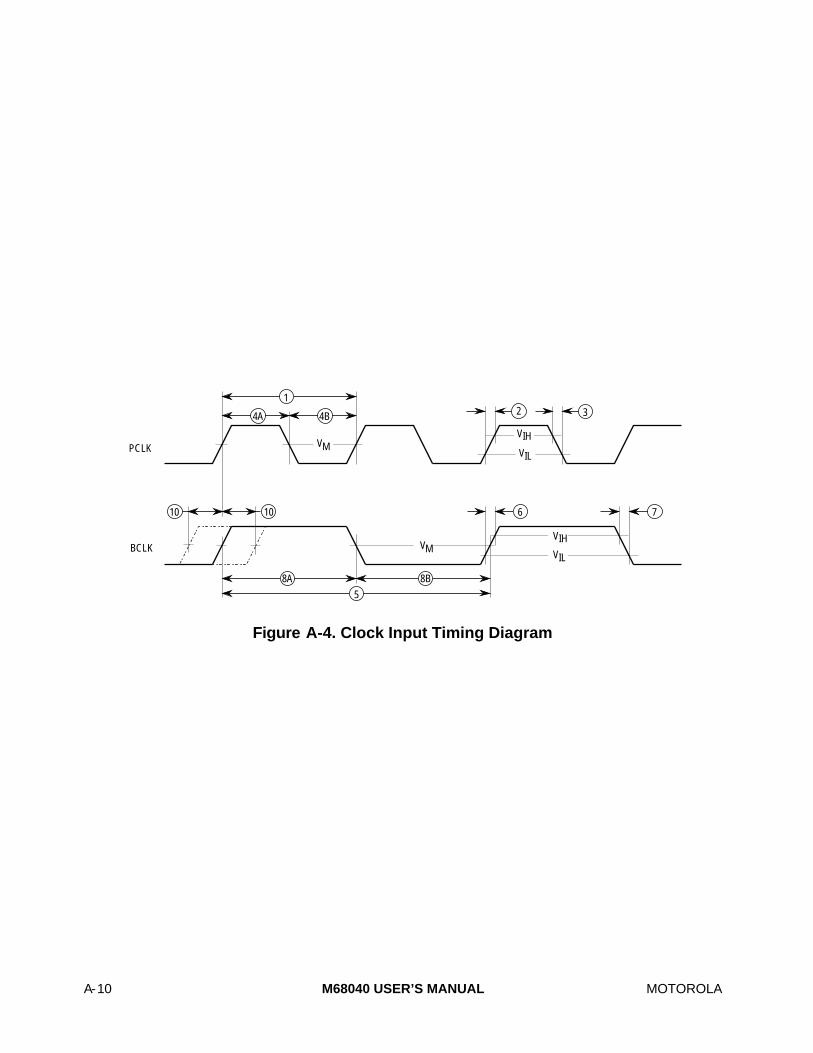
A-10 M68040 USER’S MANUAL MOTOROLA
2 31
5
6 71010
PCLK
BCLK
8B8A
4A 4B
VMV
V
IH
IL
VIH
VILVM
Figure A-4. Clock Input Timing Diagram

MOTOROLA M68040 USER’S MANUAL A-11
A.6.6 Output AC Timing Specifications (see Figures A-5* to A-9)
20 MHz 25 MHz 33 MHz
Num Characteristic Min Max Min Max Min Max Unit
11 BCLK to Address, CIOUT , LOCK, LOCKE , PSTx, R/W, SIZx, TLNx ,TMx, TTx, UPAxValid
11.5 35 9 30 6.5 25 ns
12 BCLK to Output Invalid (Output Hold) 11.5 — 9 — 6.5 — ns
13 BCLK to TS Valid 11.5 35 9 30 6.5 25 ns
14 BCLK to TIP Valid 11.5 35 9 30 6.5 25 ns
18 BCLK to Data-Out Valid 11.5 37 9 32 6.5 27 ns
19 BCLK to Data-Out Invalid (Output Hold) 11.5 — 9 — 6.5 — ns
20 BCLK to Output Low Impedance 11.5 — 9 — 6.5 — ns
21 BCLK to Data-Out High Impedance 11.5 25 9 20 6.5 17 ns
38 BCLK to Address, CIOUT , LOCK, LOCKE ,R/W, SIZx, TS, TLNx, TMx, TTx, UPAx HighImpedance
11.5 23 9 18 6.5 15 ns
39 BCLK to BB, TA, TIP High Impedance 23 33 19 28 14 25 ns
40 BCLK to BR , BB Valid 11.5 35 9 30 6.5 23 ns
43 BCLK to MI Valid 11.5 35 9 30 6.5 25 ns
48 BCLK to TA Valid 11.5 35 9 30 6.5 25 ns
50 BCLK to IPEND, PSTx, RSTO Valid 11.5 35 9 30 6.5 25 ns
* Output timing is specified for a valid signal measured at the pin. Timing is specified driving an unterminated 30-Ωtransmission line with a length characterized by a 2.5-ns one-way propagation delay. Buffer output impedance istypically 30 Ω; the buffer specifications include approximately 5 ns for the signal to propagate the length of thetransmission line and back.
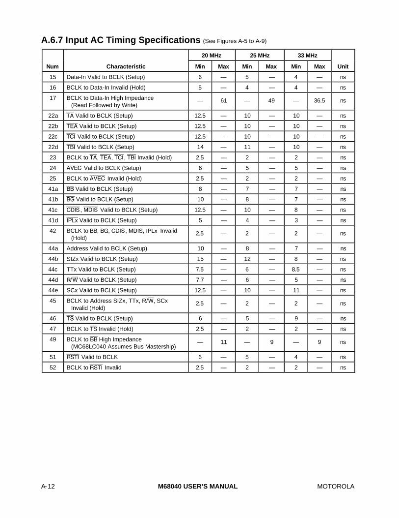
A-12 M68040 USER’S MANUAL MOTOROLA
A.6.7 Input AC Timing Specifications (See Figures A-5 to A-9)
20 MHz 25 MHz 33 MHz
Num Characteristic Min Max Min Max Min Max Unit
15 Data-In Valid to BCLK (Setup) 6 — 5 — 4 — ns
16 BCLK to Data-In Invalid (Hold) 5 — 4 — 4 — ns
17 BCLK to Data-In High Impedance(Read Followed by Write)
— 61 — 49 — 36.5 ns
22a TA Valid to BCLK (Setup) 12.5 — 10 — 10 — ns
22b TEA Valid to BCLK (Setup) 12.5 — 10 — 10 — ns
22c TCI Valid to BCLK (Setup) 12.5 — 10 — 10 — ns
22d TBI Valid to BCLK (Setup) 14 — 11 — 10 — ns
23 BCLK to TA, TEA, TCI , TBI Invalid (Hold) 2.5 — 2 — 2 — ns
24 AVEC Valid to BCLK (Setup) 6 — 5 — 5 — ns
25 BCLK to AVEC Invalid (Hold) 2.5 — 2 — 2 — ns
41a BB Valid to BCLK (Setup) 8 — 7 — 7 — ns
41b BG Valid to BCLK (Setup) 10 — 8 — 7 — ns
41c CDIS , MDIS Valid to BCLK (Setup) 12.5 — 10 — 8 — ns
41d IPL≈ Valid to BCLK (Setup) 5 — 4 — 3 — ns
42 BCLK to BB, BG, CDIS , MDIS, IPL≈ Invalid (Hold)
2.5 — 2 — 2 — ns
44a Address Valid to BCLK (Setup) 10 — 8 — 7 — ns
44b SIZx Valid to BCLK (Setup) 15 — 12 — 8 — ns
44c TTx Valid to BCLK (Setup) 7.5 — 6 — 8.5 — ns
44d R/W Valid to BCLK (Setup) 7.7 — 6 — 5 — ns
44e SCx Valid to BCLK (Setup) 12.5 — 10 — 11 — ns
45 BCLK to Address SIZx, TTx, R/W, SCxInvalid (Hold)
2.5 — 2 — 2 — ns
46 TS Valid to BCLK (Setup) 6 — 5 — 9 — ns
47 BCLK to TS Invalid (Hold) 2.5 — 2 — 2 — ns
49 BCLK to BB High Impedance(MC68LC040 Assumes Bus Mastership)
— 11 — 9 — 9 ns
51 RSTI Valid to BCLK 6 — 5 — 4 — ns
52 BCLK to RSTI Invalid 2.5 — 2 — 2 — ns

MOTOROLA M68040 USER’S MANUAL A-13
2223
11
BCLK
A31–A0
TRANSFER ATTRIBUTES
D31–D0 IN (READ)
12
1516
D31–D0 OUT (WRITE)
1921
13 12
14
18
20
TA
TEA
TCI
TBI
TIP
TS
NOTE: Transfer Attribute Signals = UPAx, SIZx, TTx, TMx, TLNx, R/W, LOCK, LOCKE, CIOUT
AVEC
2425
12
Figure A-5. Read/Write Timing

A-14 M68040 USER’S MANUAL MOTOROLA
BCLK
A31–A0
TRANSFER ATTRIBUTES
38
20
11
TS
TIP
BB OUT12
39
BG
BR
41 42
12
21
D31–D0 OUT (WRITE)
20
40
13
14
MI
4312
1239
40
NOTE: Transfer Attribute Signals = UPAx, SIZx, TTx, TMx, TLNx, R/W, CIOUT
LOCK, LOCKE
Figure A-6. Bus Arbitration Timing
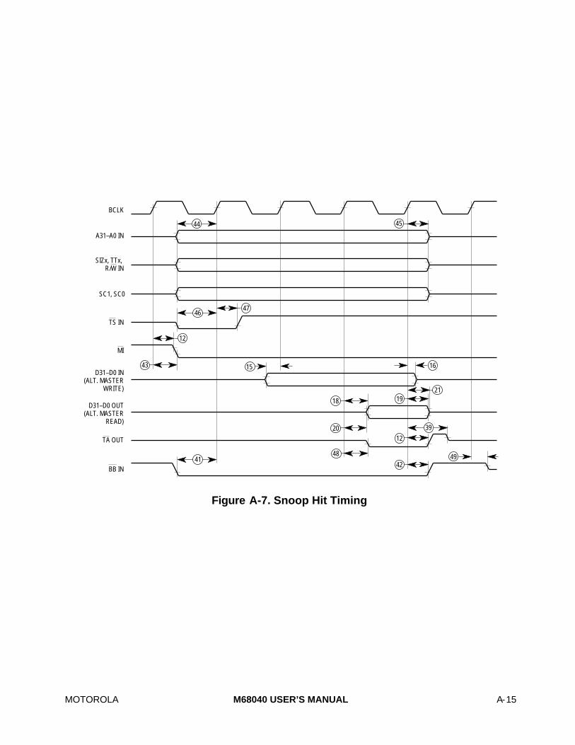
MOTOROLA M68040 USER’S MANUAL A-15
D31–D0 IN (ALT. MASTER
WRITE)
D31–D0 OUT (ALT. MASTER
READ)
44
BCLK
A31–A0 IN
15 16
4647
12
4148
1220 39
4249
43
1921
18
TS IN
MI
TA OUT
BB IN
SIZx, TTx, R/W IN
45
SC1, SC0
Figure A-7. Snoop Hit Timing

A-16 M68040 USER’S MANUAL MOTOROLA
TBI
TS IN
MI
SIZx, TTx, R/W IN
44
BCLK
A31–A0 IN
TEA
47
SC1, SC0 SNOOP
43
TA
45
2223
BB IN41
42
43
12
46
Figure A-8. Snoop Miss Timing
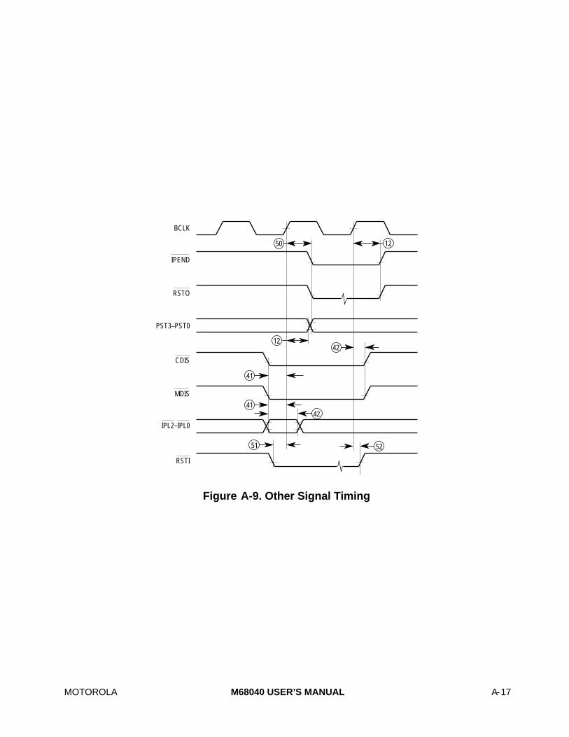
MOTOROLA M68040 USER’S MANUAL A-17
50
BCLK
12
42
41
IPEND
RSTO
CDIS
MDIS
IPL2–IPL0
42
PST3–PST0
12
RSTI
51 52
41
Figure A-9. Other Signal Timing

A-18 M68040 USER’S MANUAL MOTOROLA

MOTOROLA M68040 USER’S MANUAL B-1
APPENDIX BMC68EC040
NOTE
All references to MC68EC040 also apply to the MC68EC040V.Refer to Appendix C MC68040V and MC68EC040V for moreinformation on the MC68EC040V.
The MC68EC040 is Motorola's third generation of M68000-compatible, high-performance,32-bit microprocessors. The MC68EC040 is an embedded controller employing a highlyintegrated architecture to provide very high performance in a monolithic HCMOS device.The MC68EC040 integrates an MC68040-compatible integer unit, an access control unit(ACU), and independent 4-Kbyte instruction and data caches. A six-stage instructionpipeline, multiple internal buses, and a full internal Harvard architecture, includingseparate caches for both instruction and data accesses, provides a high degree ofinstruction execution parallelism. The inclusion of on-chip bus snooping logic, whichdirectly supports cache coherency in multimaster applications, enhances cachefunctionality.
The MC68EC040 is user-object-code compatible with previous members of the M68000family and is specifically optimized to reduce the execution time of compiler-generatedcode. The MC68EC040 is pin compatible with the MC68040 and MC68LC040. TheMC68EC040 is implemented in Motorola’s latest HCMOS technology, providing an idealbalance between speed, power, and physical device size. Figure B-1 provides a simplifiedblock diagram of the MC68EC040.
The main features of the MC68EC040 include:
• MC68040-Compatible Integer Execution Unit
• 4-Kbyte Instruction Cache and 4-Kbyte Data Cache Accessible Simultaneously
• 32-Bit, Nonmultiplexed External Address and Data Buses with Synchronous BurstingInterface
• User-Object-Code Compatible with All M68000 Microprocessors
• Concurrent Integer Unit, ACU, and Bus Controller Operation Maximizes Throughput
• Low-Latency Bus Accesses for Reduced Cache-Miss Penalty
• Multimaster/Multiprocessor Support via Bus Snooping
• 4-Gbyte Direct Addressing Range
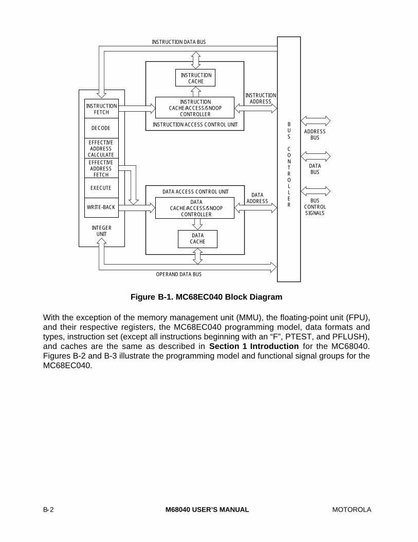
B-2 M68040 USER’S MANUAL MOTOROLA
INSTRUCTION FETCH
DECODE
EFFECTIVE ADDRESS
CALCULATE
EXECUTE
EFFECTIVE ADDRESS
FETCH
INSTRUCTION CACHE/ACCESS/SNOOP
CONTROLLER
BUS CONTROL SIGNALS
DATA BUS
ADDRESS BUS
DATA CACHE/ACCESS/SNOOP
CONTROLLER
OPERAND DATA BUS
INSTRUCTION DATA BUS
INSTRUCTION CACHE
DATA CACHE
DATA ACCESS CONTROL UNIT
INSTRUCTION ACCESS CONTROL UNIT B U S
C O N T R O L L E R
INSTRUCTION ADDRESS
DATA ADDRESS
WRITE-BACK
INTEGER UNIT
Figure B-1. MC68EC040 Block Diagram
With the exception of the memory management unit (MMU), the floating-point unit (FPU),and their respective registers, the MC68EC040 programming model, data formats andtypes, instruction set (except all instructions beginning with an “F”, PTEST, and PFLUSH),and caches are the same as described in Section 1 Introduction for the MC68040.Figures B-2 and B-3 illustrate the programming model and functional signal groups for theMC68EC040.

MOTOROLA M68040 USER’S MANUAL B-3
SUPERVISOR PROGRAMMING MODEL
USER PROGRAMMING MODEL
CCRPC A7/USPA6A5A4A3A2A1A0
D7D6D5D4D3D2D1D0
31 0
DATA REGISTERS
ADDRESS REGISTERS
31 0
A7'/ISPA7"/MSPSRVBRSFC DFCCACRDACR0DACR1IACR0IACR1
(CCR)
PROGRAM COUNTERCONDITION CODE REGISTER
INTERRUPT STACK POINTERMASTER STACK POINTERSTATUS REGISTERVECTOR BASE REGISTERSOURCE FUNCTION CODEDESTINATION FUNCTION CODECACHE CONTROL REGISTERDATA ACCESS CONTROL REGISTER 0DATA ACCESS CONTROL REGISTER 1INSTRUCTION ACCESS CONTROL REGISTER 0INSTRUCTION ACCESS CONTROL REGISTER 1
USER STACK POINTER
Figure B-2. MC68EC040 Programming Model

B-4 M68040 USER’S MANUAL MOTOROLA
MC68EC040
VCC
GND
BUS ARBITRATIONBGBR
BB
BUS SNOOP CONTROL AND RESPONSE
M I
INTERRUPT CONTROL
IPL0
AVEC
IPEND
PROCESSOR CONTROL
CDIS
RSTIRSTO
PCLKBCLK
TESTTRST
TMSTCK
TDI
POWER SUPPLY
TDO
SC0SC1
IPL1IPL2
STATUS AND CLOCKS
PST0PST1PST2
DATA BUS D31–D0
TRANSFER ATTRIBUTES
MASTER TRANSFER CONTROL
A31–A0ADDRESS BUS
TS
TIP
TCISLAVE
TRANSFER CONTROL
TEA
TBI
R/W
LOCKECIOUT
TT0TT1TM0TM1TM2
TLN0TLN1UPA0UPA1
SIZ0SIZ1
LOCK
TA
PST3
JS0JS1
Figure B-3. MC68EC040 Functional Signal Groups
B.1 MC68EC040 DIFFERENCES
The following differences exist between the MC68EC040 and MC68040:
• Two independent access control units (ACUs) replace the MC68040 MMUs. TheACU has four corresponding registers (access control registers) that the MC68040implements as data transparent translation registers. The page size is fixed at4 Kbytes.
• PTEST and PFLUSH instructions cause an indeterminate result (i.e., anundetermined number of bus cycles); the user should not execute them on theMC68EC040.
• The MC68EC040 does not contain an FPU, which causes unimplemented floating-point exceptions to occur using a new stack frame format.
MOTOROLA M68040 USER’S MANUAL B-5
• The DLE and MDIS pin names have been changed to JS0 and JS1, respectively.
• The MC68EC040 does not implement the DLE mode, multiplexed, or output bufferimpedance selection modes of operation. The MC68EC040 implements only thesmall output buffer mode of operation. All timing and drive capabilities of theMC68EC040 are equivalent to those of the MC68040 in the small buffer mode ofoperation.
B.2 JTAG SCAN (JS1–JS0)
The MC68040 MDIS and DLE pin names have been changed to JS1 and JS0respectively. During normal operation, the JS1 and JS0 pin cannot float, they must be tiedto GND or Vcc directly or through a resistor. During board testing, these pins retain thefunctionality of the JTAG scan of the MC68040 for compatibility purposes. Refer toSection 6 IEEE 1149.1 Test Access Port (JTAG) for details concerning IEEE 1149.1Standard Test Access Port and Boundary Scan Architecture.
B.3 ACCESS CONTROL UNITS
The information in this section replaces the information in Section 3 MemoryManagement Unit (Except MC68EC040 and MC68EC040V). When reading Section 4Instruction and Data Caches, disregard any references to the MMU; remember thefunctionality of the access control registers has replaced that of transparent translationregisters. The MC68EC040 contains two independent ACUs, one for instructions and onefor data. Each ACU allows memory selections to be made requiring attributes particular toperipherals, shared memory, or other special memory requirements. The followingparagraphs describe the ACUs and the access control registers contained in them.
B.3.1 Access Control Registers
Each ACU has two independent access control registers (ACRs). The instruction ACUcontains the instruction access control registers (IACR0 and IACR1). The data ACUcontains the data access control registers (DACR0 and DACR1). Both ACRs provide andcontrol status information for access control of memory in the MC68EC040. Onlyprograms that execute in the supervisor mode using the MOVEC instruction can directlyaccess the ACRs.
The 32-bit ACRs each define blocks of address space for access control. These blocks ofaddress space can overlap or be separate, and are a minimum of 16 Mbytes. Threeblocks are used with two user-defined attributes, cachability control and optional writeprotection. The ACRs specify a block of address space as serialized noncachable forperipheral selections and as write-through for shared blocks of address space in multi-processing applications. The ACRs can be configured to support many embedded controlapplications while maintaining cache integrity. Refer to Section 4 Instruction and DataCaches for details concerning cachability. Figure B-4 illustrates the ACR format.

B-6 M68040 USER’S MANUAL MOTOROLA
31 24 23 16 15 14 13 12 11 10 9 8 7 6 5 4 3 2 1 0
LOGICAL ADDRESS BASE LOGICAL ADDRESS MASK E S 0 0 0 U1 U0 0 CM 0 0 W 0 0
Figure B-4. MC68EC040 Access Control Register Format
ADDRESS BASEThis 8-bit field is compared with physical address bits A31–A24. Addresses that matchin this comparison (and are otherwise eligible) are accessible.
ADDRESS MASKThis 8-bit field contains a mask for the ADDRESS BASE field. Setting a bit in theADDRESS MASK field causes the processor to ignore the corresponding bit in theADDRESS BASE field. Setting some of the ADDRESS MASK bits to ones obtainsblocks of memory larger than 16 Mbytes. The low-order bits of this field are normally setto define contiguous blocks larger than 16 Mbytes, although contiguous blocks are notrequired.
E—EnableThis bit enables and disables transparent translation of the block defined by thisregister. Refer to Section 3 Memory Management Unit (Except MC68EC040 andMC68EC040V) for details on transparent translation.
0 = Access control disabled.1 = Access control enabled.
S—Supervisor/User ModeThis field specifies the way FC2 is used in matching an address:
00 = Match only if FC2 = 0 (user mode access).01 = Match only if FC2 = 1 (supervisor mode access).
10, 11 = Ignore FC2 when matching.
U1, U0—User Page AttributesThese two bits drive on the user page attribute signals (UPA1 and UPA0). If an externalbus transfer results from the access, U0 and U1 are echoed to the UPA0 and UPA1signals, respectively. The user can program these bits to support extended addressing,bus snooping, or other applications. The MC68EC040 does not interpret these bits.
CM—Cache ModeThis field selects the cache mode and access serialization for a page as follows:
00 = Cachable, Write-through01 = Cachable, Copyback10 = Noncachable, Serialized11 = Noncachable
Detailed information on caching modes is available in Section 4 Instruction and DataCaches, and information on serialization is available in Section 7 Bus Operation.

MOTOROLA M68040 USER’S MANUAL B-7
W—Write ProtectThis bit indicates if the transparent block is write protected. If set, write and read-modify-write accesses are aborted as if the R-bit in a table descriptor were clear. Refer to 3.2.2Descriptors for a description of table descriptors.
0 = Read and write accesses permitted.1 = Write accesses not permitted.
B.3.2 Address Comparison
The following description of address comparison assumes that the ACRs are enabled.Clearing the E-bit in each ACR independently disables access control, causing theprocessor to ignore it.
When an ACU receives a physical address, the privilege mode and the eight high-orderbits of the address are compared to the block of addresses defined by the two ACRs forthe corresponding ACU. Each block of address space for an ACR contains an S-field, aBASE ADDRESS field, and an ADDRESS MASK field. The S-field allows for matchingeither user or supervisor accesses (or both). Setting a bit in the ADDRESS MASK fieldcauses the corresponding bit of the ADDRESS BASE to be ignored in the addresscomparison and privilege mode. Setting successively higher order bits in the ADDRESSMASK field increases the size of the block of address space.
The address for the current bus cycle and an ACR address match when the privilegemode and address bits for each (not including the masked bits) are equal. Each ACRspecifies write protection for the block of address space. Enabling write protection for ablock of address space causes the abortion of write or read-modify-write accesses to theblock, and an access error exception occurs.
By appropriately configuring an ACR, flexible mappings can be specified. For example, tocontrol access to the user address space, the S-field equals $0, and the ADDRESS MASKfield equals $FF in all four ACRs. To control access to the supervisor address space($00000000–$0FFFFFFF) with write protection, the BASE ADDRESS field = $0X, theADDRESS MASK field equals $0F, the W-bit is set to one, and the S-field = $1. Theinclusion of independent ACRs in both the instruction ACU (IACU) and data ACU (DACUprovides an exception to the merged instruction and data address space, allowingdifferent access control for instruction and operand accesses. Also, since the instructionmemory unit is only used for instruction prefetches, different instruction and data ACRscan cause PC relative operand fetches to be translated differently from instructionprefetches.
Matching either of the ACRs in a corresponding ACU during an access to a memory unitcompletes the access with the ACU. If both registers match, the access uses the xACR0status bits. Addresses are passed through without translation if there is no match in theACRs and no table search occurs. The MC68EC040 does not perform table searches.

B-8 M68040 USER’S MANUAL MOTOROLA
B.3.3 Effect of RSTI on the ACU
When the assertion of the reset input (RSTI) signal resets the MC68EC040, the E-bits ofthe ACRs are cleared, disabling address access control.
B.4 SPECIAL MODES OF OPERATION
This part of the M68040 User's Manual does not apply to the MC68EC040. TheMC68EC040 does not sample the IPL2–IPL0, CDIS, JS0 (DLE on the MC68040), or JS1(MDIS on the MC68040) pins on the rising edge of RSTI.
An external device asserts RSTI to reset the processor. When power is applied to thesystem, external circuitry should assert RSTI for a minimum of 10 BCLK cycles after VCCis within tolerance. Figure B-5 is a functional timing diagram of the power-on resetoperation, illustrating the relationships between VCC, RSTI, and bus signals. The BCLKand PCLK clock signals are required to be stable by the time VCC reaches the minimumoperating specification. RSTI is internally synchronized for two BCLKS before being used,and must meet the specified setup and hold times to BCLK (specifications #51 and #52 inB.7 MC68EC040 Electrical Characteristics) only if recognition by a specific BCLK risingedge is required.
BCLK
+5V
0V
RSTI
TS
BR
BG
BB
TIP
VCC
Undefined
t 10 CLOCKS
2 CLOCKS
128 CLOCKS
>
MI
Figure B-5. MC68EC040 Initial Power-On Reset Timing

MOTOROLA M68040 USER’S MANUAL B-9
Once RSTI is negated, the processor is internally held in reset for another 128 clockcycles. During the reset period, all three-statable signals are three-stated, and the rest aredriven to their inactive state. Once the internal reset signal negates, all bus signals remainin a high-impedance state until the processor is granted the bus. After this, the first buscycle for reset exception processing begins. In Figure B-6, the processor assumes implicitownership of the bus before the first bus cycle begins. The levels on the CDIS, JS1 (MDIS
on the MC68040), and IPL2–IPL0 signals are not sampled when RSTI is negated.
For processor resets after the initial power-on reset, RSTI should be asserted for at least10 clock periods. Figure B-6 illustrates timing associated with a reset when the processoris executing bus cycles. Note that BB and TIP (and TA driven during a snooped access)are asserted before transitioning to a three-state level. Processor reset causes any buscycle in progress to terminate as if TA or TEA had been asserted. Also, the processorinitializes registers appropriately for a reset exception.
BCLK
BUS SIGNALS
RSTI
TS
BR
BG
BB
TIP
t 10 CLOCKS
2 CLOCKS
128 CLOCKS
>
MI
Figure B-6. MC68EC040 Normal Reset Timing
When a RESET instruction is executed, the processor drives the reset out (RSTO) signalfor 512 BCLK cycles. In this case, the processor resets the external devices of the system,and the internal registers of the processor are unaffected. The external devices connectedto RSTO are reset at the completion of the RESET instruction. An RSTI signal that isasserted to the processor during execution of a RESET instruction immediately resets theprocessor and causes RSTO to negate. RTSO can be logically ANDed with the externalsignal driving RTSI to derive a system reset signal that is asserted for both an externalprocessor reset and execution of a RESET instruction.

B-10 M68040 USER’S MANUAL MOTOROLA
B.5 EXCEPTION PROCESSING
The MC68EC040 provides five different stack frames for exception processing and allowsfor a MC68040-specific stack frame. Refer to Section 8 Exception Processing for detailson exception processing.
B.5.1 Unimplemented Floating-Point Instructions and Exceptions
All legal MC68040 and MC68881/MC68882 floating-point instructions are defined asunimplemented floating-point instructions on the MC68EC040. These instructionsgenerate an eight-word stack frame (format $4) during exception processing before takingan F-line exception. These instructions trap as an F-line exception and can be emulated insoftware by the F-line exception handler to maintain user-object-code compatibility.
The MC68EC040 assists the emulation process by distinguishing unimplemented floating-point instructions from other unimplemented F-line instructions. To aid emulation, theeffective address is calculated and saved in the format $4 stack frame. This simplifies andspeeds up the emulation process by eliminating the need for the emulation routine todetermine the effective address and by providing information required to emulate theinstruction on the exception stack frame in the supervisor address space. However, thefloating-point instruction can reside in user space; therefore, the floating-pointunimplemented exception handler may need to access user instruction space. Thefollowing processing steps occur for an unimplemented floating-point instruction:
1. When an unimplemented floating-point instructionis encountered, the instruction ispartially decoded, and the effective address is calculated, if required.
2. The processor waits for all previous integer instructions, write-backs, and associatedexception processing to complete before beginning exception processing for theunimplemented floating-point instruction. Any access error that occurs in completingthe write-backs causes an access error exception, and the resulting stack frameindicates a pending unimplemented floating-point instruction exception. The accesserror exception handler then completes the write-backs in software, and exceptionprocessing for the unimplemented floating-point instruction exception beginsimmediately after return from the access error handler.
3. The processor begins exception processing for the unimplemented floating-pointinstruction by making an internal copy of the current SR. The processor then entersthe supervisor mode and clears the trace bits (T1 and T0). It creates a format $4stack frame and saves the internal copy of the SR, PC, vector offset, calculatedeffective address, and PC value of the faulted instruction in the stack frame.
The effective address field of the format $4 stack frame contains the calculatedeffective address of the operand for the faulted floating-point instruction using theaddressing mode in which the effective address is calculated. For immediate andregister direct addressing modes, this field is $0. The saved PC value is the logicaladdress of the instruction that follows the unimplemented floating-point instruction.This value will be restored during RTE execution. The vector offset format number($4) is used for this eight-word stack frame. Note that an MC68040 cannot correctlyhandle a stack format $4. The PC of the faulted instruction contains a long-word PCof the floating-point instruction that caused the trap to occur. The information isprovided so that the instruction is available for software emulation of floating-point

MOTOROLA M68040 USER’S MANUAL B-11
instructions. The processor generates exception vector number 11 for theunimplemented F-line instruction exception vector, fetches the address of the F-lineexception handler from the exception vector table, and begins execution of thehandler after prefetching instructions to fill the pipeline. Refer to Section 8Exception Processing for details about exception processing.
B.5.2 MC68EC040 Stack Frames
When the processor executes an RTE instruction, it examines the stack frame on top ofthe active supervisor stack to determine if it is a valid frame and what type of contextrestoration it requires. The set of stack frames included for exception processing are four-and six-word stack frames, a four-word throwaway stack frame, an access error stackframe, and a new eight-word unimplemented floating-point stack frame. The stack framethat the MC68040 can generate and the MC68EC040 can process is the floating-pointpost-instruction stack frame. Refer to Section 8 Exception Processing for details aboutexception stack frames.
Eight-Word Stack Frame (Format $4)
Stack Frames Exception Types Stacked PC Points To
SP STATUS REGISTERPROGRAM COUNTER
VECTOR OFFSET0100+$02
+$06
+$08
+$0C
15 0
EFFECTIVE ADDRESS
PC OF FAULTED INSTRUCTION
• The MC68040 cannotgenerate or read this stack.
• Effective address field isthe address of the faultedinstruction operand.
When the MC68EC040 writes or reads a stack frame, it uses long-word operand transferswherever possible. Using a long-word-aligned stack pointer greatly enhances exceptionprocessing performance. The processor does not necessarily read or write the stackframe data in sequential order. The system software should not depend on a particularexception generating a particular stack frame. For compatibility with future devices, thesoftware should be able to handle any type of stack frame for any type of exception. TheMC68EC040 does not generate the floating-point post-instruction stack frame. TheMC68040 cannot accept the eight-word unimplemented stack frame. The MC68EC040can handle all MC68040 stack frame formats.

B-12 M68040 USER’S MANUAL MOTOROLA
This device contains protectivecircuitry against damage due to highstatic voltages or electrical fields;however, it is advised that normalprecautions be taken to avoidapplication of any voltages higherthan maximum-rated voltages to thishigh-impedance circuit. Reliablity ofoperation is enhanced if unusedinputs are tied to an appropriatelogic voltage level (e.g., either GNDor VCC).
B.6 SOFTWARE CONSIDERATIONS
The following MC68EC040 instructions are different from the MC68040: PTEST, PFLUSH,CPUSH, CINV, MOVEC, and all floating-point instructions.
The PTEST and PFLUSH instructions should not be executed. Execution of the PTESTinstruction causes random bus cycles to occur. Execution of the PFLUSH instructionproduces indeterminate results. Neither instruction causes the MC68EC040 to generatean exception.
The CPUSH and CINV instructions require special consideration. A page is defined as a4-Kbyte block of external memory. The CPUSH and CINV page instruction opcodes canbe used to push or invalidate 4-Kbyte blocks of memory. The MC68EC040 does notsupport 8-Kbyte pages.
The MOVEC to URP and SRP instructions are not valid and will produce indeterminateresults. Each ACU has a status register and translation control register that replace theMMU status register and translation control register of the MC68040. The MMU statusregister opcode of the MOVEC instruction can modify the ACU status register. TheMC68EC040 ACU status register does not provide additional functionality to the ACU andis only provided for compatibility with the ACU MC68EC030 status register. The ACUstatus register may not be implemented in future M68EC0X0 products.
B.7 MC68EC040 ELECTRICAL CHARACTERISTICS
The following paragraphs provide information on the maximum rating and thermalcharacteristics for the MC68EC040 only. Refer to Appendix C MC68040V andMC68EC040V for more information on electrical characteristics for the MC68EC040V.This section is subject to change. For the most recent specifications, contact a Motorolasales office or complete the registration card at the end of this manual.
B.7.1 Maximum Ratings
Characteristic Symbol Value Unit
Supply Voltage VCC –0.3 to +7.0 V
Input Voltage Vin –0.8 to +7.0 V
Maximum Operating Junction Temperature TJ 110 °C
Minimum Operating Ambient Temperature TA 0 °C
Storage Temperature Range Tstg –55 to 150 °C
B.7.2 Thermal Characteristics
Characteristic Symbol Value Rating
Thermal Resistance, Junction to Case—PGA Package
θJC 3 °C/W
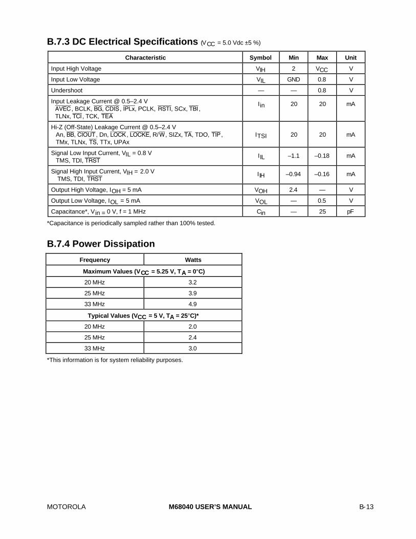
MOTOROLA M68040 USER’S MANUAL B-13
B.7.3 DC Electrical Specifications (VCC = 5.0 Vdc ±5 %)
Characteristic Symbol Min Max Unit
Input High Voltage VIH 2 VCC V
Input Low Voltage VIL GND 0.8 V
Undershoot — — 0.8 V
Input Leakage Current @ 0.5–2.4 VAVEC , BCLK, BG, CDIS , IPL≈, PCLK, RSTI, SCx, TBI ,TLNx, TCI , TCK, TEA
Iin 20 20 mA
Hi-Z (Off-State) Leakage Current @ 0.5–2.4 VAn, BB, CIOUT , Dn, LOCK , LOCKE, R/W , SIZx, TA, TDO, TIP ,TMx, TLNx, TS, TTx, UPAx
ITSI 20 20 mA
Signal Low Input Current, VIL = 0.8 VTMS, TDI, TRST
IIL –1.1 –0.18 mA
Signal High Input Current, VIH = 2.0 V TMS, TDI, TRST
IIH –0.94 –0.16 mA
Output High Voltage, IOH = 5 mA VOH 2.4 — V
Output Low Voltage, IOL = 5 mA VOL — 0.5 V
Capacitance*, Vin = 0 V, f = 1 MHz Cin — 25 pF
*Capacitance is periodically sampled rather than 100% tested.
B.7.4 Power Dissipation
Frequency Watts
Maximum Values (VCC = 5.25 V, TA = 0°C)
20 MHz 3.2
25 MHz 3.9
33 MHz 4.9
Typical Values (VCC = 5 V, TA = 25°C)*
20 MHz 2.0
25 MHz 2.4
33 MHz 3.0
*This information is for system reliability purposes.

B-14 M68040 USER’S MANUAL MOTOROLA
B.7.5 Clock AC Timing Specifications (see Figure B-7)
20 MHz 25 MHz 33 MHz
Num Characteristic Min Max Min Max Min Max Unit
Frequency of Operation 16.67 20 16.67 25 16.67 33.3 MHz
1 PCLK Cycle Time 25 30 20 30 15 30 ns
2 PCLK Rise Time — 1.7 — 1.7 — 1.7 ns
3 PCLK Fall Time — 1.6 — 1.6 — 1.6 ns
4 PCLK Duty Cycle Measured at 1.5 V 48 52 47.5 52.5 46.67 53.33 %
4a* PCLK Pulse Width High Measured at 1.5 V 12 13 9.5 10.5 7 8 ns
4b* PCLK Pulse Width Low Measured at 1.5 V 12 13 9.5 10.5 7 8 ns
5 BCLK Cycle Time 50 60 40 60 30 60 ns
6,7 BCLK Rise and Fall Time — 4 — 4 — 3 ns
8 BCLK Duty Cycle Measured at 1.5 V 40 60 40 60 40 60 %
8a* BCLK Pulse Width High Measured at 1.5 V 20 30 16 24 12 18 ns
8b* BCLK Pulse Width Low Measured at 1.5 V 20 30 16 24 12 18 ns
9 PCLK, BCLK Frequency Stability — 1000 — 1000 — 1000 ppm
10 PCLK to BCLK Skew — 9 — 9 — n/a ns
*Specification value at maximum frequency of operation.
2 31
5
6 71010
PCLK
BCLK
8B8A
4A 4B
VMV
V
IH
IL
VIH
VILVM
Figure B-7. Clock Input Timing Diagram

MOTOROLA M68040 USER’S MANUAL B-15
B.7.6 Output AC Timing Specifications (see Figures B-8* to B-12)
20 MHz 25 MHz 33 MHz
Num Characteristic Min Max Min Max Min Max Unit
11 BCLK to Address CIOUT, LOCK , LOCKE,R/W, SIZx, TLNx ,TMx, TTx, UPAx Valid
11.5 35 9 30 6.5 25 ns
12 BCLK to Output Invalid (Output Hold) 11.5 — 9 — 6.5 — ns
13 BCLK to TS Valid 11.5 35 9 30 6.5 25 ns
14 BCLK to TIP Valid 11.5 35 9 30 6.5 25 ns
18 BCLK to Data-Out Valid 11.5 37 9 32 6.5 27 ns
19 BCLK to Data-Out Invalid (Output Hold) 11.5 — 9 — 6.5 — ns
20 BCLK to Output Low Impedance 11.5 — 9 — 6.5 — ns
21 BCLK to Data-Out High Impedance 11.5 25 9 20 6.5 17 ns
38BCLK to Address, CIOUT , LOCK, LOCKE ,
R/W, SIZx, TS, TLNx, TMx, TTx, UPAx HighImpedance
11.5 23 9 18 6.5 15 ns
39 BCLK to BB, TA, TIP High Impedance 23 33 19 28 14 25 ns
40 BCLK to BR , BB Valid 11.5 35 9 30 6.5 23 ns
43 BCLK to MI Valid 11.5 35 9 30 6.5 25 ns
48 BCLK to TA Valid 11.5 35 9 30 6.5 25 ns
50 BCLK to IPEND, PSTx, RSTO Valid 11.5 35 9 30 6.5 25 ns
* Output timing is specified for a valid signal measured at the pin. Timing is specified driving an unterminated 30-Ωtransmission line with a length characterized by a 2.5-ns one-way propagation delay. Buffer output impedance istypically 30 Ω; the buffer specifications include approximately 5 ns for the signal to propagate the length of thetransmission line and back.
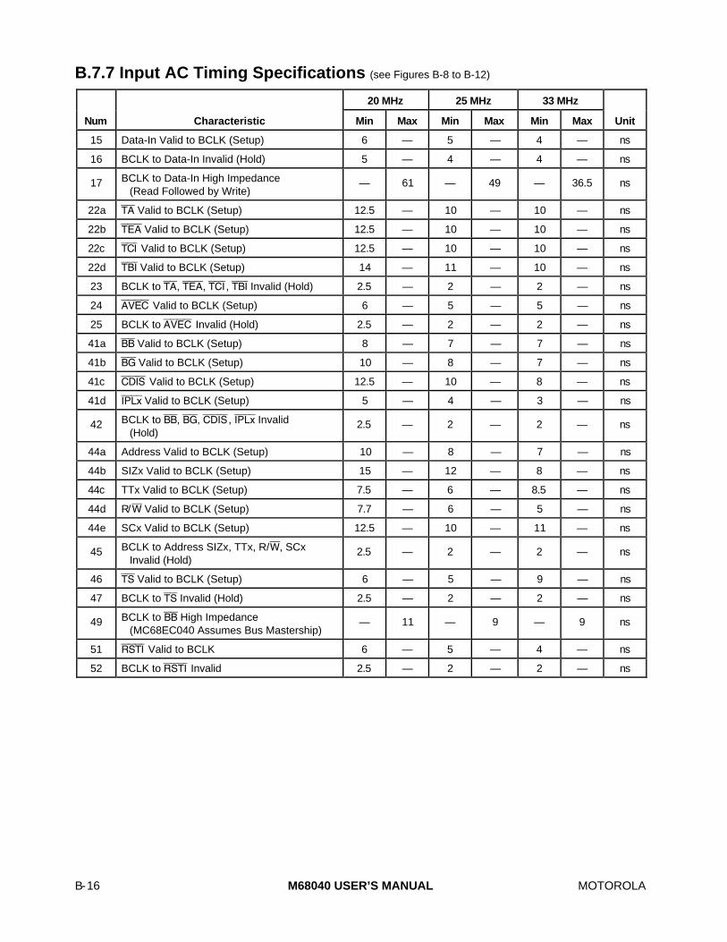
B-16 M68040 USER’S MANUAL MOTOROLA
B.7.7 Input AC Timing Specifications (see Figures B-8 to B-12)
20 MHz 25 MHz 33 MHz
Num Characteristic Min Max Min Max Min Max Unit
15 Data-In Valid to BCLK (Setup) 6 — 5 — 4 — ns
16 BCLK to Data-In Invalid (Hold) 5 — 4 — 4 — ns
17 BCLK to Data-In High Impedance(Read Followed by Write)
— 61 — 49 — 36.5 ns
22a TA Valid to BCLK (Setup) 12.5 — 10 — 10 — ns
22b TEA Valid to BCLK (Setup) 12.5 — 10 — 10 — ns
22c TCI Valid to BCLK (Setup) 12.5 — 10 — 10 — ns
22d TBI Valid to BCLK (Setup) 14 — 11 — 10 — ns
23 BCLK to TA, TEA, TCI , TBI Invalid (Hold) 2.5 — 2 — 2 — ns
24 AVEC Valid to BCLK (Setup) 6 — 5 — 5 — ns
25 BCLK to AVEC Invalid (Hold) 2.5 — 2 — 2 — ns
41a BB Valid to BCLK (Setup) 8 — 7 — 7 — ns
41b BG Valid to BCLK (Setup) 10 — 8 — 7 — ns
41c CDIS Valid to BCLK (Setup) 12.5 — 10 — 8 — ns
41d IPL≈ Valid to BCLK (Setup) 5 — 4 — 3 — ns
42 BCLK to BB, BG, CDIS , IPL≈ Invalid(Hold)
2.5 — 2 — 2 — ns
44a Address Valid to BCLK (Setup) 10 — 8 — 7 — ns
44b SIZx Valid to BCLK (Setup) 15 — 12 — 8 — ns
44c TTx Valid to BCLK (Setup) 7.5 — 6 — 8.5 — ns
44d R/W Valid to BCLK (Setup) 7.7 — 6 — 5 — ns
44e SCx Valid to BCLK (Setup) 12.5 — 10 — 11 — ns
45 BCLK to Address SIZx, TTx, R/W, SCxInvalid (Hold)
2.5 — 2 — 2 — ns
46 TS Valid to BCLK (Setup) 6 — 5 — 9 — ns
47 BCLK to TS Invalid (Hold) 2.5 — 2 — 2 — ns
49 BCLK to BB High Impedance(MC68EC040 Assumes Bus Mastership)
— 11 — 9 — 9 ns
51 RSTI Valid to BCLK 6 — 5 — 4 — ns
52 BCLK to RSTI Invalid 2.5 — 2 — 2 — ns

MOTOROLA M68040 USER’S MANUAL B-17
2223
11
BCLK
A31–A0
TRANSFER ATTRIBUTES
D31–D0 IN (READ)
12
1516
D31–D0 OUT (WRITE)
1921
13 12
14
18
20
TA
TEA
TCI
TBI
TIP
TS
NOTE: Transfer Attribute Signals = UPAx, SIZx, TTx, TMx, TLNx, R/W, LOCK, LOCKE, CIOUT
AVEC
2425
12
Figure B-8. Read/Write Timing

B-18 M68040 USER’S MANUAL MOTOROLA
BCLK
A31–A0
TRANSFER ATTRIBUTES
38
20
11
TS
TIP
BB OUT12
39
BG
BR
41 42
12
21
D31–D0 OUT (WRITE)
20
40
13
14
MI
4312
1239
40
NOTE: Transfer Attribute Signals = UPAx, SIZx, TTx, TMx, TLNx, R/W, CIOUT
LOCK, LOCKE
Figure B-9. Bus Arbitration Timing

MOTOROLA M68040 USER’S MANUAL B-19
D31–D0 IN (ALT. MASTER
WRITE)
D31–D0 OUT (ALT. MASTER
READ)
44
BCLK
A31–A0 IN
15 16
4647
12
4148
1220 39
4249
43
1921
18
TS IN
MI
TA OUT
BB IN
SIZx, TTx, R/W IN
45
SC1, SC0
Figure B-10. Snoop Hit Timing
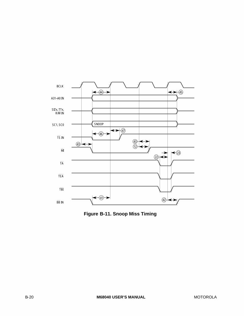
B-20 M68040 USER’S MANUAL MOTOROLA
TBI
TS IN
MI
SIZx, TTx, R/W IN
44
BCLK
A31–A0 IN
TEA
47
SC1, SC0 SNOOP
43
TA
45
2223
BB IN41
42
43
12
46
Figure B-11. Snoop Miss Timing

MOTOROLA M68040 USER’S MANUAL B-21
50
BCLK
12
42
IPEND
RSTO
CDIS
IPL2–IPL0
42
PST3–PST0
12
RSTI
51 52
41
Figure B-12. Other Signal Timing

B-22 M68040 USER’S MANUAL MOTOROLA

MOTOROLA M68040 USER’S MANUAL C-1
APPENDIX CMC68040V AND MC68EC040V
The MC68040V and MC68EC040V are Motorola’s 3.3 volt, static versions of theMC68040 third-generation, M68000-compatible, high-performance, 32-bit microprocessor.They require a 3.3V power supply providing over 50 percent reduction in powerconsumption compared to a 5.0V device. The maximum power used at 3.3 volts is 1.5watts at an operating frequency of 33 MHz. They also have a low-power stop mode. Oncein this state, both devices remain quiescent, consuming less than 330 µW of power. Thelow-power usage of these microprocessors makes them an ideal choice for portablecomputing and power constrained applications.
The MC68040V programming model, data formats and types, instruction set, caches, andMMUs are the same as those described for the MC68LC040 in Appendix A MC68LC040.The MC68EC040V programming model, data formats and types, and instruction set arethe same as those described for the MC68EC040 in Appendix B MC68EC040. However,both devices contain additional features:
• For the MC68040V, all differences that exist between the MC68LC040 and theMC68040, as described in Appendix A MC68LC040, also apply to the MC68040V.For the MC68EC040V, all differences that exist between the MC68EC040 and theMC68040, as described in Appendix B MC68EC040, also apply to theMC68EC040V.
• Both devices operate to 0 Hz and can accept 3.3V or 5V input.
• Both devices have a new processor status state, low-power stop mode, indicatedwhen PST(3–0) = $6.
• There is no PCLK or TRST pin on either device.
• Both devices provide three new pins, system clock disable (SCD), low frequencyoperation (LFO), and loss of clock (LOC).
C.1 ADDITIONAL SIGNALS
Table C-1 lists the additional signals and Figure C-1 illustrates the functional signal groupsof the MC68040V and MC68EC040V.

C-2 M68040 USER’S MANUAL MOTOROLA
Table C-1. Additional MC68040V and MC68EC040V Signals
Signal Name Mnemonic Function
Low FrequencyOperation
LFO Used to enter the low frequency mode of operation.
Loss of Clock LOC Indicates loss of BCLK input, a reset is required
System Clock Disable SCD Indicates normal operation is suspended and low-power stop mode is active,system logic may remove or change the frequency of the BCLK input.
C.1.1 Low Frequency Operation (LFO)
When asserted, this input signal allows the frequency of BCLK to be changedinstantaneously (0 to 16 MHz) providing minimum pulse width constraints are met (seeC.7 MC68040V and MC68EC040V Electrical Characteristics. LFO is only recognizedduring low-power stop mode and reset.
C.1.2 Loss of Clock (LOC)
Whenever the internal clock circuitry detects either a phase lock error or a loss of BCLK,this output signal is driven high (only during normal mode of clocking operation). LOC isalso three-stated during reset, low-power stop, or low frequency operation. There shouldbe a pull-down resistor on the system board to ground.
C.1.3 System Clock Disable (SCD)
When asserted this output signal indicates, when asserted, that the BCLK input can bedisabled or changed in frequency. SCD is asserted upon termination of the LPSTOPbroadcast cycle. BCLK must be stable when SCD is negated, in accordance with thespecifications in C.7 MC68040V and MC68EC040V Electrical Characteristics.

MOTOROLA M68040 USER’S MANUAL C-3
MC68040V MC68EC040V
VCC
GND
BUS ARBITRATIONBGBR
BB
BUS SNOOP CONTROL AND RESPONSE
M I
INTERRUPT CONTROL
IPL0
AVEC
IPEND
PROCESSOR CONTROL
CDIS
RSTIRSTO
BCLK
TEST
TMSTCK
TDI
POWER SUPPLY
TDO
SC0SC1
IPL1IPL2
STATUS AND CLOCKS
PST0PST1PST2
DATA BUS D31–D0
TRANSFER ATTRIBUTES
MASTER TRANSFER CONTROL
A31–A0ADDRESS BUS
TS
TIP
TCI
SLAVE TRANSFER CONTROL
TEA
TBI
R/W
LOCKECIOUT
TT0TT1TM0TM1TM2
TLN0TLN1UPA0UPA1
SIZ0SIZ1
LOCK
TA
MDIS*
PST3
JS0
JS2
LFOLOCSCD
NOTE: *This signal is JS1 on the MC68EC040V.
Figure C-1. MC68040V and MC68EC040V Functional Signal Groups
C.2 LOW-POWER STOP MODE
The low-power stop mode is a reduced power mode of operation, that causes theMC68040V and MC68EC040V to remain quiescent until either a reset or non-maskedinterrupt occurs. This mode of operation has four phases of operation and is triggered bythe low-power stop (LPSTOP) instruction:
1. Perform a LPSTOP broadcast cycle.
2. End integer unit (IU) instruction pipeline sequencing, which is similar to the STOPinstruction sequence (IMM data ˘ SR), at termination of the LPSTOP broadcastcycle.

C-4 M68040 USER’S MANUAL MOTOROLA
3. Orderly shutdown of the clock circuitry, culminating in the low-power stop mode.
4. Return to normal operation after the receipt of a non-masked interrupt or reset whenthe clocks are restarted in an orderly manner.
Once the LPSTOP instruction has reached the execute stage of the IU pipeline and whenall CPU and bus activity has completed, the IU generates an LPSTOP broadcast cycle.Table C-2 lists how the LPSTOP broadcast cycle drives the bus.
Table C-2. Bus Encodings DuringLPSTOP Broadcast Cycle
Signals Encoding Signals Encoding
A31–A0 $FFFFFFFE R/W 0
TT1, TT0 $3 D31–D16 $XXXX
TM2–TM0 $0 D15–D0 #<data>
SIZ1, SIZ0 $2
Either TA or TEA terminates the LPSTOP broadcast cycle. By withholding the assertion ofTA or TEA, external logic can extend the cycle, controlling the beginning of the low-powerstop mode. During this extension, the processor is ready for bus arbitration.
Upon termination of the LPSTOP broadcast cycle, the status register (SR) is updated withthe data portion of the immediate operand (updating the interrupt priority mask level). TheIU updates the processor status lines PST3–PST0 with the new status code of $6 andhalts. Then, SCD is asserted signaling the beginning of the low-power stop mode. Allinstructions in the integer unit pipeline that followed LPSTOP remain in the pipeline duringthe low-power stop mode.
The processor stays in the low-power stop mode until a non-masked interrupt or resetexception occurs. A non-masked interrupt exception is defined as a higher priority than thevalue in the interrupt priority mask bits of the SR, while holding the interrupt priority level(IPL≈) lines until IPEND is asserted. IPL≈ are used in the low-power stop mode to restartthe clocks and return the processor to normal operation. If an interrupt request has apriority higher than the value in the interrupt priority mask bits of the SR, the clock controllogic negates SCD and restarts the PLL. If the pending interrupt has a lower priority thanthe interrupt priority mask bits, the clock logic doesn't restart the PLL and the processorwill not resume normal operation. The MC68040V and MC68EC040V will enter low-powermode regardless of any interrupts that are pending once the LPSTOP instruction starts.
Once the clock control logic negates SCD and the PLL is restarted, a valid BCLK must beprovided to the processor. When the clocks are phase locked, an interrupt, a bus error, ora reset exception begins. The interrupt exception forces all instructions in the pipeline tobe aborted that have not reached the execute stage; while the reset exception aborts anyprocessing in progress (pre-fetched instructions prior to entering low-power stop mode)and cannot be recovered.

MOTOROLA M68040 USER’S MANUAL C-5
C.2.1 Bus Arbitration and Snooping
Bus arbitration and snooping are not allowed during low-power stop mode. If an alternatebus master requires ownership, arbitration must occur before the processor is allowed toenter low-power stop mode. This is achieved by externally decoding the LPSTOPbroadcast cycle and negating the BG signal before the termination of the cycle, allowingbus arbitration to complete at the end of the cycle.
If the MC68040V or the MC68EC040V is the bus master during low-power stop mode,lowest power consumption cannot be achieved due to the DC loads on the processoroutput pins. To achieve maximum power savings, arbitrate bus mastership away from theprocessor during the LPSTOP broadcast cycle.
In a single bus master system the caches do not need to be shut down prior to theexecution of LPSTOP. In a multi-master system, the programmer is responsible forproviding a shut down sequence for the caches.
C.2.2 Low Frequency Operation
In addition to the low-power mode of operation the MC68040V and MC68EC040V providea low frequency mode of operation. This mode of operation can be entered one of in twoways: directly from reset by asserting LFO prior to negating RSTI; or by asserting LFO
prior to generating the interrupt or reset when exiting the low-power stop mode. In theformer case, the BCLK input can be changed as long as the frequency is 0–16 MHz andthe minimum pulse width constraints are met. Normal operation can be resumed throughthe low-power stop mode and deasserting LFO.
C.2.3 Changing BCLK Frequency
The frequency of the BCLK input can be changed only during the low-power stop or lowfrequency modes of operation. Once in the low-power stop mode and SCD is asserted,BCLK can be disabled or its frequency can be changed. Reducing the frequency orremoving the BCLK input is not required for proper operation, but is an additional powersaving measure. BCLK can be removed during the low-power stop mode as an additionalsystem power saving measure. However, it is not necessary for normal operation and hasno effect on the MC68040V's or MC68EC040V's power consumption.

C-6 M68040 USER’S MANUAL MOTOROLA
C.2.4 LPSTOP Instruction Summary
Operation: If Supervisor StateImmediate Data ˘ SRSR ˘ Broadcast CycleSTOP
Else TRAP
Assembler Syntax: LPSTOP #<data>
Attributes: Privileged Word Sized
Condition Codes: Set according to the immediate operand.
Description: See C.2 Low Power Stop Mode.
Instruction Format:
15 14 13 12 11 10 9 8 7 6 5 4 3 2 1 0
1 1 1 1 1 0 0 0 0 0 0 0 0 0 0 0
0 0 0 0 0 0 0 1 1 1 0 0 0 0 0 0
IMMEDIATE DATA
Instruction Fields: Immediate field—Specifies the data to be loaded into the statusregister.

MOTOROLA M68040 USER’S MANUAL C-7
C.3 CLOCKING DURING NORMAL OPERATION
During normal operation of the processor, the BCLK should be driven with a 50% (±5%)duty cycle (refer to C.7 MC68040V and MC68EC040V Electrical Characteristics fordetails). The frequency of BCLK can not be changed during normal operation. Altering theBCLK frequency during normal operation (the LFO signal is negated) will result inunspecified operation. In the event that the BCLK input is lost, a processor reset isrequired. Once the loss of BCLK is detected during normal operation, the processorasserts LOC, indicating a loss of clock. External logic can then reset the processor toresume normal operation.
C.4 RESET OPERATION
An external device asserts the RSTI to reset the processor. When power is applied to thesystem, external circuitry should assert RSTI for a minimum of 10 BCLK cycles after VCCis within tolerance. Figure C-2 is a functional timing diagram of the power-on resetoperation, illustrating the relationships among VCC, RSTI, and bus signals. The BCLKsignal is required to be stable by the time RSTI is negated. The VIH levels of any pin mustnot exceed VCC + 2.5V. RSTI is internally synchronized for two BCLKs before being usedand must meet the specified setup and hold times to BCLK (specifications #51 and #52 inC.7 MC68040V and MC68EC040V Electrical Characteristics) only if recognition by aspecific BCLK rising edge is required. MI is asserted while the MC68040V is in reset.

C-8 M68040 USER’S MANUAL MOTOROLA
BCLK
BUS SIGNALS
+5 V
0 V
RSTI
TS
BR
CDIS, MDIS*,IPL2–IPL0
BG
BB
TIP
VCC
Undefined
t 10 CLOCKS
2 CLOCKS
128 CLOCKS
>
MI
NOTE: * Not on MC68EC040V.
Figure C-2. MC68040V and MC68EC040V Initial Power-On Reset Timing
Once RSTI negates, the processor is internally held in reset for another 124 clocksmaximum. During the reset period, all signals that can be, are three-stated, and the restare driven to their inactive state. Once the internal reset signal negates, all bus signalscontinue to remain in a high-impedance state until the processor is granted the bus.Afterwards, the first bus cycle for reset exception processing begins. Figure C-2 illustratesthat the processor assumes implicit bus ownership before the first bus cycle begins.
For processor resets after the initial power-on reset, RSTI should be asserted for at least10 clock periods. The Figure C-3 illustrates timings associated with a reset when theprocessor is executing bus cycles. Note that BB and TIP (and TA if driven during asnooped access) are negated before transitioning to a three-state level.

MOTOROLA M68040 USER’S MANUAL C-9
BCLK
BUS SIGNALS
RSTI
TS
BR
CDIS, MDIS*,IPL2–IPL0
BG
BB
TIP
t 10 CLOCKS
2 CLOCKS
128 CLOCKS
>
MI
NOTE: * Not on MC68EC040V.
Figure C-3. MC68040V and MC68EC040V Normal Reset Timing
Resetting the processor causes any bus cycle in progress to terminate as if TA or TEA
had been asserted. In addition, the processor initializes registers appropriately for a resetexception. When a RESET instruction is executed, the processor drives the reset out(RSTO) signal for 512 BCLK cycles. In this case, the processor resets the external devicesof the system, and the internal registers of the processor are unaffected. The externaldevices connected to the RSTO signal are reset at the completion of the RESETinstruction. An RSTI signal that is asserted to the processor during execution of a RESETinstruction immediately resets the processor and causes the RSTO signal to negate.RSTO can be logically ANDed with the external signal driving RSTI to derive a systemreset signal that is asserted for both an external processor reset and execution of aRESET instruction. It is necessary that the MC68040V and MC68EC040V be powered upbefore other 5V devices; because the two power supplies must be within 2.5V of eachother.
C.5 POWER CYCLING
In cases were power is cycled off, then on with a duration of one second, RESET must beasserted prior to removing power. This allows for an orderly shutdown within theMC68040V and enables circuitry for the subsequent power-up.
C-10 M68040 USER’S MANUAL MOTOROLA
C.6 MC68040V AND MC68EC040V JTAG (PRELIMINARY)
The MC68040V and MC68EC040V include dedicated user-accessible test logic that isfully compatible with the IEEE standard 1149.1A Standard Test Access Port andBoundary Scan Architecture. Problems associated with testing high-density circuit boardshave led to the standard’s development under the sponsorship of the IEEE TestTechnology Committee and the Joint Test Action Group (JTAG).
The following paragraphs are to be used in conjunction with the supporting IEEEdocument and includes those chip-specific items that the IEEE standard requires to bedefined and additional information specific to the MC68040V and MC68EC040Vimplementations. For example, the IEEE standard 1149.1A test access port (TAP)controller states are referenced in this section but are not described. For these details andapplication information regarding the standard, refer to the IEEE standard 1149.1Adocument.
The MC68040V and MC68EC040V implementations support circuit board test strategiesbased on the standard. The test logic utilizes static logic design and is system logicindependent of the device. The MC68040V and MC68EC040V implementations providecapabilities to:
a. Perform boundary scan operations to test circuit board electrical continuity,
b. Bypass the MC68040V and MC68EC040V by reducing the shift register path to asingle cell,
c. Sample the MC68040V and MC68EC040V system pins during operation andtransparently shift out the result,
d. Disable the output drive to output-only pins during circuit board testing.
NOTE
The IEEE standard 1149.1A test logic cannot be consideredcompletely benign to those planning not to use this capability.Certain precautions must be observed to ensure that this logicdoes not interfere with system operation. Refer to C.6.4Disabling The IEEE Standard 1149.1A Operation.
Figure C-4 illustrates a block diagram of the MC68040V and MC68EC040Vimplementations of IEEE standard 1149.1A. The test logic includes a 16-state dedicatedTAP controller. These 16 controller states are defined in detail in the IEEE standard1149.1A, but only 8 are included in this section.
Test-Logic-Reset Run-Test/IdleCapture-IR Capture-DRUpdate-IR Update-DRShift-IR Shift-DR
Four dedicated signal pins provides access to the TAP controller:
TCK—A test clock input that synchronizes the test logic.
TMS—A test mode select input with an internal pullup resistor sampled on the rising edge of TCK to sequence the TAP controller.
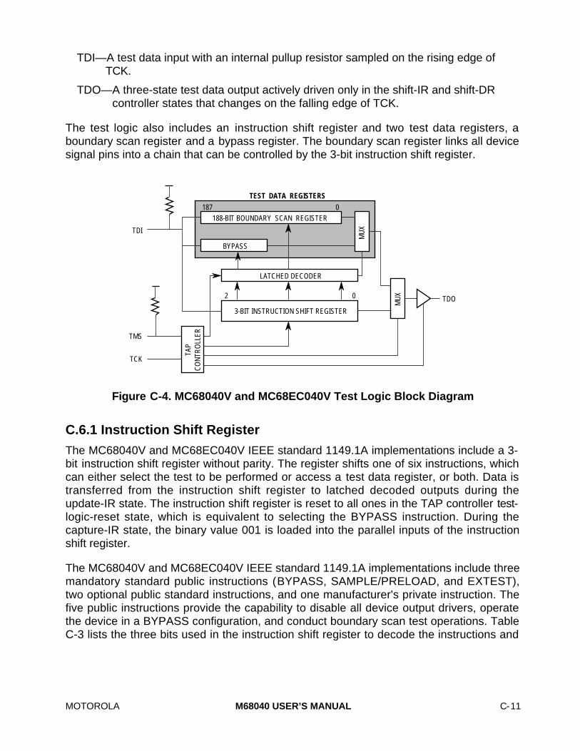
MOTOROLA M68040 USER’S MANUAL C-11
TDI—A test data input with an internal pullup resistor sampled on the rising edge of TCK.
TDO—A three-state test data output actively driven only in the shift-IR and shift-DR controller states that changes on the falling edge of TCK.
The test logic also includes an instruction shift register and two test data registers, aboundary scan register and a bypass register. The boundary scan register links all devicesignal pins into a chain that can be controlled by the 3-bit instruction shift register.
TDI
TDO
TMS
TCK
3-BIT INSTRUCTION SHIFT REGISTER
LATCHED DECODER
188-BIT BOUNDARY SCAN REGISTER
TEST DATA REGISTERS
BYPASS
MU
X
TAP
CO
NTR
OLL
ER
MU
X
187 0
02
Figure C-4. MC68040V and MC68EC040V Test Logic Block Diagram
C.6.1 Instruction Shift Register
The MC68040V and MC68EC040V IEEE standard 1149.1A implementations include a 3-bit instruction shift register without parity. The register shifts one of six instructions, whichcan either select the test to be performed or access a test data register, or both. Data istransferred from the instruction shift register to latched decoded outputs during theupdate-IR state. The instruction shift register is reset to all ones in the TAP controller test-logic-reset state, which is equivalent to selecting the BYPASS instruction. During thecapture-IR state, the binary value 001 is loaded into the parallel inputs of the instructionshift register.
The MC68040V and MC68EC040V IEEE standard 1149.1A implementations include threemandatory standard public instructions (BYPASS, SAMPLE/PRELOAD, and EXTEST),two optional public standard instructions, and one manufacturer's private instruction. Thefive public instructions provide the capability to disable all device output drivers, operatethe device in a BYPASS configuration, and conduct boundary scan test operations. TableC-3 lists the three bits used in the instruction shift register to decode the instructions and

C-12 M68040 USER’S MANUAL MOTOROLA
their related encodings. Note that the least significant bit of the instruction (bit 0) is the firstbit to be shifted into the instruction shift register.
Table C-3. IEEE Standard 1149.1A Instructions
Bit 2 Bit 1 Bit 0 Instruction Selected Test Data Register Accessed
0 0 0 EXTEST Boundary Scan
0 0 1 HIGHZ Bypass
0 1 0 SAMPLE/PRELOAD Boundary Scan
1 0 0 CLAMP Bypass
1 1 0 PRIVATE —
1 1 1 BYPASS Bypass
C.6.1.1 EXTEST. The external test instruction (EXTEST) selects the boundary scanregister. This instruction also activates one internal function that is intended to protect thedevice from potential damage while performing boundary scan operations. EXTESTasserts internal reset for the MC68040V and MC68EC040V system logic to force apredictable benign internal state.
C.6.1.2 HIGHZ. The HIGHZ instruction is an optional instruction provided as a Motorolapublic instruction to anticipate the need to backdrive output pins during circuit boardtesting. The HIGHZ instruction asserts internal system reset, selects the bypass register,and forces all output and bidirectional pins to the high-impedance state.
Holding TMS high and clocking TCK for at least five rising edges causes the TAPcontroller to enter the test-logic-reset state. Using only the TMS and TCK pins and thecapture-IR and update-IR states invokes the HIGHZ instruction. This scheme worksbecause the value captured by the instruction shift register during the capture-IR state isidentical to the HIGHZ opcode.
C.6.1.3 SAMPLE/PRELOAD. The SAMPLE/PRELOAD instruction provides two separatefunctions. First, it provides a means to obtain a sample system data and control signal.Sampling occurs on the rising edge of TCK in the capture-DR state. The user can observethe data by shifting it through the boundary scan register to output TDO using the shift-DRstate. Both the data capture and the shift operations are transparent to system operation.The user must provide some form of external synchronization to achieve meaningfulresults since there is no internal synchronization between TCK and BCLK.
The second function of the SAMPLE/PRELOAD instruction is to initialize the boundaryscan register output cells before selecting EXTEST or CLAMP, which is accomplished byignoring data being shifted out of TDO while shifting in initialization data. The update-DRstate can then be used to initialize the boundary scan register and ensure that known dataand output state will occur on the outputs after entering the EXTEST or CLAMPinstruction.
C.6.1.4 CLAMP. The CLAMP instruction allows the state of the signals driven from theMC68040V and MC68EC040V pins to be determined from the boundary scan register,

MOTOROLA M68040 USER’S MANUAL C-13
while the bypass register is selected as the serial path between TDI and TDO. The signalsdriven from the MC68040V and MC68EC040V pins do not change while the CLAMPinstruction is selected.
C.6.1.5 BYPASS. The BYPASS instruction selects the single-bit bypass register, creatinga single-bit shift-register path from TDI to the bypass register to TDO. The instructionenhances test efficiency when a component other than the MC68040V and MC68EC040Vbecomes the device under test. When the bypass register is initially selected, theinstruction shift register stage is set to a logic zero on the rising edge of TCK followingentry into the capture-DR state. Therefore, the first bit to be shifted out after selecting thebypass register is always a logic zero. Figure C-5 illustrates the bypass register.
1MUX
1
G1
1D
C1
CLOCK DR
FROM TDI
0
SHIFT DR
TO TDO
Figure C-5. Bypass Register
C.6.2 Boundary Scan Register
The 188-bit boundary scan register uses the TAP controller to scan user-defined valuesinto the output buffers, capture values presented to input pins, and control the direction ofbidirectional pins. The instruction shift register cell nearest TDO (i.e., first to be shifted out)is defined as bit zero. The last bit to be shifted out is bit 187. This register includes cellsfor all device signal pins and clock pins along with associated control signals.
The MC68040V and MC68EC040V boundary scan register consists of three cell structuretypes, O.Latch, I.Pin, and IO.Ctl, that are associated with a boundary scan register bit. Allboundary scan output cells capture the logic level of the device output latch during thecapture-DR state. Figures C-6 through C-9 illustrate these three cell types. Figure 6-6illustrates the general arrangement of these cells.

C-14 M68040 USER’S MANUAL MOTOROLA
DATA FROM SYSTEM LOGIC
FROM LAST CELL
CLOCK DR
SHIFT DR TO NEXT CELL
TO OUTPUT BUFFER
1 = EXTEST AND CLAMP 0 = OTHERWISE
1MUX
1
G1
1D
C1
UPDATE BSR
1D
C11MUX
1
G1
Figure C-6. Output Latch Cell (O.Latch)
FROM LAST CELL
TO SYSTEM
LOGIC
SHIFT DRCLOCK DR
TO NEXT CELL
1D
C11
MUX1
G1
INPUT PIN
Figure C-7. Input Pin Cell (I.Pin)

MOTOROLA M68040 USER’S MANUAL C-15
OUTPUT CONTROL FROM SYSTEM LOGIC
FROM LAST CELL
CLOCK DR
SHIFT DR TO NEXT CELL
TO OUTPUT BUFFER (1 = DRIVE)
1 = EXTEST AND CLAMP 0 = OTHERWISE
1D
C1
1MUX
1
G1
1MUX
1
G1
UPDATE BSR
1D
C1
R
RESET
Figure C-8. Output Control Cells (IO.Ctl)
FROM LAST CELL
OUTPUT DATA
INPUT DATA
OUTPUT ENABLE
TO NEXT CELL
TO NEXT PIN PAIR
I/O.CTL
O.LATCH
I.PIN
EN BIDIRECTIONAL PIN
Figure C-9. General Arrangement of Bidirectional Pins

C-16 M68040 USER’S MANUAL MOTOROLA
All MC68040V and MC68EC040V bidirectional pins include two boundary scan data cells,an input, and an output. One of five associated boundary scan control cells controls eachbidirectional pin. If these cells contain a logic one, the associated bidirectional or three-state pin will be configured as an output and enabled. The cell captures the current valueduring the capture-DR state. All five control cells are reset (i.e., logic zero) in the test-logic-reset state. The five bidirectional/three-state control cells, their boundary scanregister bit positions, and the 188 boundary scan bit definitions are not currently available.
C.6.3 Restrictions
Control over the output enable signals using the boundary scan register and the EXTESTand HIGHZ instructions requires a compatible circuit-board test environment to avoiddestructive configurations. The user is responsible for avoiding situations in which theMC68040V and MC68EC040V output drivers are enabled into actively driven networks.
The MC68040V and MC68EC040V include on-chip circuitry to detect the initial applicationof power to the device. Power-on reset (POR, which is an internal signal), the output ofthis circuitry, is used to reset both the system and the IEEE 1149.1A logic. The purpose ofapplying POR to the IEEE 1149.1A circuitry is to avoid the possibility of bus contentionduring power-on. The time required to complete device power-on is power supplydependent. However, the TAP controller remains in the test-logic-reset state while POR isasserted. The TAP controller does not respond to user commands until POR is negated.
The following restrictions apply:1. Leaving the TAP controller test-logic-reset state negates the ability to achieve the
lowest power consumption during the LPSTOP instruction, but does not otherwiseaffect device functionality.
2. The TCK input is not blocked in LPSTOP mode. To consume minimal power, theTCK input should be externally connected to VCC or ground.
3. The TMS and TDI pins include on-chip pull-up resistors. In LPSTOP mode, thesetwo pins should remain either connected to VCC or ground to achieve minimalpower consumption.
4. The external system must assert RSTI within eight bus clocks of exiting from theEXTEST JTAG instruction or else on the tenth bus clock, the MC68040V andMC68EC040V will begin normal reset processing.
C.6.4 Disabling The IEEE Standard 1149.1A Operation
There are two considerations for non-IEEE standard 1149.1A operation. First, TCK doesnot include an internal pullup resistor and should not be left unconnected to preclude mid-level inputs. The second consideration is to ensure that the IEEE standard 1149.1A testlogic remains transparent to the system logic by providing the ability to force the test-logic-reset state. Figure C-10 illustrates a circuit to disable the IEEE standard 1149.1A test logicfor the MC68040V and MC68EC040V.

MOTOROLA M68040 USER’S MANUAL C-17
TDI
TMS
TCLK
TDO NO CONNECTION
+5V
1K
Figure C-10. Circuit Disabling IEEE Standard 1149.1A
C.6.5 MC68040V and MC68EC040V JTAG Electrical Characteristics
The following paragraphs provide information on JTAG electrical and timing specificationsThis section is subject to change. For the most recent specifications, contact a Motorolasales office or complete the registration card at the beginning of this manual.
JTAG DC Electrical Specifications—PRELIMINARY
Characteristic Symbol Min Max Unit
Input High Voltage VIH 2 5.5 V
Input Low Voltage VIL GND 0.8 V
Overshoot — — TBD V
TCK Input Leakage Current @ 0.5–2.4 V Iin TBD TBD µA
TDO Hi-Z (Off-State) Leakage Current @ 0.5–2.4 V ITST TBD TBD µA
Signal Low Input Current, VIL = 0.8 VTMS, TDI
IL TBD TBD mA
Signal High Input Current, VIH = 2.0 VTMS, TDI
IH TBD TBD mA
TDO Output High Voltage IOH = 5ma VOH 2.4 — V
TDO Output Low Voltage IOL = 5ma VOL — 0.5 V
Capacitance*, Vin = 0 V, f = 1 MHz Cin — TBD pF
*Capacitance is periodically sampled rather than 100% tested.

C-18 M68040 USER’S MANUAL MOTOROLA
B
ADRIVE TO 0.5 V
2.0 V
0.8 V
VALID OUTPUT n
VALID OUTPUT n + 1
2.0 V0.8 V
VALID INPUT
2.0 V
0.8 V
2.0 V
0.8 V
DC
DRIVE TO 0.5 V
DRIVE TO 2.4 V
BCLK
OUTPUTS(1)
INPUTS(2)
NOTES:1. This output timing is applicable to all parameters specified relative to the rising edge of the clock.2. This input timing is applicable to all parameters specified relative to the rising edge of the clock.
LEGEND:
A. Maximum output delay specification.B. Minimum output hold time.C. Minimum input setup time specification.D. Minimum input hold time specification.
DRIVE TO 2.4 V
1.5 V 1.5 V
Figure C-11. Drive Levels and Test Points for AC Specifications

MOTOROLA M68040 USER’S MANUAL C-19
This device contains protectivecircuitry against damage due to highstatic voltages or electrical fields;however, it is advised that normalprecautions be taken to avoidapplication of any voltages higherthan maximum-rated voltages to thishigh-impedance circuit. Reliability ofoperation is enhanced if unusedinputs are tied to an appropriatelogic voltage level (e.g., either GNDor VCC).
C.7 MC68040V AND MC68EC040V ELECTRICAL CHARACTERISTICS
The following paragraphs provide information on the maximum rating and thermalcharacteristics for the MC68040V and MC68EC040V. This section is subject to change.For the most recent specifications, contact a Motorola sales office.
C.7.1 Maximum Ratings
Characteristic Symbol Value Unit
Supply Voltage VCC –0.3 to +3.6 V
Input Voltage Vin –0.5 to +5.5 V
Maximum Operating Junction Temperature TJ TBD °C
Minimum Operating Ambient Temperature TA 0 °C
Storage Temperature Range Tstg –55 to 150 °C
C.7.2 Thermal Characteristics
Characteristic Symbol Value Rating
Thermal Resistance, Junction to Case—PGA Package
θJC 3 °C/W
Thermal Resistance, Junction to Case—Surface Mount Package
θJC TBD °C/W
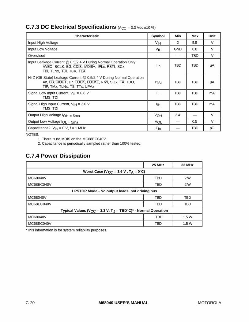
C-20 M68040 USER’S MANUAL MOTOROLA
C.7.3 DC Electrical Specifications (VCC = 3.3 Vdc ±10 %)
Characteristic Symbol Min Max Unit
Input High Voltage VIH 2 5.5 V
Input Low Voltage VIL GND 0.8 V
Overshoot — — TBD V
Input Leakage Current @ 0.5/2.4 V During Normal Operation OnlyAVEC , BCLK, BG, CDIS , MDIS1, IPL≈, RSTI , SCx,TBI, TLNx, TCI , TCK, TEA
Iin TBD TBD µA
Hi-Z (Off-State) Leakage Current @ 0.5/2.4 V During Normal OperationAn, BB, CIOUT , Dn, LOCK , LOCKE, R /W, SIZx, TA, TDO,TIP, TMx, TLNx, TS, TTx, UPAx
ITSI TBD TBD µA
Signal Low Input Current, VIL = 0.8 VTMS, TDI
IIL TBD TBD mA
Signal High Input Current, VIH = 2.0 VTMS, TDI
IIH TBD TBD mA
Output High Voltage IOH = 5ma VOH 2.4 — V
Output Low Voltage IOL = 5ma VOL — 0.5 V
Capacitance2, Vin = 0 V, f = 1 MHz Cin — TBD pF
NOTES:1. There is no MDIS on the MC68EC040V.2. Capacitance is periodically sampled rather than 100% tested.
C.7.4 Power Dissipation
25 MHz 33 MHz
Worst Case (VCC = 3.6 V , TA = 0°C)
MC68040V TBD 2 W
MC68EC040V TBD 2 W
LPSTOP Mode - No output loads, not driving bus
MC68040V TBD TBD
MC68EC040V TBD TBD
Typical Values (VCC = 3.3 V, TJ = TBD°C)* - Normal Operation
MC68040V TBD 1.5 W
MC68EC040V TBD 1.5 W
*This information is for system reliability purposes.

MOTOROLA M68040 USER’S MANUAL C-21
C.7.5 Clock AC Timing Specifications (See Figure C-12)
PRELIMINARY
0 - 16.67 MHz 25 MHz 33 MHz
Num Characteristic Min Max Min Max Min Max Unit
Frequency of Operation 0 16.67 16.67 25 16.67 33 MHz
5 BCLK Cycle Time 60 — 40 60 30 60 ns
6,71 BCLK Rise and Fall Time — 2 — 2 — 2 ns
8 BCLK Duty Cycle Measured at 1.5 V 45 55 45 55 45 55 %
8a2 BCLK Pulse Width High Measured at 1.5 V 28.5 — 18 22 13.63 16.66 ns
8b2 BCLK Pulse Width Low Measured at 1.5 V 28.5 — 18 22 13.63 16.66 ns
9 BCLK edge to edge jitter — — — 20 — 20 ps
NOTES:1. Rising and falling edges of BCLK must be monotonic.2. Specification value at maximum frequency of operation. BCLK must not exceed 16.67 MHz for low
frequency operation
VM
5
6 7
VIH
VILBCLK
8B8A
Figure C-12. Clock Input Timing Diagram
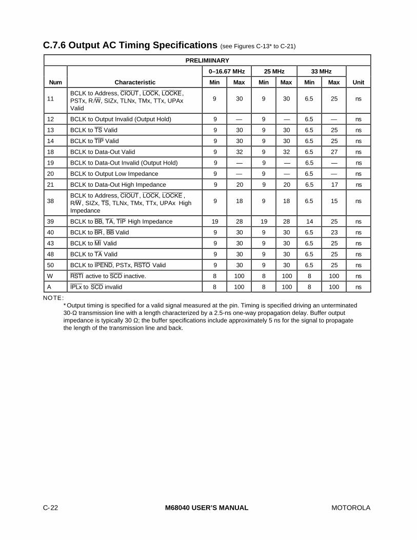
C-22 M68040 USER’S MANUAL MOTOROLA
C.7.6 Output AC Timing Specifications (see Figures C-13* to C-21)
PRELIMIINARY
0–16.67 MHz 25 MHz 33 MHz
Num Characteristic Min Max Min Max Min Max Unit
11BCLK to Address, CIOUT , LOCK, LOCKE ,PSTx, R /W, SIZx, TLNx, TMx, TTx, UPAxValid
9 30 9 30 6.5 25 ns
12 BCLK to Output Invalid (Output Hold) 9 — 9 — 6.5 — ns
13 BCLK to TS Valid 9 30 9 30 6.5 25 ns
14 BCLK to TIP Valid 9 30 9 30 6.5 25 ns
18 BCLK to Data-Out Valid 9 32 9 32 6.5 27 ns
19 BCLK to Data-Out Invalid (Output Hold) 9 — 9 — 6.5 — ns
20 BCLK to Output Low Impedance 9 — 9 — 6.5 — ns
21 BCLK to Data-Out High Impedance 9 20 9 20 6.5 17 ns
38BCLK to Address, CIOUT , LOCK, LOCKE ,R/W , SIZx, TS, TLNx, TMx, TTx, UPAx HighImpedance
9 18 9 18 6.5 15 ns
39 BCLK to BB, TA, TIP High Impedance 19 28 19 28 14 25 ns
40 BCLK to BR , BB Valid 9 30 9 30 6.5 23 ns
43 BCLK to MI Valid 9 30 9 30 6.5 25 ns
48 BCLK to TA Valid 9 30 9 30 6.5 25 ns
50 BCLK to IPEND, PSTx, RSTO Valid 9 30 9 30 6.5 25 ns
W RSTI active to SCD inactive. 8 100 8 100 8 100 ns
A IPL≈ to SCD invalid 8 100 8 100 8 100 ns
NOTE:* Output timing is specified for a valid signal measured at the pin. Timing is specified driving an unterminated30-Ω transmission line with a length characterized by a 2.5-ns one-way propagation delay. Buffer outputimpedance is typically 30 Ω; the buffer specifications include approximately 5 ns for the signal to propagatethe length of the transmission line and back.

MOTOROLA M68040 USER’S MANUAL C-23
C.7.7 Input AC Timing Specifications (See Figures C-13 to C-21)
PRELIMINARY
0–16.67 MHz 25 MHz 33 MHz
Num Characteristic Min Max Min Max Min Max Unit
15 Data-In Valid to BCLK (Setup) 5 — 5 — 4 — ns
16 BCLK to Data-In Invalid (Hold) 4 — 4 — 4 — ns
17 BCLK to Data-In High Impedance (ReadFollowed by Write)
— 49 — 49 — 36.5 ns
22a TA Valid to BCLK (Setup) 10 — 10 — 10 — ns
22b TEA Valid to BCLK (Setup) 10 — 10 — 10 — ns
22c TCI Valid to BCLK (Setup) 10 — 10 — 10 — ns
22d TBI Valid to BCLK (Setup) 11 — 11 — 10 — ns
23 BCLK to TA, TEA, TCI , TBI Invalid (Hold) 2 — 2 — 2 — ns
24 AVEC Valid to BCLK (Setup) 5 — 5 — 5 — ns
25 BCLK to AVEC Invalid (Hold) 2 — 2 — 2 — ns
41a BB Valid to BCLK (Setup) 7 — 7 — 7 — ns
41b BG Valid to BCLK (Setup) 8 — 8 — 7 — ns
41c CDIS , MDIS* Valid to BCLK (Setup) 10 — 10 — 8 — ns
41d IPL≈ Valid to BCLK (Setup) 4 — 4 — 3 — ns
42 BCLK to BB, BG, CDIS , MDIS* , IPL≈ Invalid(Hold)
2 — 2 — 2 — ns
44a Address Valid to BCLK (Setup) 8 — 8 — 7 — ns
44b SIZx Valid to BCLK (Setup) 12 — 12 — 8 — ns
44c TTx Valid to BCLK (Setup) 6 — 6 — 8.5 — ns
44d R/W Valid to BCLK (Setup) 6 — 6 — 5 — ns
44e SCx Valid to BCLK (Setup) 10 — 10 — 11 — ns
45 BCLK to Address SIZx, TTx, R/W , SCxInvalid (Hold)
2 — 2 — 2 — ns
46 TS Valid to BCLK (Setup) 5 — 5 — 9 — ns
47 BCLK to TS Invalid (Hold) 2 — 2 — 2 — ns
49 BCLK to BB High Impedance(Processor Assumes Bus Mastership)
— 9 — 9 — 9 ns
51 RSTI Valid to BCLK 5 — 5 — 4 — ns
52 BCLK to RSTI Invalid 2 — 2 — 2 — ns
B LFO change to valid IPL≈ , RSTI (setup) 5 — 5 — 5 ns
D IPEND valid to IPL≈ invalid (Hold) 0 — 0 — 0 — ns
V RSTI pulse width, leaving LPSTOP mode 10 — 10 — 10 — ns
Z IPL≈, RSTI valid to LFO change (Hold) 500 — 500 — 500 — ns
NOTE: *Not on the MC68EC040V.
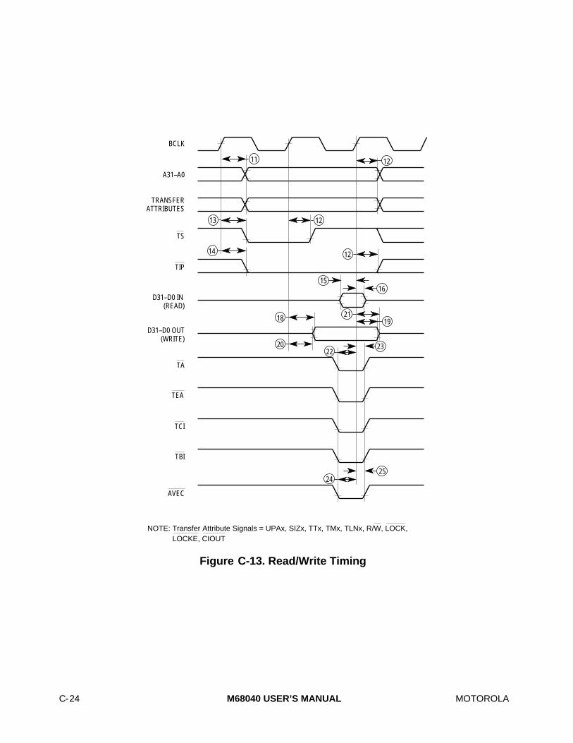
C-24 M68040 USER’S MANUAL MOTOROLA
2223
11
BCLK
A31–A0
TRANSFER ATTRIBUTES
D31–D0 IN (READ)
12
1516
D31–D0 OUT (WRITE)
1921
13 12
14
18
20
TA
TEA
TCI
TBI
TIP
TS
NOTE: Transfer Attribute Signals = UPAx, SIZx, TTx, TMx, TLNx, R/W, LOCK, LOCKE, CIOUT
AVEC
2425
12
Figure C-13. Read/Write Timing

MOTOROLA M68040 USER’S MANUAL C-25
BCLK
A31–A0
TRANSFER ATTRIBUTES
38
20
11
TS
TIP
BB OUT12
39
BG
BR
41 42
12
21
D31–D0 OUT (WRITE)
20
40
13
14
MI
4312
1239
40
NOTE: Transfer Attribute Signals = UPAx, SIZx, TTx, TMx, TLNx, R/W, CIOUT
LOCK, LOCKE
Figure C-14. Bus Arbitration Timing
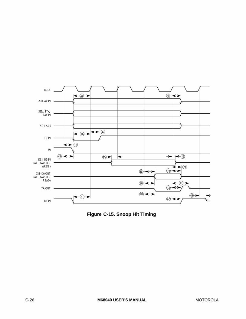
C-26 M68040 USER’S MANUAL MOTOROLA
D31–D0 IN (ALT. MASTER
WRITE)
D31–D0 OUT (ALT. MASTER
READ)
44
BCLK
A31–A0 IN
15 16
4647
12
4148
1220 39
4249
43
1921
18
TS IN
MI
TA OUT
BB IN
SIZx, TTx, R/W IN
45
SC1, SC0
Figure C-15. Snoop Hit Timing

MOTOROLA M68040 USER’S MANUAL C-27
TBI
TS IN
MI
SIZx, TTx, R/W IN
44
BCLK
A31–A0 IN
TEA
47
SC1, SC0 SNOOP
43
TA
45
2223
BB IN41
42
43
12
46
Figure C-16. Snoop Miss Timing
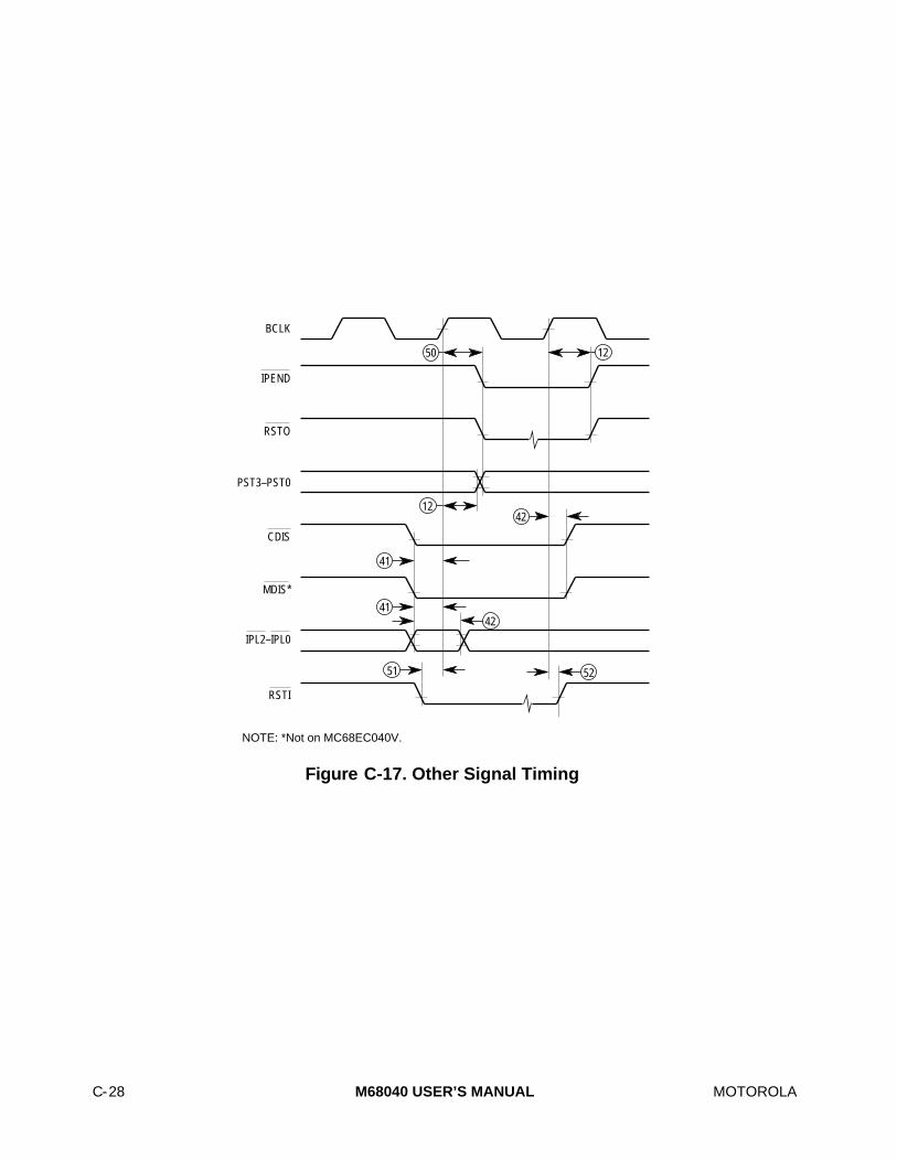
C-28 M68040 USER’S MANUAL MOTOROLA
50
BCLK
12
42
41
IPEND
RSTO
CDIS
MDIS*
IPL2–IPL0
42
PST3–PST0
12
RSTI
51 52
41
NOTE: *Not on MC68EC040V.
Figure C-17. Other Signal Timing
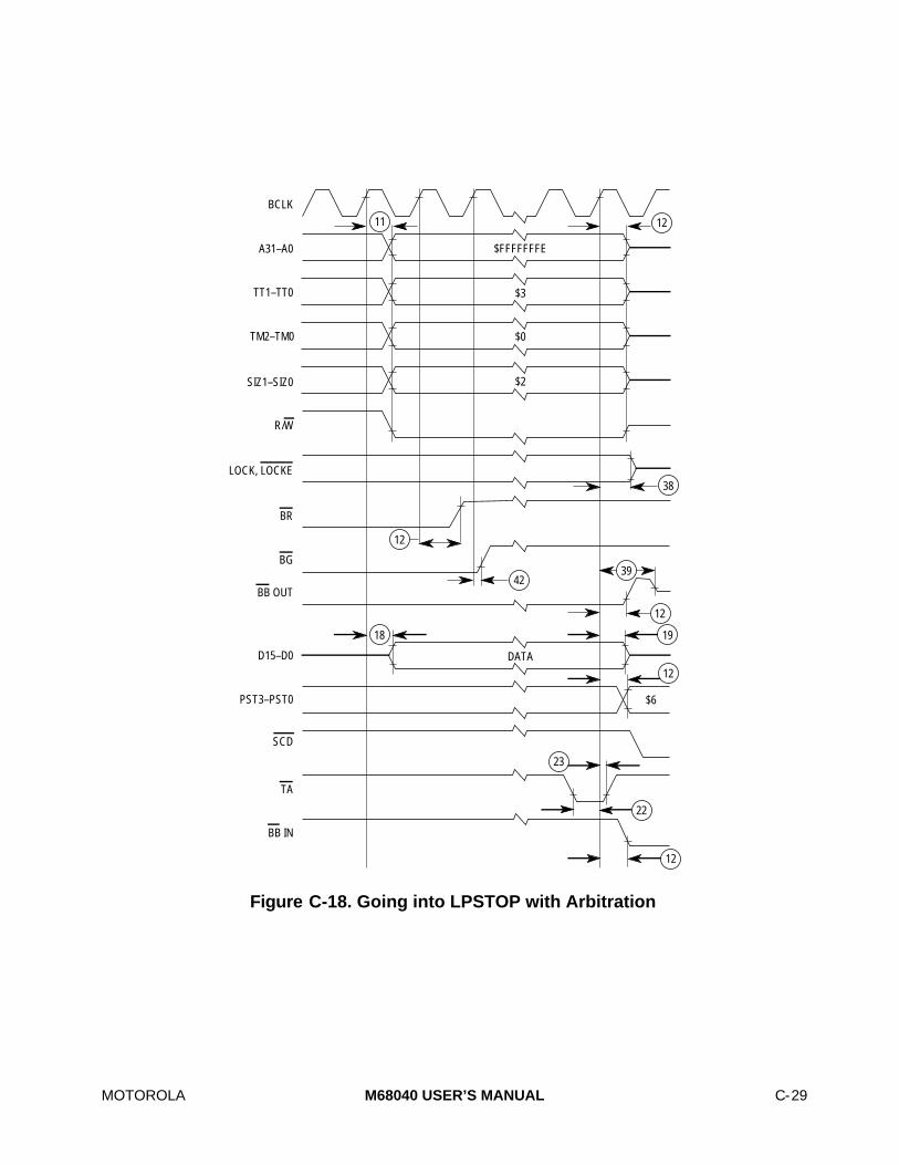
MOTOROLA M68040 USER’S MANUAL C-29
BCLK
A31–A0 $FFFFFFFE
TT1–TT0 $3
TM2–TM0 $0
SIZ1–SIZ0 $2
R/W
BG
D15–D0 DATA
PST3–PST0 $6
TA
BB IN
LOCK, LOCKE
BR
SCD
11 12
38
42
18 19
12
23
22
12
12
BB OUT
12
39
Figure C-18. Going into LPSTOP with Arbitration

C-30 M68040 USER’S MANUAL MOTOROLA
BCLK
$FFFFFFFE
$3
$0
$2
R/W
D15–D0 DATA
PST3–PST0 $6
TA
BG
SCD
1211
BB OUT
A31–A0
TT1–TT0
TM2–TM0
SIZ1–SIZ0
1819
22
23
12
12
BR
Figure C-19. LPSTOP no Arbitration, CPU is Master

MOTOROLA M68040 USER’S MANUAL C-31
BCLK
IPEND
LFO
SCD
IPL2–IPL0 VALID INTERRUPT
124 CLOCKS NORMAL OPERATION
D
A
B
Z
Figure C-20. Exiting LPSTOP with Interrupt
BCLK
LFO
SCD
124 CLOCKSNORMAL
OPERATION
B
V
W
RSTI
Z
Figure C-21. Exiting of LPSTOP with RESET

C-32 M68040 USER’S MANUAL MOTOROLA

MOTOROLA M68040 USER’S MANUAL D-1
APPENDIX DM68000 FAMILY SUMMARY
This appendix summarizes the characteristics of the microprocessors in the M68000family. The M68000PM/AD, M68000 Family Programmer's Reference Manual, includesmore detailed information on the M68000 Family differences.
Attribute MC68000 MC68008 MC68010 MC68020 MC68030 MC68040
Data Bus Size (Bits) 16 8 16 8, 16, 32 8, 16, 32 32
Address Bus Size (Bits) 24 20 24 32 32 32
Instruction Cache (In Bytes) — — 3* (Words) 256 256 4096
Data Cache (In Bytes) — — — — 256 4096
*The MC68010 supports a three-word cache for the loop mode.
Coprocessor Interface
MC68000, MC68008, MC68010 Emulated in Software
MC68020, MC68030 In Microcode
MC68040 Emulated in Software (On-Chip Floating-Point Unit)
Word/Long-Word Data Alignment
MC68000, MC68008, MC68010 Word/Long-Word Data, Instructions, and StackMust Be Word Aligned
MC68020, MC68030, MC68040 Only Instructions Must Be Word Aligned(Data Alignment Improves Performance)
Control Registers
MC68000, MC68008 None
MC68010 SFC, DFC, VBR
MC68020 SFC, DFC, VBR, CACR, CAAR
MC68030 SFC, DFC, VBR, CACR, CAAR, CRP, SRP, TC, TT0,TT1, MMUSR
MC68040 SFC, DFC, VBR, CACR, URP, SRP, TC, DTT0, DTT1,ITT0, ITT1, MMUSR

D-2 M68040 USER’S MANUAL MOTOROLA
Stack Pointer
MC68000, MC68008, MC68010 USP, SSP
MC68020, MC68030, MC68040 USP, SSP (MSP, ISP)
Status Register Bits
MC68000, MC68008, MC68010 T, S, I0/I1/I2, X/N/Z/V/C
MC68020, MC68030, MC68040 T0, T1, S, M, I0/I1/I2, X/N/Z/V/C
Function Code/Address Space
MC68000, MC68008 FC2–FC0 = 7 Is Interrupt Acknowledge Only
MC68010, MC68020, MC68030, MC68040 FC2–FC0 = 7 Is CPU Space
MC68040 User, Supervisor, and Acknowledge
Indivisible Bus Cycles
MC68000, MC68008, MC68010 Use AS Signal
MC68020, MC68030 Use RMC Signal
MC68040 Use LOCK and LOCKE Signal
Stack Frames
MC68000, MC68008 Supports Original Set
MC68010 Supports Formats $0, $8
MC68020, MC68030 Supports Formats $0, $1, $2, $9, $A, $B
MC68040 Supports Formats $0, $1, $2, $3, $7
MC68EC040, MC68LC040 Supports Formats $0, $1, $2, $3, $4, $7
Addressing Modes
MC68020, MC68030, and MC68040 Extensions Memory indirect addressing modes, scaled index, andlarger displacements. Refer to specific data sheetsfor details.

MOTOROLA M68040 USER’S MANUAL D-3
MC68020, MC68030, and MC68040 Instruction Set Extensions
Applies To
Instruction Notes MC68020 MC68030 MC68040
Bcc Supports 32-Bit Displacements
BFxxxx Bit Field Instructions (BCHG, BFCLR, BFEXTS,BFEXTU, BFFFO, BFINS, BFSET, BFTST)
BKPT New Instruction Functionally
BRA Supports 32-Bit Displacement
BSR Supports 32-Bit Displacement
CALLM New Instruction
CAS, CAS2 New Instructions
CHK Supports 32-Bit Operands
CHK2 New Instruction
CINV Cache Maintenance Instruction
CMPI Supports Program Counter Relative Addressing Modes
CMP2 New Instruction
CPUSH Cache Maintenance Instruction
cp Coprocessor Instructions
DIVS/DIVU Supports 32-Bit and 64-Bit Operands
EXTB Supports 8-Bit Extend to 32-Bits
FABS New Instruction
FADD New Instruction
FBcc New Instruction
FCMP New Instruction
FDBcc New Instruction
FDIV New Instruction
FMOVE New Instruction
FMOVEM New Instruction
FMUL New Instruction
FNEG New Instruction
FNOP New Instruction
FRESTORE New Instruction
FSGLDIV New Instruction
FSGLMUL New Instruction
FSAVE New Instruction
FScc New Instruction
FSQRT New Instruction
FSUB New Instruction
FTRAPcc New Instruction
FTST New Instruction
LINK Supports 32-Bit Displacement

D-4 M68040 USER’S MANUAL MOTOROLA
MC68020, MC68030, and MC68040 Instruction Set Extensions (Continued)
Applies To
Instruction Notes MC68020 MC68030 MC68040
MOVE16 New Instruction
MOVEC Supports New Control Registers
MULS, MULU Supports 32-Bit Operands
PACK New Instruction
PFLUSH MMU Instruction
PLOAD MMU Instruction
PMOVE MMU Instruction
PTEST MMU Instruction
RTM New Instruction
TST Supports Program Counter Relative Addressing Modes
TRAPcc New Instruction
UNPK New Instruction
MOTOROLA M68040 USER’S MANUAL E-1
APPENDIX EFLOATING-POINT EMULATION (M68040FPSP)
The MC68040 is user-object-code compatible with the MC68030 and MC68881/MC68882.The MC68040 floating-point unit is optimized to directly execute the most commonly usedsubset of the extensive MC68881/MC68882 instruction set through hardware. Specialtraps and stack frames for the unimplemented instructions and data types provide supportfor the remaining instructions. These functions coupled with Motorola’s floating-pointsoftware package (M68040FPSP) ensure complete user-object-code compatibility.
There are two versions of the M68040FPSP, one for applications compiled for theMC68881/MC68882 (kernel version) and the other for applications compiled for theMC68040 (library version). System integrators can install the kernel version as part of anMC68040-based operating system. The kernel version is used to execute preexisting userobject code written for the MC68881/MC68882 as part of the operating system. Userapplications need not be recompiled or modified in any way once the kernel version isinstalled.
The MC68040 compiler writer and system integrator use the library version which providesless overhead than the kernel version. Overhead is reduced because the appropriatefloating-point exception routine is called directly rather than taking an unimplementedinstruction trap. The library is M68000 application binary interface (ABI) and IEEEexception-reporting compliant; it is not UNIX® exception-reporting compliant.
The M68040FPSP provides the following features:
• Arithmetic and Transcendental Instructions
• IEEE-Compliant Exception Handlers
• MC68040 Unimplemented Data Type and Data Format Handlers
• Can Reside in a 64-Kbyte ROM
• Code Is Reentrant
The M68040FPSP satisfies the IEEE Standard 754 for Binary Floating-Point Arithmetic.The average 25-MHz performance of the transcendental function subroutines is equivalentto that of the 33-MHz MC68881/MC68882. The error bound is equivalent to that of theMC68881/MC68882.
®UNIX is a registered trademark of AT&T Bell Laboratories.

E-2 M68040 USER’S MANUAL MOTOROLA
System designers integrate the M68040FPSP into the system so that the user object coderuns unchanged and remains totally transparent to the end user. The M68040FPSP canbe installed into any operating system. It provides kernel routines to supportunimplemented instructions and unsupported data types. Unimplemented instructions forend-user applications compiled for the MC68881/MC68882 are contained in a library forimproved performance. For all MC68040 floating-point instructions, the coprocessor IDfield must be 001. Table E-1 lists the floating-point functions implemented as instructionsby the MC68040.
Table E-1. MC68040 Floating-Point Instructions
Floating-Point Instructions
Name Description Name Description
FMOVE Move to FPx or CR FDMOVE Double-Precision Move
FSMOVE Single-Precision Move FABS Absolute Value
FCMP Compare FDABS Double-Precision Absolute Value
FSABS Single-Precision Absolute Value FNEG Negate
FTST Test FDNEG Double-Precision Negate
FSNEG Single-Precision Negate FSUB Subtract
FADD Add FMUL Multiply
FDIV Divide FScc Set According to Condition
FBcc Branch Conditionally FTRAPcc Trap Conditionally
FDBcc Test Condition, Decrement, and Branch FSSUB Single-Precision Subtract
FSADD Single-Precision Add FSDIV Single-Precision Divide
FSMUL Single-Precision Multiply FDSUB Double-Precision Subtract
FDADD Double-Precision Add FDDIV Double-Precision Divide
FDMUL Double-Precision Multiply FSSQRT Single-Precision Square Root
FSQRT Square Root FNOP No Operation
FSAVE Save Internal State FSGLMUL Single-Precision Multiply
FMOVEM Move Multiple Registers FRESTORE Restore Internal State

MOTOROLA M68040 USER’S MANUAL E-3
Table E-2 list the arithmetic and transcendental instructions that the M68040FPSPimplements for the MC68040. New instructions have been added to theMC68881/MC68882 base instructions.
Table E-2. M68040FPSP Floating-Point Instructions
Arithmetic Instructions
Name Description Name Description
FADD* Add FSUB* Subtract
FSADD*† Single-Precision Add FSSUB*† Single-Precision Subtract
FDADD*† Double-Precision Add FDSUB*† Double-Precision Subtract
FMUL* Multiply FDIV* Divide
FSMUL*† Single-Precision Multiply FSDIV*† Single-Precision Divide
FDMUL*† Double-Precision Multiply FDDIV*† Double-Precision Divide
FINT Integer Part FINTRZ Integer Part (Truncated)
FABS* Absolute Value FNEG* Negate
FGETEXP Get Exponent FGETMAN Get Mantissa
FTST* Test Operand FCMP* Compare
FREM IEEE Remainder FSCALE Scale Exponent
FMOVE* Move FP Data Register FSMOVE* Single-Precision Move
FDMOVE* Double-Precision Move FSQRT* Square Root
FSSQRT* Single-Precision Square Root FDSQRT* Double-Precision Square Root
FMOD Modulo Remainder FSMOD Single-Precision Modulo Remainder
FDMOD Double-Precision Modulo Remainder
Transcendental Instructions
Name Description Name Description
FCOS Cosine FSIN Sine
FACOS Arc Cosine FASI N Arc Sine
FCOSH Hyperbolic Cosine FSINH Hyperbolic Sine
FSINCOS Simultaneous Sine & Cosine FATAN Arc Tangent
FTAN Tangent FATANH Hyperbolic Arc Tan
FTANH Hyperbolic Tangent FLOG10 Log Base 10
FLOG2 Log Base 2 FLOGNP1 Log Base e of (x + 1)
FLOGN Log Base e FETOXM1 (e to the x Power) –1
FETOX e to the x Power FTWOTOX 2 to the x Power
FTENTOX 10 to the x Power
*The MC68040 provides these functions for all data formats except single, double, and extended denormalized datatypes and extended unnormalized data types. The M68040FPSP provides the functions for the special data types.
†Additional functions not provided by the MC68881/MC68882.

E-4 M68040 USER’S MANUAL MOTOROLA
Table E-3 lists all the data formats and types supported by the MC68040 FPU. Alsoincluded are the data formats and types that the MC68040 FPU does not support but thatare supported by the M68040FPSP.
Table E-3. Support for Data Types and Data Formats
Data Formats
Data Types SGL DBL EXT Decimal Byte Word LongWord
Normalized † † † * † † †
Zero † † † * † † †
Infinity † † † *
NAN † † † *
Denormalized ‡ ‡ * *
Unnormalized * *
* Supported by M68040FPSP†Supported by the MC68040 FPU‡Supported by M68040FPSP after being converted to extended precision by the MC68040 FPU
The M68040FPSP provides system designers with a simple path to port existingMC68881/MC68882 exceptions handlers to the MC68040. It also provides an entry pointfor the IEEE-defined exception conditions listed in Table E-4.
Table E-4. Exception Conditions
Mnemonic Description
BSUN Branch/Set on Unordered
SNAN Signaling Not-a-Number
OPERR Operand Error
OVFL Overflow
UNFL Underflow
DZ Divide by Zero
INEX1/INEX2 Inexact Result 1/2
The M68040FPSP is written in M68000 family assembly code and comes with aninstallation guide. Tape contains both Motorola syntax and UNIX “as” syntax. Tapecartridge (M68040FPSPT) media is available in CPIO and TAR formats. Also available is9-track (M68040FPSPP) media in high or low density as well as CPIO and TAR formats. Alicense is required to obtain rights to use and distribute the M68040FPSP. License termsinclude the right to use and modify source code and redistribute resulting object code.

MOTOROLA M68040 USER’S MANUAL INDEX-1
INDEX
–A–
Access Control Unit, 1-2, B-4, B-5Access Control Unit Register, B-5;
Field Definitions, B-6–B-7Access Error, 1-5, 3-22, 3-23, 3-24, 5-14, 7-37,
7-43, 8-20, 9-21, A-6, A-7, B-11Access Fault, 3-9, 8-6, 8-7Access Serialization, 7-44Acknowledge Bus Cycle
Breakpoint Operation, 7-29, 7-35, 9-20Interrupt Operation, 5-12, 7-31,
7-29–7-35, 8-2Address Bus, 7-1Address Collisions, 7-43Address Error, 7-6, 7-43, 8-8Address Registers, 1-8, 2-4Addressing Modes, 1-10, 2-5, 10-3, 10-4
Brief Extension Word Format, 10-7Full Extension Word Format, 10-7Index Scaling, 1-9, 1-10Index Sizing, 1-9, 1-10Memory Indirect, 2-2Postincrement, 1-9Predecrement, 1-9Program Counter Indirect, 1-9, 1-10Program Counter Relative, 7-6Register Indirect, 1-9, 1-10
Address Translation, 3-1Address Translation Cache, 1-4, 3-2, 3-3, 3-4,
3-7, 3-26, 5-8, 5-14, 8-7, 8-18Address Translation Cache Entry, 3-15, 3-30, 4-2
Field Definitions, 3-27, 3-28Airflow, 11-29, 11-31Alternate Bus Master, 4-1, 4-8, 4-9, 5-4, 5-5, 5-8,
5-9Arithmetic Floating-Point Exceptions,
see Floating-Point ExceptionsAutomatic Test Pattern Generation (ATPG), 6-5Autovector, 7-33, 7-34
–B–
Boundary Scan Control, 6-6, 6-9Breakpoint Operations, 8-12
Bus Cycle, 7-29, 7-35, 9-20BSDL Description, 6-15
Buffer Selection, 7-69Burst Mode Operations, 4-3, 4-11, 5-9Burst Bus Cycles, see Bus CyclesBurst-Inhibited Bus Cycles, see Bus CyclesBus Arbitration, 7-44–7-58
Disregard Request Condition, 7-50Indeterminate Condition, 7-49, 7-58
Bus Arbitration States, 7-46–7-49Explicit Bus Ownership, 7-45Implicit Bus Ownership, 7-67with Direct Memory Access, 7-56
Bus Controller, 1-5, 7-6, 7-10, 7-13, 7-20, 7-45,8-7, 10-8
Bus Cycles,Burst, 5-9, 7-9, 7-10, 7-12, 7-13, 7-22, 7-37,
7-38, 7-42, 7-70Burst-Inhibited, 7-13, 7-22, 7-42, 7-45, 7-60Line, 7-4, 7-9Line Write, 7-22Locked, 5-7, 7-49, 7-53, 7-55, 8-8Push, 4-13Read, 7-4, 7-10, 7-12, 7-32Read-Modify-Write, 3-21, 7-26, 7-41, 7-45, see
also Bus Cycles, LockedWrite, 7-4, 7-20
Bus Error, 3-22, 3-30, 4-12, 7-37, 7-42,7-43,9-21
Bus OperationsAccess Serialization, 7-44Synchronization, 7-44Conditional Branch, 7-50Data Cache, 7-44Double Bus Fault, 8-8, 8-18Exceptions, 8-8Interrupt Pending Procedure, 7-30Locked Transfer, 8-8Misaligned Access, 4-3, 4-11, 10-3Misaligned Operand, 7-6, 7-37Relinquish and Retry, 4-12, 7-41, 7-42, 7-55Reset, 7-66
Bus Synchronization, 7-44BYPASS, 6-3Byte Enable Signals, 7-4
PAL Equation, 7-4Byte Offset, 7-3

INDEX-2 M68040 USER’S MANUAL MOTOROLA
–C–
Cache, 1-4, 2-8Burst Mode Operations, 4-11Data, 2-3, 2-8, 3-1, 3-12, 7-44, 8-7, 8-18Exceptions, 8-7, 8-18Instruction Prefetches, 4-13Instruction, 3-1, 8-7, 8-18Misaligned Accesses, 4-11Page Descriptors, 4-5Replacement Algorithm, 4-4Retry Operation, 4-12Shared Data, 4-9, 4-10
Cache Coherency, 4-10Cache Controller, 3-2, 3-28, 4-4, 4-8, 4-12Cache Inhibited, see Caching ModesCache Line, 4-3
D-Bit, 4-6Dirty, 4-3Format, 4-2Invalid, 4-3; Timing, 10-8V-Bit, 4-3Valid, 4-3
Caching Modes, 4-6Cache Inhibited, 4-7Copyback, 4-6, 7-60Default, 4-6Nonserialized, 4-6Serialized, 4-6Write-Through, 4-6
Caching Operation, 4-3Calculate Stage, see Integer Unit PipelineCM Field, 4-6, 5-8, see also DescriptorsConditional Branch, 7-50Conditional Tests, 9-15, 9-17
Floating-Point IEEE Tests, 9-17, 9-18, 9-25Unordered Conditions, 9-17, 9-18
Control Signals, 7-1, 7-9Copyback, see Caching Modes
–D–
Data Bus, 7-1, 7-3Data Format, 1-9, 9-7
Extended Precision, 9-12, 9-21, 9-23, 9-24Floating-Point Conversion of, 9-12Packed Decimal Real, 9-22
Data Latch Enable (DLE) Mode, 1-2, 5-5, 5-14,7-70, A-5
Data Registers, 2-4Data Types, 9-7
Denormalized Numbers, 1-9, 9-12, 9-22,9-23, 9-16
Infinities, 1-9NANs, 1-9, 9-17Normalized Numbers, 1-9, 9-16, 9-33Unnormalized Numbers, 9-12, 9-22, 9-23Zeros, 1-9
Decode Stage, see Integer Unit PipelineDemand Memory, 3-1Denormalized Numbers, see Data TypesDescriptors, 3-8, 3-12
CM Field, 4-6, 5-8Field Definitions, 3-13Indirect, 3-9, 3-14; PDT Field, 3-17Invalid, 3-9, 3-14M-Bit, 3-21Page, 3-12, 3-13, 3-17, 3-23, 3-24, 4-5Resident, 3-14S-Bits, 3-23Table, 3-12, 3-13, 3-24; UDT Field, 3-19U-Bit, 3-21W-Bits, 3-24
Direct Memory Access (DMA), 7-56Dirty Data, 4-1, 5-8Disabling JTAG, 6-13Disregard Request Condition, 7-55Double Bus Fault, 7-43, 8-8, 8-18DRVCTL.T, 6-3, 6-12Dynamic Bus Sizing, 7-3
–E–
Effective Address (<ea>), 2-3Execute Stage, see Integer Unit PipelineException Handler, 8-4Exception Processing, 1-6, 2-5, 7-36, 7-37, 7-43,
A-6Exception Vector, 2-7
Table, 8-1, 8-4Exceptions
Access Error, 1-5, 3-23, 3-24, 5-14, 7-37,7-43, 9-21, A-6
Access Fault, 3-9, 8-6, 8-7Address Error, 7-6, 7-43, 8-8

MOTOROLA M68040 USER’S MANUAL INDEX-3
Bus Error, 3-22, 3-30, 4-12, 7-37, 7-42, 7-43,9-21
Double Bus Fault, 7-43, 8-8, 8-18F-Line, A-6, B-10Format Error, 8-12, 8-28, 9-20FTRAPcc, 9-20Illegal Instruction, 8-9Interrupt, 5-14, 7-29, 7-31, 8-12, 8-20Memory Management Unit, 8-7Priority, 8-19Privilege Violation, 8-10Reset, 5-11, 7-67, 7-68, 8-17Trace, 8-10Trap, 8-8, 8-20Unimplemented Floating-Point Instruction, 1-2,
9-20Unimplemented Instruction, 8-9
Explicit Bus Ownership, see Bus ArbitrationStates
Extended Precision, see Data FormatExternal Bus Arbiter, 5-7, 5-10, 7-45, 7-46, 7-50,
7-53, 7-55, 7-58EXTEST, 6-3, 6-12
–F–
F-line, A-6, B-10Fetch Stage, see Integer Unit PipelineFloating-Point Exceptions, 1-8, 9-3
Arithmetic, 9-24Branch/Set on Unordered (BSUN), 9-18,
9-25–9-27Divide by Zero, 9-36Floating-Point, 9-5Inexact Result (INEX1 And INEX2), 9-24,
9-36–9-38, 9-42Multiple Exceptions, 9-25Operand Error (OPERR), 9-28–9-31Overflow Exception (OVFL), 9-16, 9-31–9-33,
9-42Round-Off Error, 9-11SNAN Exception, 9-27, 9-28Underflow (UNFL), 9-16, 9-33–9-36, 9-42
Floating-Point Pipeline, 9-1, 9-26Floating-Point Registers
Floating-Point Status Register (FPSR), 1-8,9-4, 9-15AEXC Byte, 9-5; Setting the AEXC, 9-6
EXC Byte, 9-5, 9-13, 9-34, 9-37Floating-Point Registers
FPCC Byte, 9-4Quotient Byte, 9-5
Floating-Point Control Register (FPCR), 1-8,9-3, 9-11, 9-18ENABLE Byte, 9-3, 9-25; Encodings, 9-3MODE Byte, 9-3, 9-31, 9-37
Floating-Point Data Register, 9-2, 9-15Floating-Point Registers
Floating-Point Instruction Address Register(FPIAR), 1-8, 9-6, 9-32, 9-35, 9-38
Floating-Point State Frames, 7-38, 9-39;Field Definitions, 9-42, 9-43
Floating-Point Unit (FPU), 1-2, 1-4Exception Handler, 9-5Floating-Point State Frame, 7-38Format $4 Stack Frame, A-5Integer Pipeline, 10-29Programming Model, 9-2
Floating-Point User Exception HandlerBSUN, 9-26Divide by Zero, 9-36INEX, 9-28, 9-30, 9-32, 9-33, 9-35, 9-37, 9-38OPERR, 9-29, 9-30OVFL, 9-32, 9-33SNAN, 9-28UNFL, 9-35
Floating-Point Vector Numbers, 9-20Forced Rounding Precision, 9-13, 9-31, 9-34Format Error, 8-12, 8-28, 9-20
–H–
Heat Sink, 11-29, 11-31HIGHZ, 6-3, 6-12
–I–
IEEE Aware Tests, see Conditional TestsIEEE Standard 1149.1, see JTAGImplicit Bus Ownership, see Bus Arbitration
StatesIndeterminate Condition, see Bus ArbitrationIndirect Descriptor, see DescriptorsInstruction Execution, 2-5Instruction Timing, 10-1–10-36Instruction Prefetches, 4-13

INDEX-4 M68040 USER’S MANUAL MOTOROLA
InstructionsForced Rounding Precision, 9-13, 9-31, 9-34Privilege Violation Generating, 8-10Trace Exception Generating, 8-10
Integer Unit, 1-4, 2-1, 7-3Supervisor Programming Model, 1-7, 2-5, 2-6User Programming Model, 1-6, 2-4
Integer Unit Pipeline, 1-3, 2-1–2-3, 10-5<ea> Calculate Stage, 1-3, 2-1, 2-2, 10-3,
10-4, 10-6<ea> Fetch Stage, 1-3, 2-1, 2-2, 2-3, 7-4, 10-3Decode Stage, 2-1, 2-2Execute Stage, 2-2, 5-12, 8-1, 8-7, 10-3, 10-4,
10-6Write-Back Stage, 7-43, 10-4, see also Write-
BacksInteger Unit Registers
Address Registers, 1-8, 2-4Cache Control Register (CACR), 1-8, 2-8, 4-5,
8-17Condition Code Register (CCR), 1-8, 2-5;
X-Bit, 2-5Data Registers, 2-4Function Code Registers, 1-8, 2-7Index Registers, 1-8Interrupt Stack Pointer (ISP), 8-4Program Counter (PC), 1-8, 2-5, 8-4Stack Pointer (SP), 1-8, 2-5; Supervisor, 2-6Status Register (SR), 2-7, 8-2
S-Bit, 1-5M-Bit, 2-6, 2-7, 8-4I-Bits, 7-29, 8-13
Vector Base Register (VBR), 1-8, 2-7, 8-4,8-17
Intermediate Result, 9-11, 9-13, 9-15, 9-16, 9-21,9-31, 9-33, 9-37; Format, 9-12
Interrupt Exceptions, 5-14, 7-29, 7-31, 8-12, 8-20Interrupts, 1-5
Acknowledged Bus Cycle, 5-12, 7-29–7-35,7-31, 8-2
Pending Procedure, 7-30Priority Level, 5-11Priority Mask, 7-29, 8-2Request, 8-13Vector Numbers, 8-15
–J–
JTAG (IEEE Standard 1149.1), 5-15, 6-1Boundary Scan Control, 6-6, 6-9BSDL Description, 6-15Disabling, 6-13Electrical And Timing Specifications, 11-1Instructions, see JTAG Instructions
JTAG InstructionsBYPASS, 6-3DRVCTL.T, 6-3, 6-12EXTEST, 6-3, 6-12HI-Z, 6-3, 6-12PRIVATE, 6-3SAMPLE/PRELOAD, 6-3SHUTDOWN, 6-3, 6-12
JTAG Output Drivers, 6-4, 6-5JTAG Registers
Boundary Scan Data Register, 6-2, 6-4, 6-5,6-13
Instruction Shift Register, 6-2–6-6Test Data Register, 6-3, 6-2
JTAG Scan, A-5, B-5Output Drivers, 6-4, 6-5Registers, see JTAG RegistersSystem Clock Restriction, 6-3TAP Controller, 6-1, 6-2, 6-6, 6-13
Junction Temperature, 11-29, 11-30
–L–
Line Filling, 7-6, 7-12, 7-13Line Bus Cycles, see Bus CyclesLocked Bus Cycles, see Bus CyclesLogical Address, 2-3, 2-7, 3-29, 4-3, 3-2, 3-4
Format, 3-8Space, 1-8; Defined 3-29
–M–
M68040FPSP Exception Handler, 9-23BSUN, 9-26OPERR, 9-30OVFL, 9-31, 9-32SNAN, 9-27, 9-28Unimplemented Instruction, 9-35, 9-38

MOTOROLA M68040 USER’S MANUAL INDEX-5
MC68EC0404-Kbyte Page Size, B-4Access Control Registers, see Access Control
UnitAddress Space, B-5DLE Mode, 1-2Electrical Characteristics, 11-19Exception Processing, B-10Multiplexed Bus Mode, 1-2Output Buffer Mode, 1-2Special Modes of Operation, 1-2, B-5Unimplemented Floating-Point Instruction
Exceptions, 1-2, B-10MC68LC040
DLE Mode, 1-2, A-5Electrical Characteristics, 11-15Exception Processing, A-6F-Line Exception, A-6Main Features, A-2Multiplex Bus Mode, 1-2, A-5Output Buffers, A-5Special Modes of Operation, 1-2Unimplemented Floating-Point Instruction
Exceptions, 1-2, A-5Memory Controller, 7-13Memory Management Unit (MMU), 1-4
Cache Controller, 3-2Disable Dynamically, 5-14Memory Controller, 7-13Translation Tables, 3-2
Memory Management Unit Registers, 3-33Initializing, 3-32MMU Status Register (MMUSR), 1-8, 3-3, 3-15
Field Definitions, 3-6, 3-7Status Bits, 3-34
Supervisor Root Pointer (SRP), 1-8, 3-3Translation Control Register (TCR), 1-8, 3-4;
Field Definitions, 3-4; E-Bit 3-33;P-Bit, 3-32, 8-17
Transparent Translation Registers (TTR), 1-4,1-7, 3-2, 3-3, 3-29, 3-30, 4-6, 5-7, 8-17;Field Definitions, 3-5
User Root Pointer (URP), 1-8, 3-3Misaligned Access, 4-3, 4-11, 10-3Misaligned Operand, 7-6, 7-37Multiplexed Bus Mode, 1-2, 5-4, 5-5, 7-69, A-5Multiplexer, 7-3
–N–
NAN, see Data TypesNormalized, see Data Types
–O–
Operand Size, 1-9Output Buffer Mode, 1-2, 7-69, 11-29
–P–
Packed Decimal Real, 9-22Page Descriptor, see DescriptorsPage Index Field (PGI), 3-8Page Size, 3-4, 3-12, 8-17
4 Kbytes, 3-9, 3-29, B-48 Kbytes, 3-6, 3-9, 3-29
Paged Memory, 3-1, 3-21Page Offset Field, 3-8Page State Information, 4-10PDT Field 3-17, see also DescriptorsPhysical Address, 3-2, 3-8, 3-9, 3-29, 4-3
Translation of, see Address TranslationPointer Index Field (PI), 3-8Power Dissipation, 11-29PRIVATE, 6-3Privilege Modes, 1-5
User, 1-6, 2-7Supervisor, 1-6, 2-7, 3-3, 4-5
Processing States, 1-5–1-6Push Bus Cycles, see Bus Cycles
–R–
Range Control, 9-13Read-Modify-Write Bus Cycles, see Bus CyclesRegisters
Floating-Point Unit, see Floating-Point UnitRegisters
Integer Unit, see Integer Unit RegistersJTAG, see JTAG RegistersMemory Management Unit, see Memory
Management Unit RegistersReplacement Algorithm, 4-4Reset Operation, 2-8, 3-4, 3-32, 4-3, 4-5, 5-9,
5-11, 7-66, 9-3, 9-4, 9-6, 9-39, 11-29, 11-30Retry Operation, 4-12, 7-41, 7-42, 7-55Root Index Field (RI), 3-8

INDEX-6 M68040 USER’S MANUAL MOTOROLA
Rounding Algorithm, 9-14Rounding Mode, 9-3, 9-13, 9-16, 9-24, 9-37
Overflow And Underflow, 9-16, 9-30Rounding Precision, 9-3, 9-13, 9-33, 9-37, 9-16
Forced, 9-31, 9-34
–S–
SAMPLE/PRELOAD, 6-3Self-Modifying Code, 4-10Shadow Registers, 2-1SHUTDOWN, 6-3, 6-12Signals
A31–A0, 7-1AVEC, 7-33, 7-34BB, 7-45–7-58BCLK, 6-12, 7-1BG, 7-45–7-58BR, 7-45–7-58CDIS, 4-5, 5-4, 5-5, 7-67, 7-69CIOUT, 4-7D31–D0, 7-1DLE, 1-1, 1-2, 5-5, A-5, B-5IPEND, 5-12, 7-29IPL≈, 7-2, 7-29, 7-34, 7-67, 5-11, 6-5, 8-12,
10-8, A-5, B-8JS0, 1-1, 1-2, A-5, B-5, B-8JS1, 1-2, B-5, B-8LOCK, 3-21, 4-13, 7-26, 7-45–7-58LOCKE, 7-26, 7-45–7-58, 7-54MDIS, 1-2, 3-1, 3-5, 3-32, 5-5, 7-67, B-5, B-8MI, 7-60PCLK, 6-12, 7-1PSTx, 8-18Relationship to System CLOCKs, 7-2RSTI, 3-32, 6-5, 6-6, 6-13, 7-2, 7-66, 7-67,
8-17, B-8RSTO, 8-18SCx, 4-3, 7-60; Encodings 4-9SIZx, 4-13, 7-3, 7-7; Encodings 4-11TA, 4-11, 4-12, 4-13, 8-9, 8-12, 7-60, 8-9,
8-12, 9-20TBI, 4-3, 4-11, 4-12, 4-13, 7-10, 7-20, 7-60TCI, 4-11, 4-12TCK, 6-2, 6-4, 6-6, 6-12TDI, 6-2TDO, 6-2, 6-4, 6-6
TEA, 4-12, 4-13, 7-60, 8-6, 8-7, 8-9,8-12, 9-20
TLNx Encodings, 4-11TMS, 6-2, 6-4TMx, 4-13, 5-6TRST, 6-2, 6-4, 6-13TS, 7-60UPAx, 3-5, 3-15, 3-28,7-60, B-6
Signal Descriptions, 5-2–5-3Sink Data, 4-1, 4-9, 5-8Small Output Buffer, A-5Snoop Controller, 1-4, 5-7Snooping, 4-1, 5-9
Cache Coherency, 4-10Logic, 1-1, 1-5Operation, 5-9
Snoop-Inhibited Operation, 7-61Snooped External Read, 4-8Source Data, 4-1, 4-8, 4-10, 5-8Stack Frames
Access Error, 3-22, 8-20, A-7, B-11;Fields Defined 8-24–8-27
Floating-Point Post-Instruction, A-7, B-11Format $0, 8-21Format $1, 8-21Format $2, 8-22, 9-21, 9-22Format $3, 8-23, 9-31, 9-32, 9-35, 9-38Format $4, 8-23, A-5, B-11Format $7, 8-24MC68LC040, A-5MC68EC040, B-11SSW Field Format Defined, 8-24–8-26
State Data, 4-1, 5-9State Frames, see Floating-Point State FramesSticky Bit, 9-6Supervisor Address Space, 3-23, 8-4Supervisor Mode, see Privilege ModesSynchronization, 7-44Synchronizer Circuit, 7-58
–T–
Table Descriptor, see DescriptorsTable Search, 3-9, 3-12, 3-24, 3-28TAP Controller, 6-1, 6-2, 6-6, 6-13TAP Controller States, 6-3–6-4Tag Entry, see Address Translation Cache EntryThermal Management, 11-29, 11-30, 11-31

MOTOROLA M68040 USER’S MANUAL INDEX-7
Thermal Resistance, 11-29Trace Exceptions, 8-10Trace Mode, 2-7Translation Table, 1-4, 3-2, 3-3, 3-6, 3-7, 3-12,
3-16, 3-32Dynamically Allocated, 3-21Page Frame Address, 3-9Page-Level Tables, 3-7, 3-8Pointer-Level Tables, 3-7Protection Mechanisms, 3-23Root-Level Tables, 3-7Supervisor Root Pointer, 3-23
Transparent Translation, 3-5Transparent Translation Registers,
see Memory Management Unit RegistersTrap Exceptions, 8-8, 8-20
–U–
UDT field 3-19, see also DescriptorsUnimplemented Data Type, 9-22, 9-23, D-2
Exception, 9-20, 9-39Unimplemented Floating-Point Instruction,
9-21, A-6, D-2Exception, 1-2, 9-20, 9-39
Unimplemented Instruction Exceptions,see Exceptions
Unnormalized, see Data TypesUnordered Condition, 9-25User Address Space, 3-23Unsupported Data Types,
see Unimplemented Data TypeUser-Programmable Attribute Bits, 5-7
–V–
VectorNumber, 7-31, 7-33, 7-34, 8-2Offset, 8-15Table, see Exception Vector Table
–W–
Word, see Data FormatWrite Buffer, see BuffersWrite Bus Cycles, see Bus CyclesWrite-Back Stage, see Integer Unit PipelineWrite-Backs, 2-1, 2-3
Block Diagram, 2-3External Write, 2-3
Write-Through, see Caching Modes

INDEX-8 M68040 USER’S MANUAL MOTOROLA