elcodis.com - electronic components...
TRANSCRIPT

Preliminary Data
This is preliminary information on a new product now in development or undergoing evaluation. Details are subject to change without notice.
July 2008 Rev 1 1/43
1
STA680
HD Radio™ base-band receiver
Features
General
■ HD Radio signal decoding for AM and FM digital audio
■ Tensilica™ signal/audio processing core architecture running up to 166 MHz
■ Hardware support for conditional access(one-time programmable 640-bit memory)
■ 2 internal PLLs: processor cores and peripheral bus
■ 1 Internal clock oscillator and external clock input
■ Less than 200 mW with core voltage of 1.2 V and I/O voltage of 3.3 V
■ Temperature range: -40 to +85 °C
Memories
■ Internal boot ROM
■ SDRAM controller addressing up to 512 Mbit of SDRAM in x16 configuration
■ Serial Flash memory interface for application code loading
Turner interface
■ Support of RF-IF peripheral processor (RIPP) and other front ends such as STA3004 and STA7506
■ Input from RF front-end via programmable serial interface supporting 650 kS/s, 675 kS/s, 744.1875 kS/s, 882 kS/s, 912 kS/s sample rates
■ Secondary RF front-end interface for dual tuner applications
Other interfaces
■ One stereo audio sample rate converter(44.1 kS/s, 45.6 kS/s, 48 kS/s)
■ One input and three stereo channels audio output (by IIS serial audio interface)
■ 2 IIC and 3 SPI serial interfaces
■ 1 UART interface
■ 1 GPIO interface (8 lines)
■ SD/MMC interface via SPI
■ JTAG interface
Supported HD Radio system capabilities
■ Multicasting
■ Program service data
■ Real-time traffic
■ Audio time shifting
■ iTunes Tagging ™
■ Surround sound
Applications
■ Car radio
■ Personal navigation device (PND)
■ Portable battery operated systems
LQFP144 (20x20x1.4 mm)LFBGA 168 balls(12x12x1.4 mm)
Table 1. Device summary
Order code Package(1)
1. ECOPACK® compliant.
Packing
STA680 LFBGA 168 balls (12x12x1.4 mm) Tray
STA680Q LQFP144 (20x20mm) Tray
www.st.com
Downloaded from Elcodis.com electronic components distributor

Contents STA680
2/43
Contents
1 Description . . . . . . . . . . . . . . . . . . . . . . . . . . . . . . . . . . . . . . . . . . . . . . . . . 6
2 System overview . . . . . . . . . . . . . . . . . . . . . . . . . . . . . . . . . . . . . . . . . . . . 7
2.1 HD Radio processing . . . . . . . . . . . . . . . . . . . . . . . . . . . . . . . . . . . . . . . . . 8
2.2 Dual stream HD Radio processing . . . . . . . . . . . . . . . . . . . . . . . . . . . . . . . 8
2.3 Additional processing . . . . . . . . . . . . . . . . . . . . . . . . . . . . . . . . . . . . . . . . . 9
2.3.1 AM/FM processing . . . . . . . . . . . . . . . . . . . . . . . . . . . . . . . . . . . . . . . . . . 9
2.3.2 Audio codec . . . . . . . . . . . . . . . . . . . . . . . . . . . . . . . . . . . . . . . . . . . . . . . 9
2.3.3 Other . . . . . . . . . . . . . . . . . . . . . . . . . . . . . . . . . . . . . . . . . . . . . . . . . . . 10
2.4 Overview of main functional blocks . . . . . . . . . . . . . . . . . . . . . . . . . . . . . 10
2.4.1 Adjacent channel filter . . . . . . . . . . . . . . . . . . . . . . . . . . . . . . . . . . . . . . 10
2.4.2 HiFi2 . . . . . . . . . . . . . . . . . . . . . . . . . . . . . . . . . . . . . . . . . . . . . . . . . . . 10
2.4.3 Vectra . . . . . . . . . . . . . . . . . . . . . . . . . . . . . . . . . . . . . . . . . . . . . . . . . . . 10
2.4.4 DMA . . . . . . . . . . . . . . . . . . . . . . . . . . . . . . . . . . . . . . . . . . . . . . . . . . . . 10
2.4.5 Hardware accelerator (VITERBI) . . . . . . . . . . . . . . . . . . . . . . . . . . . . . . 10
3 I/O description . . . . . . . . . . . . . . . . . . . . . . . . . . . . . . . . . . . . . . . . . . . . . 11
3.1 LQFP description . . . . . . . . . . . . . . . . . . . . . . . . . . . . . . . . . . . . . . . . . . . 11
3.2 LFBGA description . . . . . . . . . . . . . . . . . . . . . . . . . . . . . . . . . . . . . . . . . . 12
3.3 Pin list . . . . . . . . . . . . . . . . . . . . . . . . . . . . . . . . . . . . . . . . . . . . . . . . . . . . 13
3.4 I/Os supply groups . . . . . . . . . . . . . . . . . . . . . . . . . . . . . . . . . . . . . . . . . . 20
4 Operation and general remarks . . . . . . . . . . . . . . . . . . . . . . . . . . . . . . . 21
4.1 Clock schemes . . . . . . . . . . . . . . . . . . . . . . . . . . . . . . . . . . . . . . . . . . . . . 21
4.2 Power on . . . . . . . . . . . . . . . . . . . . . . . . . . . . . . . . . . . . . . . . . . . . . . . . . 23
4.2.1 Power supply ramp up phase . . . . . . . . . . . . . . . . . . . . . . . . . . . . . . . . . 23
4.2.2 Oscillator setting time . . . . . . . . . . . . . . . . . . . . . . . . . . . . . . . . . . . . . . 24
4.2.3 Boot sequence . . . . . . . . . . . . . . . . . . . . . . . . . . . . . . . . . . . . . . . . . . . . 24
4.2.4 Normal operation mode . . . . . . . . . . . . . . . . . . . . . . . . . . . . . . . . . . . . . 24
5 Digital I/O and memory interfaces . . . . . . . . . . . . . . . . . . . . . . . . . . . . . 25
5.1 Interfaces: LQFP vs. LFBGA . . . . . . . . . . . . . . . . . . . . . . . . . . . . . . . . . . 25
5.2 Tuner interface . . . . . . . . . . . . . . . . . . . . . . . . . . . . . . . . . . . . . . . . . . . . . 26
Downloaded from Elcodis.com electronic components distributor

STA680 Contents
3/43
5.3 Audio interface (AIF) . . . . . . . . . . . . . . . . . . . . . . . . . . . . . . . . . . . . . . . . . 28
5.3.1 Output serial audio interface (SAI) . . . . . . . . . . . . . . . . . . . . . . . . . . . . . 28
5.3.2 Input serial audio interface . . . . . . . . . . . . . . . . . . . . . . . . . . . . . . . . . . . 29
5.3.3 S/PDIF interface . . . . . . . . . . . . . . . . . . . . . . . . . . . . . . . . . . . . . . . . . . . 29
5.3.4 Audio sample rate converter (ASRC) . . . . . . . . . . . . . . . . . . . . . . . . . . . 30
5.4 Serial peripheral interfaces (SPI) . . . . . . . . . . . . . . . . . . . . . . . . . . . . . . . 30
5.4.1 Host micro serial peripheral interface (SPI1) . . . . . . . . . . . . . . . . . . . . . 31
5.4.2 Flash serial peripheral interface (SPI2) . . . . . . . . . . . . . . . . . . . . . . . . . 32
5.4.3 SD/MMC serial peripheral interface (SPI3) . . . . . . . . . . . . . . . . . . . . . . 32
5.4.4 I2C interfaces . . . . . . . . . . . . . . . . . . . . . . . . . . . . . . . . . . . . . . . . . . . . . 32
5.4.5 Host micro I2C interface (I2C1) . . . . . . . . . . . . . . . . . . . . . . . . . . . . . . . 34
5.4.6 Auxiliary I2C interface (I2C2) . . . . . . . . . . . . . . . . . . . . . . . . . . . . . . . . . 34
5.5 SDRAM interface . . . . . . . . . . . . . . . . . . . . . . . . . . . . . . . . . . . . . . . . . . . 35
6 Electrical specifications . . . . . . . . . . . . . . . . . . . . . . . . . . . . . . . . . . . . . 37
6.1 Absolute maximum ratings . . . . . . . . . . . . . . . . . . . . . . . . . . . . . . . . . . . . 37
6.2 Thermal data . . . . . . . . . . . . . . . . . . . . . . . . . . . . . . . . . . . . . . . . . . . . . . 37
6.3 Operating conditions . . . . . . . . . . . . . . . . . . . . . . . . . . . . . . . . . . . . . . . . 38
7 Package information . . . . . . . . . . . . . . . . . . . . . . . . . . . . . . . . . . . . . . . . 40
8 Revision history . . . . . . . . . . . . . . . . . . . . . . . . . . . . . . . . . . . . . . . . . . . 42
Downloaded from Elcodis.com electronic components distributor

List of tables STA680
4/43
List of tables
Table 1. Device summary . . . . . . . . . . . . . . . . . . . . . . . . . . . . . . . . . . . . . . . . . . . . . . . . . . . . . . . . . . 1Table 2. Pins description . . . . . . . . . . . . . . . . . . . . . . . . . . . . . . . . . . . . . . . . . . . . . . . . . . . . . . . . . 13Table 3. Reference clock configuration . . . . . . . . . . . . . . . . . . . . . . . . . . . . . . . . . . . . . . . . . . . . . . 21Table 4. Power on timing parameters . . . . . . . . . . . . . . . . . . . . . . . . . . . . . . . . . . . . . . . . . . . . . . . . 23Table 5. Interface list . . . . . . . . . . . . . . . . . . . . . . . . . . . . . . . . . . . . . . . . . . . . . . . . . . . . . . . . . . . . 25Table 6. Base-band interfaces pin list. . . . . . . . . . . . . . . . . . . . . . . . . . . . . . . . . . . . . . . . . . . . . . . . 26Table 7. BBI timing values . . . . . . . . . . . . . . . . . . . . . . . . . . . . . . . . . . . . . . . . . . . . . . . . . . . . . . . . 27Table 8. AIF pin list . . . . . . . . . . . . . . . . . . . . . . . . . . . . . . . . . . . . . . . . . . . . . . . . . . . . . . . . . . . . . . 28Table 9. Serial audio interface timing values . . . . . . . . . . . . . . . . . . . . . . . . . . . . . . . . . . . . . . . . . . 29Table 10. SPI interface timing values . . . . . . . . . . . . . . . . . . . . . . . . . . . . . . . . . . . . . . . . . . . . . . . . . 31Table 11. Host Micro SPI pin list. . . . . . . . . . . . . . . . . . . . . . . . . . . . . . . . . . . . . . . . . . . . . . . . . . . . . 31Table 12. Flash SPI pin list . . . . . . . . . . . . . . . . . . . . . . . . . . . . . . . . . . . . . . . . . . . . . . . . . . . . . . . . . 32Table 13. SD/MMC SPI pin list . . . . . . . . . . . . . . . . . . . . . . . . . . . . . . . . . . . . . . . . . . . . . . . . . . . . . . 32Table 14. Host and auxiliary I2C interface pin list . . . . . . . . . . . . . . . . . . . . . . . . . . . . . . . . . . . . . . . . 33Table 15. I2C interface timing values . . . . . . . . . . . . . . . . . . . . . . . . . . . . . . . . . . . . . . . . . . . . . . . . . 33Table 16. I2C1 interface device address . . . . . . . . . . . . . . . . . . . . . . . . . . . . . . . . . . . . . . . . . . . . . . 34Table 17. I2C2 interface device address . . . . . . . . . . . . . . . . . . . . . . . . . . . . . . . . . . . . . . . . . . . . . . 34Table 18. SDRAM Interface pin description . . . . . . . . . . . . . . . . . . . . . . . . . . . . . . . . . . . . . . . . . . . . 35Table 19. SDRAM interface timing values . . . . . . . . . . . . . . . . . . . . . . . . . . . . . . . . . . . . . . . . . . . . . 36Table 20. Absolute maximum ratings . . . . . . . . . . . . . . . . . . . . . . . . . . . . . . . . . . . . . . . . . . . . . . . . . 37Table 21. Thermal data. . . . . . . . . . . . . . . . . . . . . . . . . . . . . . . . . . . . . . . . . . . . . . . . . . . . . . . . . . . . 37Table 22. DC electrical characteristics . . . . . . . . . . . . . . . . . . . . . . . . . . . . . . . . . . . . . . . . . . . . . . . . 38Table 23. Document revision history . . . . . . . . . . . . . . . . . . . . . . . . . . . . . . . . . . . . . . . . . . . . . . . . . 42
Downloaded from Elcodis.com electronic components distributor

STA680 List of figures
5/43
List of figures
Figure 1. Functional data flow diagram . . . . . . . . . . . . . . . . . . . . . . . . . . . . . . . . . . . . . . . . . . . . . . . . 6Figure 2. STA680 block diagram (detailed) . . . . . . . . . . . . . . . . . . . . . . . . . . . . . . . . . . . . . . . . . . . . . 7Figure 3. Single channel application . . . . . . . . . . . . . . . . . . . . . . . . . . . . . . . . . . . . . . . . . . . . . . . . . . 8Figure 4. Dual channel application. . . . . . . . . . . . . . . . . . . . . . . . . . . . . . . . . . . . . . . . . . . . . . . . . . . . 9Figure 5. LQFP pinout (top view) . . . . . . . . . . . . . . . . . . . . . . . . . . . . . . . . . . . . . . . . . . . . . . . . . . . . 11Figure 6. LFBGA ballout (top view) . . . . . . . . . . . . . . . . . . . . . . . . . . . . . . . . . . . . . . . . . . . . . . . . . . 12Figure 7. Clock generation unit . . . . . . . . . . . . . . . . . . . . . . . . . . . . . . . . . . . . . . . . . . . . . . . . . . . . . 22Figure 8. Power on timing . . . . . . . . . . . . . . . . . . . . . . . . . . . . . . . . . . . . . . . . . . . . . . . . . . . . . . . . . 23Figure 9. BBI waveforms and timings . . . . . . . . . . . . . . . . . . . . . . . . . . . . . . . . . . . . . . . . . . . . . . . . 27Figure 10. Serial audio interface waveforms and timings . . . . . . . . . . . . . . . . . . . . . . . . . . . . . . . . . . 29Figure 11. Three SPI timing diagrams and waveform . . . . . . . . . . . . . . . . . . . . . . . . . . . . . . . . . . . . . 31Figure 12. Timing diagrams and waveform for the two I2C interfaces . . . . . . . . . . . . . . . . . . . . . . . . . 33Figure 13. Timing diagrams and waveform for the SDRAM interface . . . . . . . . . . . . . . . . . . . . . . . . . 35Figure 14. LQFP144 (20x20mm) mechanical data and package dimensions . . . . . . . . . . . . . . . . . . . 40Figure 15. LFBGA 168 balls (12x12x1.4 mm) mechanical data and package dimensions . . . . . . . . . 41
Downloaded from Elcodis.com electronic components distributor

Description STA680
6/43
1 Description
The STA680 from STMicroelectronics is a system on a chip designed for demodulating and decoding of HD Radio(a) signals. The STA680 is compliant with the IBiquity specification and extends the possibility to implement new and optional features and to manage additional services.
The device combines it all into a single IC consisting of several hardware blocks and a programmable core to guarantee the proper level of flexibility, low current consumption and an optimized die size.
The STA680 implements the entire signal processing chain of an HD Radio receiver.
● The digital channel demodulation and decoding, including OFDM demodulation and error correction.
● Source decoding, consisting of audio and data decoding of the digital channel.
● The analog demodulator extracting the audio signal from the legacy analog AM/FM signal (can be implemented as an optional feature)
● The blending of the analog and digital audio signals
Figure 1 presents a functional diagram describing the data flow inside STA680 for HD Radio demodulating and decoding.
The architecture consists of an effective and balanced hardware/software implementation, to pursue the best combination in terms of current consumption, system flexibility and device cost.
Functional blocks which are standard, and computation intensive, are implemented using custom logic. Software implementation is more efficient for functional blocks where flexibility is needed. Such flexibility enables the STA680 to be ready for future evolution, and allows the implementation of specific and optional features.
Figure 1. Functional data flow diagram
a. HD Radio™ technology manufactured under license from iBiquity Digital Corp. U.S. and Foreign Patents. HD Radio™ and the HD Radio logo are proprietary trademarks of iBiquity Digital Corp.
AC00175
SR
C
Main BB Interface
SR
C
Main BB Interface
SR
C
SecondaryBB Interface
SR
C
SecondaryBB Interface
OFDMDemod
PSK/QAMDemod
Deinterleaverand
ConvolutionalDecoding
Channel Decoder
OFDMDemod
PSK/QAMDemod
Deinterleaverand
ConvolutionalDecoding
Channel Decoder
Digital
Digital
Analog AM/FMDemodulation
DE
MU
X
HDCDecoder
Data Processing
Source Decoder
Blending
Blended Audio Sam
ple Rate C
onverter and Serial Interfaces
Audio Samples
DATA
I2S
SPI
I2C
BBI1
BBI2
I2S
**
* This features may be performed outside STA680 depending on the software configuration
Legacy AM/FM Samples STA680
Downloaded from Elcodis.com electronic components distributor

STA680 System overview
7/43
2 System overview
Figure 2 shows the partitioning of the HD Radio receiver system, composed by an AM/FM RF front-end, IF channel signal processor and the HD Radio decoder (STA680).
Figure 2. STA680 block diagram (detailed)
The analog IF signal from the tuner front-end is digitized by a high-resolution sigma-delta A/D converter. A digital down-converter block, embedded into the IF channel signal processor, transforms the IF into a complex base-band signal. Its Bandwidth and sample rate have been adapted by filtering and decimation to match the specification of the HD Radio system. The complex base-band signal feed the HD Radio decoder (STA680) where the HD Radio stream is demodulated and decoded. The STA680 receives a digital base-band signal from the IF channel signal processor and returns the recovered audio and data services.
STA680 can be configured to work with digital IF base-band inputs based on standard front-ends. Front-ends must conform to HD Radio standards for filter bandwidth and linearity.
The STA680 requires external serial Flash memory to boot but can also be configured to boot from a host controller on IIC or SPI interfaces. The FLASH memory Is issued for program code and configuration data storage. STA680 needs SDRAM for bulk data storage required during the IBOC signal processing.
CoreSystem
I/O & ControlInterface
BBI 1
I2S
AM/FM BasebandTuner
(i.e. STA3004)
RF Tuner(i.e. TDA7528)
BaseBandInterface
Peripheral Bus
AHB Bus
AudioInterface
Vectra LXTensilica DSP
HiFiTensilica Core
Viterbi DMA
SPIFlash
SPISD/MMC GPIO
Clock Gen. Unit
SystemPLL
PeripheralPLL
LDO
CrystalOscillator
Opt. Xtal 28.224 MHz
STA680
AHB/APBBridge
Slave Connection
Master Connection
1MBSERIAL FLASH
(bootable)8 Mbit (1Mx8)
MMC,SDSDIOCards(4/8bit)
MMC,SDSDIOCards(4/8bit)
MAIN MICRO
SDRAMInterface
8MBSDRAM
64 Mbit (4Mx16)
OTP
SPI/I2CMicro i/f
Boundary ScanJTAG
Tuner & AudioInterface
BBI 2
Downloaded from Elcodis.com electronic components distributor

System overview STA680
8/43
2.1 HD Radio processingThe STA680 HD Radio Decoder does the processing of the IBOC signal. It receives a complex digital signal from an AM/FM IF channel signal processor. The native sample rate is 744.1875 kS/s for FM and 46.51171875 kS/s for AM. However, other input sample rates are acceptable because of the sample rate converter in the base-band Interface (BBI). These include: 650 kS/s, 675 kS/s, 882 kS/s and 912 kS/s. If a base-band signal is provided that is not at the native sample frequency of 744.1875 kHz it must be sample rate converted to this rate. Sample rate conversion hardware is provided on-chip to support this. This feature allows the STA680 to operate with various AM/FM front-ends.
The STA680is then responsible for detection, acquisition, and demodulation of the IBOC signal. Such function is primarily implemented by the Vectra DSP core. The demodulated signal is then passes to the Hi-Fi processor, for decoding, audio blending and handling of data services. A digital 44.1 kHz decompressed audio is output via the Digital Audio Interface.
The STA680 uses sophisticated algorithms to recover IBOC data even in the presence of signal impairments including fading and a variety of other interferences.
To process the HD Radio stream STA680 requires a 4Mx16 external SDRAM (with up to 32Mx16 supported) for data storage.
2.2 Dual stream HD Radio processingSTA680 is capable to simultaneously demodulate two different HD Radio streams. This unique feature enables the device to decode an HD Radio audio stream, in parallel with any data service broadcasted by a different radio channel. The implementation of the dual stream HD Radio processing requires that two AM/FM RF tuners are connected to the STA680.
In a single channel implementation a single RF tuner is used. In such configuration STA680 is able to demodulate at the same time both the audio and the data associated with the radio channel (i.e. 92.5 MHz or 102.5 MHz). This means that if the user sets the tuner 102.5 MHz, he or she can listed to FM2 audio and receive traffic information broadcasted on that channel. At the same time if the user tunes to another frequency (FM1), current traffic information will be lost.
Figure 3. Single channel application
FM1 Audio
FM1News
FM 1
FM1 Audio
FM1News
FM 1
FM2 Audio
FM2Traffic
FM 2
FM2 Audio
FM2Traffic
FM 2
92.5 102.5 MHz
FM1 News
FM1Audio
FM1 News
FM1Audio
FM2 Traffic
FM2Audio
FM2 Traffic
FM2Audio
OR
Data received are bound to the selected Audio channel
Downloaded from Elcodis.com electronic components distributor

STA680 System overview
9/43
In a dual channels implementation STA680 can simultaneously demodulate audio and data associated to different radio channels. This means that in the example above it would be still possible to receive traffic information broadcasted on FM2 (102.5 MHz) while listening FM1 audio program broadcasted on 92.5 MHz
Figure 4. Dual channel application
2.3 Additional processingThe HD Radio stream demodulation and decoding take up only part of the computation power and memories resources available on STA680. This makes it possible to use the spare resources to implement additional features.
Depending on memory and computation power required by the additional features, it is possible to run them in parallel with the HD Radio stream decoding or in alternative, having all the hardware resources available for the additional features.
2.3.1 AM/FM processing
It is possible to implement legacy AM/FM processing in parallel with the HD Radio stream demodulation and decoding. Such solution is particularly suitable and appealing when the STA680 processor works jointly with an AM/FM RF front-end not incorporating the AM/FM demodulation.
2.3.2 Audio codec
STA680 can be used as a media processor to decode MP3/WMA audio stream. Thanks to the availability of the MMC and SD interface it is possible to reproduce an MP3 stream stored into any MMC or SD cards
FM1 Audio
FM1News
FM 1
FM1 Audio
FM1News
FM 1
FM2 Audio
FM2Traffic
FM 2
92.5 102.5 MHz
FM1 News
FM1Audio
FM1 News
FM1Audio
OR
Audio and Data can belong to different channels
FM2 Traffic
FM1Audio
OR
FM1 News
FM2Audio
OR
FM2 Traffic
FM1Audio
Downloaded from Elcodis.com electronic components distributor
System overview STA680
10/43
2.3.3 Other
The spare computation power and memories are suitable to implement other specific algorithms or custom software application. For example sophisticated sound and audio processing could be implemented on the HD Radio decompressed audio. Audio output can be provided either in IIS master clock mode or in slave mode with the on-chip audio sample rate converter. Up to six audio channels may be provided in a standard configuration.
Another possibility is to implement on the STA680 the handling of data services.
2.4 Overview of main functional blocks
2.4.1 Adjacent channel filter
This module performs time domain filtering specifically for IBOC system. It receives a complex base-band IBOC signal input from SRC module and pre-conditions the signal for subsequent modem processing. The module is a front end device.
2.4.2 HiFi2
The HiFi2 is a signal processing engine specifically designed to provide high quality 24-bit audio processing. The HiFi2 is also useful for advanced data applications such as storage and playback of received audio and conditional access processing. The HiFi2 leverages the Tensilica Xtensa LX engine with additional useful hardware capabilities such as:
● Specialized instructions for 24-bit Audio MAC & stream coding
● Dual MAC (each supports 24x24 and 32x16 bit format)
● Huffman Encode / Decode and truncate functions
● Two way SIMD arithmetic and Boolean operations
2.4.3 Vectra
The Vectra LX is a powerful, configurable 32-bit RISC engine optimized for DSP with VLIW capabilities. The Vectra LX on board the STA680 includes eight MAC units, sixteen 160-bit vector operation registers, and a number of SIMD arithmetic instructions. Custom instructions in the Vectra are targeted for DSP applications such as filters and FFTs. The Vectra processor has been further configured with specific instructions for efficient performance on the HD Radio application.
2.4.4 DMA
A ten-channel DMA controller is attached to the AHB bus to allow the Vectra and HiFi2 processor cores to move large blocks of data efficiently. Certain channels are dedicated for use with certain hardware blocks because of hardware handshaking signals.
2.4.5 Hardware accelerator (VITERBI)
A complex convolutional Viterbi module is designed to fully comply with the HD Radio system. The module supports both K constant of 7 and 9, for IBOC digital FM and AM bands respectively.
Downloaded from Elcodis.com electronic components distributor

STA680 I/O description
11/43
3 I/O description
The STA680 has two package options to suit different application needs. The first option is a 20x20mm LQFP package with 144 pins while the second one is a 12x12mm LFBGA with 169 balls and 0.8mm pitch.
3.1 LQFP descriptionFigure 5 presents the pinout of the STA680 for the LQFP package option. Different colors have been used for I/O signals from different interfaces according to Table 2 reported in Section 3.3.
Figure 5. LQFP pinout (top view)
VD
D
GN
D
SD
R_A
3
SD
R_A
2
SD
R_A
1
SD
R_A
0
SD
R_A
10
GN
D_R
AM
_IO
VD
D_R
AM
_IO
SD
R_B
A1
SD
R_B
A0
SD
R_C
S_N
GN
D
VD
D
SD
R_R
AS
SD
R_C
AS
SD
R_W
E_N
SD
R_A
4
GN
D_R
AM
_IO
VD
D_R
AM
_IO
SD
R_A
5
SD
R_A
6
SD
R_A
7
GN
D
VD
D
SD
R_A
8
SD
R_A
9
SD
R_A
11
SD
R_A
12
GN
D_R
AM
_IO
VD
D_R
AM
_IO
SD
R_C
KE
SD
R_D
QM
1
SD
R_D
QM
0
GN
D
VDD
SDR_D7
SDR_D6
SDR_D5
VDD_RAM_IO
GND_RAM_IO
SDR_D4
SDR_D3
SDR_D2
VDD
GND
SDR_D1
SDR_D0
SDR_D8
SDR_D9
VDD_RAM_IO
GND_RAM_IO
SDR_D10
SDR_D11
SDR_D12
VDD
GND
SDR_D13
SDR_D14
SDR_D15
SDR_FEED_CLK
SDR_CLK_RAM3V3
VDD_RAM_IO_1V8
GND_RAM_IO_1V8
GND
VDD
SPI2_MISO
SPI2_SCK
SPI2_SS0_N
SPI2_MOSI
VDD_FSH_IO
GN
D
GN
D_G
EN
_IO
VD
D_G
EN
_IO
BB
1_I
BB
1_W
S
BB
1_B
CK
SP
DIF
AU
DIO
_IN
_AB
CK
AU
DIO
_IN
_AW
S
VD
D
GN
D
GN
D_G
EN
_IO
VD
D_G
EN
_IO
AU
DIO
_IN
_AD
AT
DA
C25
6X
AD
AT
3
AD
AT
2
AD
AT
AW
S
AB
CK
CLK
_IN
GN
D
VD
D
GN
D_P
LL
_DIG
VD
D_P
LL
_DIG
GN
D_P
LL
0_A
NA
VD
D_P
LL
0_A
NA
GN
D_O
SC
VD
D_O
SC
OS
C_I
N
OS
C_O
UT
VD
D_R
EG
3V3
VD
D_R
EG
1V8
GN
D
VD
D
GN
D_F
SH
_IO
144
143
141
140
139
138
137
136
135
134
133
132
131
130
129
128
127
126
125
124
123
122
121
120
119
118
117
116
115
114
113
112
111
110
109
1 108
2 107
3 106
4 105
5 104
6 103
7 102
8 101
9 100
10 99
11 98
12 97
13 96
14 95
15 94
16 93
17 92
18 91
19 90
20 89
21 88
22 87
23 86
24 85
25 84
26 83
27 82
28 81
29 80
30 79
31 78
32 77
33 76
34 75
35 74
36 73
37 38 39 40 41 42 43 44 45 46 47 48 49 50 51 52 53 54 55 56 57 58 59 60 61 62 63 64 65 66 67 68 69 70 71 72
142
TESTMODE
TRST_N
TCK
TMS
TDI
TDO
RTS_GPIO0
VDD
GND
CTS_GPIO1
GND_GEN_IO
VDD_GEN_IO
TXD_GPIO2
RXD_GPIO3
RESET_N
SPI1_SS0_N
SPI1_SCK
SPI1_MOSI
VDD
GND
SPI1_MISO
GND_GEN_IO
VDD_GEN_IO
IIC1_SCL
IIC1_SDA
BB2_Q
GND
VDD
GND_GEN_IO
VDD_GEN_IO
BB2_I
BB2_WS
BB2_BCK
BLEND
BB1_Q
VDD
AC00504
Color legenda: SDRAM Interface
IIS Tuner Interfaces
Flash/Card Interfaces
Host Processor Interfaces
GPIO & UART Interfaces
IIS Audio Input Interface
Audio Output Interfaces
Downloaded from Elcodis.com electronic components distributor

I/O description STA680
12/43
3.2 LFBGA descriptionFigure 6 presents the ballout of the STA680 for the LFBGA package option. Different colors have been used for I/O signals from different interfaces according to Table 2 reported in Section 3.3.
Figure 6. LFBGA ballout (top view)
1 2 3 4 5 6 7 8 9 10 11 12 13 14
A
B
C
D
E
F
G
H
J
K
L
M
N
P
GPIO6 BB2_BCK BB2_I GND_IO_GEN IIC1_SDA SPI1_MISO SPI1_SCK RESET_N TXD_GPIO2 RTS_GPIO0 VDD_GEN_IO TESTMODE
GPIO5 BB1_Q BLEND BB2_WS GND_IO_GEN BB2_Q IIC1_SCL SPI1_MOSI SPI1_SS0_N RXD_GPIO3 CTS_GPIO1 VDD_GEN_IO SDR_A3SDR_A3 TRST_NTRST_N
BB1_WS BB1_I ADAT2 IIC2_SDA GPIO7 IIC2_SCL IIC1_DA SPI3_MOSI SPI3_MISO SPI3_SCK TDI TCK SDR_A1SDR_A1 SDR_A2SDR_A2
VDD_GEN_IO VDD_GEN_IO BB1_BCK IIC2_DA VDD VDD SPI3_SS_N GPIO4 TDO TMS SDR_A10SDR_A10 SDR_A0SDR_A0
AUDIO_IN_ABCK
SPDIF ADAT3 VDD_PLL_DIG VDD MODEOP_FSH SDR_BA0SDR_BA0 SDR_BA1SDR_BA1
AUDIO_IN_ADAT
AUDIO_IN_AWS
GND_PLL_DIG
GND_PLL_ DIG
GND GND GND GND VDD MODEOP_GEN SDR_RAS_NSDR_RAS_N SDR_CS_NSDR_CS_N
AWS ADAT DAC256X GND GND GND GND SDR_CAS_NSDR_CAS_N SDR_WE_NSDR_WE_N VDD_RAM_IOVDD_RAM_IO
GND_IO_GEN GND_IO_GEN ABCK GND GND GND GND SDR_A4SDR_A4 SDR_A5SDR_A5 GND_RAM_IOGND_RAM_IO
VDD_OSC GND_OSC GND_PLL1_ANA
GND_PLL0_ANA
GND GND GND GND VDD VDD SDR_A7SDR_A7 SDR_A6SDR_A6
OSC_OUT CLK_IN VDD VDD_REG3V3 VDD VDD SDR_A9SDR_A9 SDR_A8SDR_A8
OSC_IN GND_OSC VDD VDD_REG3V3 VDD_FSH_IO GND_FSH_IO VDD_RAM_IO_1V8
GND_RAM_IO_1V8
GND_RAM_IO GND_RAM_IO SDR_A12SDR_A12 SDR_A11SDR_A11
VDD_PLL1_ANA
VDD_PLL0_ANA
SPI2_SS1_N SPI2_SS2_N SPI2_SS3_N SDR_CLK_ RAM1V8
SDR_D13 SDR_D10 VDD_RAM_IO VDD_RAM_IO GND_RAM_IO GND_RAM_IO SDR_DQM1 SDR_CKE
VDD_REG1V8 VDD_REG1V8 SPI2_MOSI SPI2_SCK SDR_CLK_RAM3V3
SDR_D15SDR_D15 SDR_D12SDR_D12 SDR_D9SDR_D9 SDR_D0SDR_D0 SDR_D2SDR_D2 SDR_D4SDR_D4 SDR_D6SDR_D6 SDR_DQM0
SPI2_SS0_N SPI2_MISO SDR_FEED_CLK
SDR_D14SDR_D14 SDR_D11SDR_D11 SDR_D8SDR_D8 SDR_D1SDR_D1 SDR_D3SDR_D3 SDR_D5SDR_D5 SDR_D7SDR_D7
Ball unused Ball not present
AC00707
Color legenda:
SDRAMInterface
IIS TunerInterfaces
Flash/CardInterfaces
Host ProcessorInterfaces
GPIO & UARTInterfaces
IIS Audio InputInterface
Audio OutputInterfaces
Downloaded from Elcodis.com electronic components distributor

STA680 I/O description
13/43
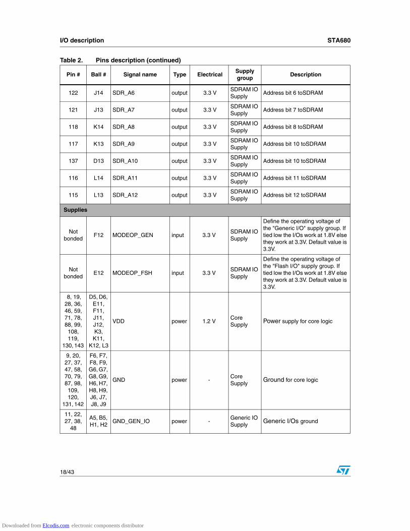
3.3 Pin listThe Table 2 briefly describes the main function and characteristics of the STA680 I/O signals in normal operation mode.
Table 2. Pins description
Pin # Ball # Signal name Type Electrical Supplygroup
Description
Test
1 A13 TESTMODE input 1.8 V or 3.3 VGeneric IO Supply
Factory test mode
Standard 1149.1 JTAG interface
2 B14 TRST_N input 1.8 V or 3.3 VGeneric IO Supply
JTAG active-low test reset
3 C12 TCK input 1.8 V or 3.3 VGeneric IO Supply
JTAG test clock
4 D12 TMS input 1.8 V or 3.3 VGeneric IO Supply
JTAG test mode state
5 C11 TDI input 1.8 V or 3.3 VGeneric IO Supply
JTAG test data in
6 D11 TDO input 1.8 V or 3.3 VGeneric IO Supply
JTAG test data out
GPIO & UART interfaces
7 A11 RTS_GPIO0 in/out 1.8 V or 3.3 VGeneric IO Supply
UART ready to send /GPIO bit 0
10 B11 CTS_GPIO1 in/out 1.8 V or 3.3 VGeneric IO Supply
UART clear to send /GPIO bit 1
13 A10 TXD_GPIO2 in/out 1.8 V or 3.3 VGeneric IO Supply
UART transmit data /GPIO bit 2
14 B10 RXD_GPIO3 in/out 1.8 V or 3.3 VGeneric IO Supply
UART receive data /GPIO bit 3
Not bonded
D10 GPIO4 in/out 1.8 V or 3.3 VGeneric IO Supply
GPIO bit 4
Not bonded
B1 GPIO5 in/out 1.8 V or 3.3 VGeneric IO Supply
GPIO bit 5
Not bonded
B2 GPIO6 in/out 1.8 V or 3.3 VGeneric IO Supply
GPIO bit 6
Not bonded
C5 GPIO7 in/out 1.8 V or 3.3 VGeneric IO Supply
GPIO bit 7
Reset
15 A9 RESET_N input 1.8 V or 3.3 VGeneric IO Supply
Device active-low reset
Downloaded from Elcodis.com electronic components distributor

I/O description STA680
14/43
Host processor interfaces
16 B9 SPI1_SS0_N input 1.8 V or 3.3 VGeneric IO Supply
SPI interface 1 active-low slave select
17 A8 SPI1_SCK input 1.8 V or 3.3 VGeneric IO Supply
SPI interface 1 serial clock
18 B8 SPI1_MOSI input 1.8 V or 3.3 VGeneric IO Supply
SPI interface 1 serial data master out/slave in
21 A7 SPI1_MISO output 1.8 V or 3.3 VGeneric IO Supply
SPI interface 1 serial data master in/slave out
24 B7 IIC1_SCL in/out 1.8 V or 3.3 VGeneric IO Supply
IIC interface 1 serial clock line
25 A6 IIC1_SDA in/out 1.8 V or 3.3 VGeneric IO Supply
IIC interface 1 serial data line
Not bonded
C7 IIC1_DA in/out 1.8 V or 3.3 VGeneric IO Supply
IIC interface 1 data acknowledged
Not bonded
C6 IIC2_SCL in/out 1.8 V or 3.3 VGeneric IO Supply
IIC interface 2 serial clock line
Not bonded
C4 IIC2_SDA in/out 1.8 V or 3.3 VGeneric IO Supply
IIC interface 2 serial data line
Not bonded
D4 IIC2_DA in/out 1.8 V or 3.3 VGeneric IO Supply
IIC interface 2 data acknowledged
I2S tuner interfaces
40 C2 BB1_I input 1.8 V or 3.3 VGeneric IO Supply
Primary base-band interface serial I data
35 B2 BB1_Q input 1.8 V or 3.3 VGeneric IO Supply
Primary base-band interface serial Q data
41 C1 BB1_WS input 1.8 V or 3.3 VGeneric IO Supply
Primary base-band interface word strobe
42 D3 BB1_BCK input 1.8 V or 3.3 VGeneric IO Supply
Primary base-band interface bit clock
31 A4 BB2_I input 1.8 V or 3.3 VGeneric IO Supply
Secondary base-band interface serial I data
26 B6 BB2_Q input 1.8 V or 3.3 VGeneric IO Supply
Secondary base-band interface serial Q data
32 B4 BB2_WS input 1.8 V or 3.3 VGeneric IO Supply
Secondary base-band interface word strobe
33 A3 BB2_BCK input 1.8 V or 3.3 VGeneric IO Supply
Secondary base-band interface bit clock
Table 2. Pins description (continued)
Pin # Ball # Signal name Type Electrical Supplygroup
Description
Downloaded from Elcodis.com electronic components distributor

STA680 I/O description
15/43
I2S audio input interface
45 F2 AUDIO_IN_AWS input 1.8 V or 3.3 VGeneric IO Supply
Digital audio input word strobe
44 E1 AUDIO_IN_ABCK input 1.8 V or 3.3 VGeneric IO Supply
Digital audio input bit clock
50 F1 AUDIO_IN_ADAT input 1.8 V or 3.3 VGeneric IO Supply
Digital audio input serial data
Audio output interfaces
55 G1 AWS in/out 1.8 V or 3.3 VGeneric IO Supply
Digital audio output word strobe
56 H3 ABCK in/out 1.8 V or 3.3 VGeneric IO Supply
Digital audio output clock
54 G2 ADAT output 1.8 V or 3.3 VGeneric IO Supply
Digital audio output serial data
53 C3 ADAT2 output 1.8 V or 3.3 VGeneric IO Supply
Digital audio output serial data channel 2
52 E3 ADAT3 output 1.8 V or 3.3 VGeneric IO Supply
Digital audio output serial data channel 3
43 E2 SPDIF output 1.8 V or 3.3 VGeneric IO Supply
Digital audio output in SPDIF format
34 B3 BLEND output 1.8 V or 3.3 VGeneric IO Supply
Digital audio output blend output
51 G3 DAC256X output 1.8 V or 3.3 VGeneric IO Supply
Digital audio output oversupplying clock (256 x Fs)
Clock and oscillator
57 K2 CLK_IN input 1.8 V or 3.3 VGeneric IO Supply
Reference digital clock
66 L1 OSC_INanalog
1.8 V Osc Supply
28,224MHz crystal in or digital clock input
67 L2 OSC_OUTanalog
1.8 V Osc Supply
Crystal output
SPI Flash interface
77 P4 SPI2_MISO input 1.8 V or 3.3 VFlash IO Supply
SPI interface 2 serial data master in/slave out
74 N3 SPI2_MOSI output 1.8 V or 3.3 VFlash IO Supply
SPI interface 2 serial data master out/slave in
75 P3 SPI2_SS0_N output 1.8 V or 3.3 VFlash IO Supply
SPI interface 2 active-low slave select 0
Not bonded
M3 SPI2_SS1_N output 1.8 V or 3.3 VFlash IO Supply
SPI interface 2 active-low slave select 1
Table 2. Pins description (continued)
Pin # Ball # Signal name Type Electrical Supplygroup
Description
Downloaded from Elcodis.com electronic components distributor

I/O description STA680
16/43
Not bonded
M4 SPI2_SS2_N output 1.8 V or 3.3 VFlash IO Supply
SPI interface 2 active-low slave select 2
Not bonded
M5 SPI2_SS3_N output 1.8 V or 3.3 VFlash IO Supply
SPI interface 2 active-low slave select 3
76 N4 SPI2_SCK output 1.8 V or 3.3 VFlash IO Supply
SPI interface 2 serial clock
SPI SD/MMC interface
Not bonded
C9 SPI3_MISO input 1.8 V or 3.3 VGeneric IO Supply
SPI interface 3 serial data master in/slave out
Not bonded
C8 SPI3_MOSI output 1.8 V or 3.3 VGeneric IO Supply
SPI interface 3 serial data master out/slave in
Not bonded
D9 SPI3_SS_N output 1.8 V or 3.3 VGeneric IO Supply
SPI interface 3 active-low slave select
Not bonded
C10 SPI3_SCK output 1.8 V or 3.3 VGeneric IO Supply
SPI interface 3 serial clock
SDRAM interface
83 P5 SDR_FEED_CLK input 3.3 V SDRAM IO Supply
Feedback clock farmsteads interface
82 N5 SDR_CLK_RAM3.3 V output 3.3 V SDRAM IO Supply
Clock distrain for 3.3 V interface
Not bonded
M6 SDR_CLK_RAM1.8 V output 1.8 VSDRAM Supply
Clock to SDRAM for 1.8 V interface
96 N9 SDR_D0 in/out 3.3 V SDRAM IO Supply
SDRAM bidirectional data bit 0
97 P9 SDR_D1 in/out 3.3 V SDRAM IO Supply
SDRAM bidirectional data bit 1
100 N10 SDR_D2 in/out 3.3 VSDRAM IO Supply
SDRAM bidirectional data bit 2
101 P10 SDR_D3 in/out 3.3 VSDRAM IO Supply
SDRAM bidirectional data bit 3
102 N11 SDR_D4 in/out 3.3 VSDRAM IO Supply
SDRAM bidirectional data bit 4
105 P11 SDR_D5 in/out 3.3 VSDRAM IO Supply
SDRAM bidirectional data bit 5
106 N12 SDR_D6 in/out 3.3 VSDRAM IO Supply
SDRAM bidirectional data bit 6
107 P12 SDR_D7 in/out 3.3 VSDRAM IO Supply
SDRAM bidirectional data bit 7
95 P8 SDR_D8 in/out 3.3 VSDRAM IO Supply
SDRAM bidirectional data bit 8
94 P9 SDR_D9 in/out 3.3 VSDRAM IO Supply
SDRAM bidirectional data bit 9
Table 2. Pins description (continued)
Pin # Ball # Signal name Type Electrical Supplygroup
Description
Downloaded from Elcodis.com electronic components distributor

STA680 I/O description
17/43
91 M8 SDR_D10 in/out 3.3 VSDRAM IO Supply
SDRAM bidirectional data bit 10
90 P7 SDR_D11 in/out 3.3 VSDRAM IO Supply
SDRAM bidirectional data bit 11
89 N7 SDR_D12 in/out 3.3 VSDRAM IO Supply
SDRAM bidirectional data bit 12
86 M7 SDR_D13 in/out 3.3 VSDRAM IO Supply
SDRAM bidirectional data bit 13
85 P6 SDR_D14 in/out 3.3 VSDRAM IO Supply
SDRAM bidirectional data bit 14
84 N6 SDR_D15 in/out 3.3 VSDRAM IO Supply
SDRAM bidirectional data bit 15
110 N13 SDR_DQM0 output 3.3 VSDRAM IO Supply
low-byte data input/output mask
111 M13 SDR_DQM1 output 3.3 VSDRAM IO Supply
high-byte data input/output mask
127 G13 SDR_WE_N output 3.3 VSDRAM IO Supply
Active-low write enable
128 G12 SDR_CAS_N output 3.3 VSDRAM IO Supply
Active-low column address strobe
129 F13 SDR_RAS_N output 3.3 VSDRAM IO Supply
Active-low row address strobe
112 M14 SDR_CKE output 3.3 VSDRAM IO Supply
Clock enable
132 F14 SDR_CS_N output 3.3 VSDRAM IO Supply
Active-low chip select
133 E13 SDR_BA0 output 3.3 VSDRAM IO Supply
Bank select address 0
134 E14 SDR_BA1 output 3.3 VSDRAM IO Supply
Bank select address 1
138 D14 SDR_A0 output 3.3 VSDRAM IO Supply
Address bit 0 toSDRAM
139 C13 SDR_A1 output 3.3 VSDRAM IO Supply
Address bit 1 toSDRAM
140 C14 SDR_A2 output 3.3 VSDRAM IO Supply
Address bit 2 toSDRAM
141 B13 SDR_A3 output 3.3 VSDRAM IO Supply
Address bit 3 toSDRAM
126 H12 SDR_A4 output 3.3 VSDRAM IO Supply
Address bit 4 toSDRAM
123 H13 SDR_A5 output 3.3 VSDRAM IO Supply
Address bit 5 toSDRAM
Table 2. Pins description (continued)
Pin # Ball # Signal name Type Electrical Supplygroup
Description
Downloaded from Elcodis.com electronic components distributor
I/O description STA680
18/43
122 J14 SDR_A6 output 3.3 VSDRAM IO Supply
Address bit 6 toSDRAM
121 J13 SDR_A7 output 3.3 VSDRAM IO Supply
Address bit 7 toSDRAM
118 K14 SDR_A8 output 3.3 VSDRAM IO Supply
Address bit 8 toSDRAM
117 K13 SDR_A9 output 3.3 VSDRAM IO Supply
Address bit 10 toSDRAM
137 D13 SDR_A10 output 3.3 VSDRAM IO Supply
Address bit 10 toSDRAM
116 L14 SDR_A11 output 3.3 VSDRAM IO Supply
Address bit 11 toSDRAM
115 L13 SDR_A12 output 3.3 VSDRAM IO Supply
Address bit 12 toSDRAM
Supplies
Not bonded
F12 MODEOP_GEN input 3.3 V SDRAM IO Supply
Define the operating voltage of the "Generic I/O" supply group. If tied low the I/Os work at 1.8V else they work at 3.3V. Default value is 3.3V.
Not bonded
E12 MODEOP_FSH input 3.3 V SDRAM IO Supply
Define the operating voltage of the "Flash I/O" supply group. If tied low the I/Os work at 1.8V else they work at 3.3V. Default value is 3.3V.
8, 19, 28, 36, 46, 59, 71, 78, 88, 99, 108, 119,
130, 143
D5, D6, E11, F11, J11, J12, K3,
K11, K12, L3
VDD power 1.2 VCore Supply Power supply for core logic
9, 20, 27, 37, 47, 58, 70, 79, 87, 98, 109, 120,
131, 142
F6, F7, F8, F9, G6, G7, G8, G9, H6, H7, H8, H9, J6, J7, J8, J9
GND power - Core Supply Ground for core logic
11, 22, 27, 38,
48
A5, B5, H1, H2
GND_GEN_IO power -Generic IO Supply Generic I/Os ground
Table 2. Pins description (continued)
Pin # Ball # Signal name Type Electrical Supplygroup
Description
Downloaded from Elcodis.com electronic components distributor

STA680 I/O description
19/43
12, 23, 30, 39,
49
A12, B12,
D1, D2VDD_GEN_IO power 1.8 V or 3.3 V
Generic IO Supply Generic I/Os power supply
72 L6 GND_FSH_IO power -Flash IO Supply Ground for Flash Interface I/Os
73 L5 VDD_FSH_IO power 1.8 V or 3.3 VFlash IO Supply
Power supply for Flash Inteface I/Os
92, 103, 114,
125, 136
H14, L11, L12, M11, M12
GND_RAM_IO power -SDRAM IO Supply Ground forSDRAM Interface I/Os
93, 104, 113,
124, 135
G14, M9, M10
VDD_RAM_IO power 3.3 VSDRAM IO Supply
Power supply forSDRAM Interface I/Os
81 L9 VDD_RAM_IO_1.8 V power 1.8 V
1.8 V SDRAM Clock Supply
Power supply forSDRAM clock pad at 1.8 Volt
80 L10 GND_RAM_IO_1.8 V power -
1.8 V SDRAM Clock Supply
Ground forSDRAM clock pad at 1.8 volt
60 F3, F4 GND_PLL_DIG power - PLL Digital Supply Ground for PLL digital part
61 E4 VDD_PLL_DIG power 1.2 VPLL Digital Supply Power supply for PLL digital part
62 J4 GND_PLL0_ANA(1) power - PLL Analog Supply
Ground for PLL0 analog part
62 J3 GND_PLL1_ANA(1) power -PLL Analog Supply
Ground for PLL1 analog part
63 M2 VDD_PLL0_ANA(2) power 1.8 VPLL Analog Supply
Power supply for PLL0 analog part
63 M1 VDD_PLL1_ANA(2) power 1.8 VPLL Analog Supply
Power supply for PLL1 analog part
64 J2, L2 GND_OSC power - Osc Supply Ground for oscillator core
65 J1 VDD_OSC power 1.8 V Osc Supply Power supply for oscillator core
Table 2. Pins description (continued)
Pin # Ball # Signal name Type Electrical Supplygroup
Description
Downloaded from Elcodis.com electronic components distributor

I/O description STA680
20/43
3.4 I/Os supply groups The STA680 I/O signals are arranged into three different supply groups: Generic IO supply, Flash IO supply and SDRAM IO supply group (see Table 2).
In the LQFP package option all three groups must be supplied with 3.3 V.
In the LFBGA package the three supply groups can independently operate at 3.3 V or 1.8 V.
● The SDRAM_IO supply group must always be supplied at 3.3 V.
● The MODEOP_GEN pin selects the operating voltage of the Generic_IO supply group. If the it is shorted to ground then all the I/O signals belonging to the Generic_IO supply group will work at 1.8 V; if the MODEOP_GEN pin is left floating or it is tied high (3.3 V) all the group I/Os will operate at 3.3 V.
● The MODEOP_FSH pin selects the operating voltage of the Flash_IO supply group. If the it is shorted to ground then all the I/O signals belonging to the Flash_IO supply group will work at 1.8 V; if the MODEOP_FSH pin is left floating or it is tied high (3.3 V) the Flash Interface I/Os will operate at 3.3 V.
68 K4, L4 VDD_REG3.3 V power 3.3 VLDO Supply
Input power supply for voltage regulator at 3.3 Volt
69 N1, N2 VDD_REG1.8 V power 1.8 VLDO Supply
Output power supply from voltage regulator at 1.8 Volt
Table 2. Pins description (continued)
Pin # Ball # Signal name Type Electrical Supplygroup
Description
Downloaded from Elcodis.com electronic components distributor

STA680 Operation and general remarks
21/43
4 Operation and general remarks
4.1 Clock schemesThe STA680 needs an external clock source to feed the internal Phase Locked Loops (PLLs) to generate all the frequency needed by its cores and peripherals. This reference clock may be supplied in several ways thus offering flexibility in the development of the final application:
● The reference clock may be supplied through the use of an external crystal or as a digital signal coming from an external IC.
● The reference clock may have different frequencies and can be fed to the STA680 through different input pins.
The selection of the clock input mode is performed during the power-on phase of the device by latching the value of the pins ADAT3, BLEND and DAC256X on the rising edge of the RESET_N signal (see Chapter 4.2); this value shall be selected according to Table 3.
Table 3. Reference clock configuration
[ADAT3, BLEND, DAC256X]
Clock type Input pinClock frequency
(MHz)
[0,0,0] (1)
1. Default setting.
Crystal OSC_IN 28.224
[0,0,1] Digital OSC_IN or CLK_IN (2)
2. When using OSC_IN pin to input the reference clock the CLK_IN pin must be connected to ground and vice versa.
23.3472
[0,1,0] Digital OSC_IN or CLK_IN (2) 36.48
[0,1,1] Digital OSC_IN or CLK_IN (2) 2.9184
[1,0,0] Digital BB1_BCK 10.4
[1,0,1] Digital BB1_BCK 10.8
[1,1,0] Digital BB1_BCK 14.112
[1,1,1] Digital AUDIO_IN_ABCK 2.9184
Downloaded from Elcodis.com electronic components distributor

Operation and general remarks STA680
22/43
Figure 7 shows a simplified version of the internal clock generation unit.
Figure 7. Clock generation unit
Some remarks on the choice of the clock input pin must be done:
● OSC_IN is always a 1.8 V input pin.
● CLK_IN, BB1_BCK and AUDIO_IN_ABCK are 3.3 V pins when the LQFP package is selected while they can be configured as a 3.3 V or 1.8 V pins if the LFBGA is chosen (see Chapter 3.4)
● When the clock is fed through CLK_IN pin, the OSC_IN pin must be connected to ground. Similarly if the clock is fed using CLK_IN pin then the OSC_IN pin must be connected to ground.
● The BB1_BCK pin is the bit clock of the digital interface to the base-band Tuner, so to fed the reference clock through this pin the selected clock frequency must be chosen accordingly to the Primary base-band Interface settings (see Chapter 5.2):
– 10.4 MHz = 16 * 2 * 650 kHz → BBI set to 650 Ksample/s
– 10.8 MHz = 16 * 2 * 675 kHz → BBI set to 675 Ksample/s
– 14.112 MHz = 16 * 2 * 882 kHz → BBI set to 882 Ksample/s
● The AUDIO_IN_ABCK is the bit clock of the digital audio input interface to the Tuner. When this pin is selected as clock source the STA680 Input Serial Audio Interface (see Chapter 5.3.2) must be set according to following specification:
– Slave mode
– Input sample rate = 45.6 kHz
– Word length = 32 bit
With this settings the reference clock frequency is 2.9184 MHz = 32 * 2 * 45.6 kHz.
Internal OscillatorOSCI_OUT
OSCI_IN
BB1_BCK
AUDIO_IN_ABCK
CLK_IN
AD
AT
3
BLE
ND
DA
C256X
Encoder
OSC_EN
CLK_SEL
Core ClockPLL
PeripheralClock PLL
PLL Settings
Clock to Cores
Clock to Peripherals
AC00712
Downloaded from Elcodis.com electronic components distributor

STA680 Operation and general remarks
23/43
4.2 Power onThis chapter describes the power-on procedure for the cold start (cold start means that the device is completely disconnected from the power supply before being turned on). Figure 8 and Table 4 show the timing for the power up sequence of the cold start.
Figure 8. Power on timing
4.2.1 Power supply ramp up phase
All power supplies must be ramped-up to their specified levels within the time TRamp-up, set by the external power supply circuit on the board. The ramp up phase of each power domain should start at the same time.
The RESET_N pin must be kept low since the beginning. For normal applications, the TESTMODE pin (Factory test mode enable, see Table 2) must be connected to ground.
Table 4. Power on timing parameters
Symbol Parameter Min Max Unit
Tramp-up External supply ramp-up time TBD µs
TDC1V8 DC1V8 regulator start-up time 300 µs
TOSC Oscillator start-up time 0.18 ms
TRST Reset release time 1.1 µs
TCFG Setup of clock/jtag configuration 0.1 µs
Core Clock
TDC1V8
TOSC
TRST
TCFG
primary bootMin @ 2.9184MHz
Max @ 38.48MHz
secondary boot
@ 28.224MHz
functional mode
max @ 166MHz
set for jtag /tap config .
set for clock config .
Core Supply (1.2V)
I/Os Supply(3.3V or 1.8 V)
LDO Input Supply(3.3V)
LDO Output Supply(1.8V)
OSC_IN
OSC_OUT
RESET_N
ADATADAT2
ADAT3BLENDDAC256X
TRamp -up
AC00708
Downloaded from Elcodis.com electronic components distributor

Operation and general remarks STA680
24/43
4.2.2 Oscillator setting time
Once the power supply has reached the operating level, the internal voltage regulator gets functional after TDC1V8 = 300 µs (see Table 4) and starts supplying the 1.8 V voltage to internal IPs such as PLLs and Crystal Oscillator.
The PLL is powered up but not yet functioning since the internal logic keeps it in bypass mode until a stable clock is available and STA680 has entered the secondary boot phase.
As shown in Figure 8, if an external crystal is connected to the internal oscillator this will output a correct waveform after TOSC = 0.18 ms (seeTable 4).
At this time, if no crystal is used, a digital clock must be supplied according to the instructions detailed in Section 4.1.
Either if an external crystal is used or the reference clock is provided through a digital source, the RESET_N pin must be kept low for an additional TRST = 1.1 µs.
As described in Section 4.1 the internal clock configuration is defined latching on the rising edge of the RESET_N signal the value of the pins ADAT3, BLEND and DAC256X; the value of this three signals must be stable at least TCFG = 0.1 µs before the leading edge of the RESET_N signal.
4.2.3 Boot sequence
Once the RESET_N signal has been released and the power up sequence correctly performed, the STA680 enters the boot procedure, which consists of two phases consisting of device setup and application authentication and download.
During the first phase the STA680 executes the on-chip primary boot code contained in the 32 kilobyte Boot ROM. The primary boot synchronizes the internal cores, initializes the SPI and IIC interfaces and automatically selects the secondary boot code source by searching a pre-defined pattern into UART1, Flash, SPI1, IIC1 and IIC2.
Once the device on which the secondary boot resides has been found, following tasks are performed: the code is authenticated, the SDRAM is initialized and the secondary boot code is downloaded into it.
The downloading speed depends on the device reference clock frequency even if this parameter does not have a big impact on the overall boot time since the dimension of this part of the code is small.
During the second phase of the boot procedure to achieve acceptable boot time the STA680 performs PLLs setup and takes the internal clock frequency to 28.224 MHz (see Figure 8) then downloads and validates the application code from the external Flash memory. This last task ends the boot procedure.
4.2.4 Normal operation mode
After the execution of the boot code, the device enters the normal operation mode by jumping to the main program loop.
Downloaded from Elcodis.com electronic components distributor

STA680 Digital I/O and memory interfaces
25/43
5 Digital I/O and memory interfaces
5.1 Interfaces: LQFP vs. LFBGAThe STA680 interface set depends on the package option selected, the LFBGA giving the maximum flexibility where the LQFP package has a slightly smaller set of interfaces, due to its smaller pin count.
The differences between the two package options are detailed in Table 5.
Table 5. Interface list
Interface name Direction LQFP LFBGA
Base-band interface 1 I ✓ ✓
Base-band interface 2 (data only) I ✓ ✓
I2S audio input I ✓ ✓
I2S audio output (six channels) O ✓ ✓
I2C primary interface (Micro) I/O ✓ ✓
I2C secondary Interface I/O x ✓
SPI micro interface I/O ✓ ✓
SPI Flash interface (single chip select) I/O ✓ ✓
SPI Flash interface extension (up to 4 chip select) I/O x ✓
SPI SD/MMC I/O x ✓
SDRAM interface I/O ✓ ✓
S/PDIF interface O ✓ ✓
UART interface I/O ✓ ✓
4 GPIO lines I/O x ✓
JTAG test interface (boundary scan only) I/O ✓ ✓
Downloaded from Elcodis.com electronic components distributor

Digital I/O and memory interfaces STA680
26/43
5.2 Tuner interfaceThe STA680 provides two digital base-band interfaces, named BBI1 and BBI2, through which the demodulated IBOC signals can enter the HD Radio decoder. The base-band Tuner accepts the analog signal from the RF Tuner, samples it, performs down conversion and filtering, and sends the zero-IF signal across a base-band interface (BBI) to the STA680.
Using two interfaces the STA680 is able to decode two channels at the same time, allowing the implementation of features such as the background scanning of HD Radio channels in search of traffic or weather information.
The BBI consists of four-wires, 16 bit wide I and Q data and two clocks. MSB is always transmitted first. All signals are assumed to be zero-if.
The native rate for FM is 744.1875 kS/s and for AM it is 46.51171875 kS/s. Sample rates of 650 kS/s, 675 kS/s, 882 kS/s and 912 kS/s are acceptable via the use of a sample rate converter.
BBI2 is similar to BBI1 except BBI2 doesn’t have center filter so it is intended to be used for digital modulated signal only. For pin description refers to the Table 5.
The data stream of the base-band interface varies depending on the mode selected.
Split mode splits I and Q data onto the BB1_I and BB1_Q pins, respectively. The rising and falling edges of BB1_WS mark the beginning of each I and Q pair.
Multiplexed mode places the I and Q data onto the BB1_I data pin. The falling edge of BB1_WS marks the start of the I data and the rising edge marks the start of Q data.
AFE mode uses a single clock pulse on BB1_WS to indicate the start of I data followed by Q data using the BB1_I pin only.
Figure 9 show signals waveform for the three modes.
Table 6. Base-band interfaces pin list
Pin name Designation Type Drive
BB1_WS Secondary base band interface word strobe I -
BB1_BCK Primary base-band interface bit clock I -
BB1_I Primary base-band interface serial I data I -
BB1_Q Primary base-band interface serial Q data I -
BB2_WS Secondary base-band interface word strobe I -
BB2_BCK Secondary base-band interface bit clock I -
BB2_I Secondary base-band interface serial I data I -
BB2_Q Secondary base-band interface serial Q data I -
Downloaded from Elcodis.com electronic components distributor

STA680 Digital I/O and memory interfaces
27/43
Figure 9. BBI waveforms and timings
In Table 7 are reported the timing values for the BB interface.
I15 I14 I13 I12 I11 I10 I9 I8 I7 I6 I5 I4 I3 I2 I1 I0 Q15 Q14 Q13 Q12 Q11 Q10 Q9 Q8 Q7 Q6 Q5 Q4 Q3 Q2 Q1 Q0I15 I14 I13 I12 I11 I10 I9 I8 I7 I6 I5 I4 I3 I2 I1 I0 Q15 Q14 Q13 Q12 Q11 Q10 Q9 Q8 Q7 Q6 Q5 Q4 Q3 Q2 Q1 Q0
I15 I14 I13 I12 I11 … … I4 I3 I2 I1 I0 I15 I14 I13 I12 I11 … … I4 I3 I2 I1 I0
Q15 Q14 Q13 Q12 Q11 ... ... Q4 Q3 Q2 Q1 Q0 Q15 Q14 Q13 Q12 Q11 … … Q4 Q3 Q2 Q1 Q0
Sample N (I and Q) Sample N+1 (I and Q)
Split Mode
BBx_WS
BBx_BCK
BBx_I
BBx_Q
Sample N (I) Sample N (Q)Sample N (I) Sample N (Q)BBx_WS
BBx_BCK
BBx_I
Multiplexed Mode
I15 I14 I13 I12 I11 I10 I9 I8 I7 I6 I5 I4 I3 I2 I1 I0 Q15 Q14 Q13 Q12 Q11 … … Q4 Q3 Q2 Q1 Q0
Sample N (I) Sample N (Q)BBx_WS
BBx_BCK
BBx_I
AFE Mode
Ts Th
ThTs
ThTs
2/Fws
1/Fws
1/Fws
1/Fbck,mux
1/Fbck,split
1/Fbck,afe
AC00713
Table 7. BBI timing values
Symbol Parameter Condition Working rate Unit
Fws Word strobe 650 675 744.188 882 912 kHz
Fbck,split Bit clock in split mode 16 x Fws - - 66 - MHz
Fbck,muxBit clock in multiplexed mode
32 x Fws - - 32 x Fws - MHz
Fbck,afe Bit clock in AFE mode 32 x Fws 66 MHz
Th Data hold time 4 ns
Ts Data setup time 8 ns
Downloaded from Elcodis.com electronic components distributor

Digital I/O and memory interfaces STA680
28/43
5.3 Audio interface (AIF)The AIF (Audio Interface) is used for the communication with external digital signal sources and receivers. The main AIF features are:
● 1 Input SAI interface.
● 3 Output SAI interface.
● 1 S/PDIF transmitter.
● Audio Sample Rate Converter (ASRC).
● I/O sample rates: 44.1 kHz, 45.6 kHz, 48 kHz.
The AIF includes 1 Input SAI interface, 3 Output SAI interface and 1 S/PDIF (industry standard) transmitter. The receivers and transmitters can be used either in master-mode, running with the STA680 internal audio frequency of 44.1 kHz or in slave mode running with a frequency determined by the external device. In slave mode, in order to adapt the external data rate to the internal audio data rate, it is possible to use an internal Audio Sample Rate Converter (ASRC, see Chapter 5.3.4).
5.3.1 Output serial audio interface (SAI)
The output serial audio interface is used to send decoded audio samples from the HD Radio Decoder to an external IC for audio processing, or directly to a digital power amplifier.
The output SAI is an I2S interface which provides audio samples in stereo at a 44,1 kS/s sample rate. Other sample rates may be provided by means of the internal ASRC (see Chapter 5.3.4).
The output SAI interface shares the word strobe and the bit clock signal with three data output signals in order to support up to a total of 3 stereo channels of audio output. For interfacing the STA680 to an external DAC an oversampling clock whose frequency is 256 times the sampling frequency is provided. For pin description refers to Table 8.
The output SAI supports a 32x or 64x bit clock. The 32x clock mode shifts out serial data with no padding. The 64x clock mode shifts out the 16-bit audio data first followed by 16 bits of zero padding. Figure 10 shows timing diagrams for the supported modes.
Table 8. AIF pin list
Pin name Designation Type Drive
AUDIO_IN_AWS Digital audio input word strobe I -
AUDIO_IN_ABCK Digital audio input bit clock I -
AUDIO_IN_ADAT Digital audio input serial data I -
AWS Digital audio output word strobe I/O 4mA
ABCK Digital audio output clock I/O 4mA
ADAT Digital audio output serial data O 4mA
ADAT2 Digital audio output serial data channel 2 O 4mA
ADAT3 Digital audio output serial data channel 3 O 4mA
DAC256X Digital audio output oversampling clock (256 x Fs) O 4mA
SPDIF Digital audio output in SPDIF format O 4mA
BLEND Digital audio output blend output O 4mA
Downloaded from Elcodis.com electronic components distributor

STA680 Digital I/O and memory interfaces
29/43
Figure 10. Serial audio interface waveforms and timings
In Table 9 are reported the timing values for the output SAI interface.
5.3.2 Input serial audio interface
The input serial audio interface is used to receive the legacy AM/FM demodulated samples from an external AM/FM Tuner for blending purpose.
The input SAI is an I2S interface which accepts 16 bit audio samples in stereo at a 44,100 S/s sample rate. Other sample rates may be supported by means of the internal ASRC. For pin description refers to Table 8.
The input SAI supports a 32x or 64x bit clock. The 32x clock mode shifts out serial data with no padding. The 64x clock mode shifts out the 16-bit audio data first followed by 16 bits of zero padding. Figure 10 shows timing diagrams for the supported modes.
5.3.3 S/PDIF interface
The S/PDIF Interface is an output only. It is compliant to the standard IEC 958 type II. For pin description refers to Table 8.
D15 D14 D13 D12 D11 D10 D9 D8 D7 D6 D5 D4 D3 D2 D1 D0 D15 D14 D13 D12 D11 D10 D9 D8 D7 D6 D5 D4 D3 D2 D1 D0
LEFT RIGHTAWS
ABCK
ADAT
32X Mode (16 -bit data)
D15 D14 D13 … … D3 D2 D1 D0 0 0 0 0 0 D15 D14 D13 D3 D2 D1 D0 0 0 0 0 0
LEFT RIGHTAWS
ABCK
ADAT
64X Mode (32 -bit data)
… …
1/Faws
1/Faws
1/Fabck,16
1/Fabck,32
ThTs
AC00717
Table 9. Serial audio interface timing values
Symbol Parameter Condition Working rate Unit
Faws Word strobe 44.1 ±10 Hz 45.6 ±15 Hz 48 ±15 Hz kHz
Fabck,16 Bit clock for 16-bit data 32 x Faws MHz
Fabck,32 Bit clock for 32-bit data 64 x Faws MHz
Th Data hold time 5 ns
Ts Data setup time 20 ns
Downloaded from Elcodis.com electronic components distributor
Digital I/O and memory interfaces STA680
30/43
5.3.4 Audio sample rate converter (ASRC)
The STA680 supports various external host audio interfaces. The audio sample rate converter is designed to interface the audio output to systems with local master audio clock sources.
Output sample rates of 44,100 (± 10 Hz), 45,600 (± 15 Hz) and 48,000 (± 15 Hz) are acceptable. Total harmonic distortion plus noise (THD+N) at 1 kHz is greater than 85 dB down (0.0056%).
One stereo channel (i.e. single ADAT line) either from the input SAI or from the output SAI can be used with the audio sample rate converter.
In applications where the STA680 supplies the master clock to the audio D/A converter, the ASRC will be bypassed.
5.4 Serial peripheral interfaces (SPI)The STA680 provides three serial peripheral interfaces, each one intended for a different and specific purpose:
● SPI1 - The first SPI is intended for communicating with the Host Microcontroller. Alternatively to this purpose can be also the Host Micro I2C Interface (see Chapter 5.4.1)
● SPI2 - The second SPI has been taught to interface the STA680 with the external an external flash typically used to store the application code.
● SPI3 - The third SPI allow the HD Radio decoder to control an external SD/MMC card.
For master mode the SPI clock frequency is a divide down by n of the internal peripheral clock frequency, where n is an integer number comprised between 2 and 65536. The maximum SPI clock frequency in master mode is 25 MHz.
For slave mode the maximum input frequency value accepted for the SPI clock from an external device is a function of the internal peripheral clock.
In particular the maximum frequency is .
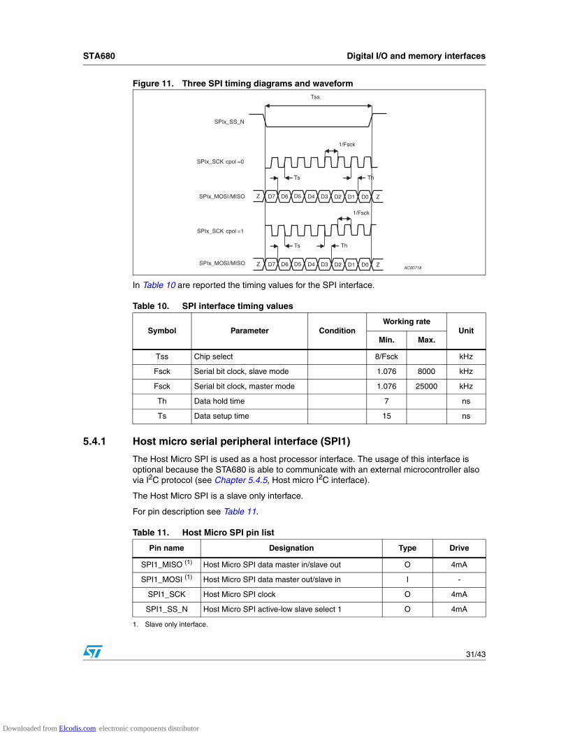
Figure 11 shows timing diagrams and waveform for the three SPI.
FSPI
Fperif8
---------------=
Downloaded from Elcodis.com electronic components distributor
STA680 Digital I/O and memory interfaces
31/43
Figure 11. Three SPI timing diagrams and waveform
In Table 10 are reported the timing values for the SPI interface.
5.4.1 Host micro serial peripheral interface (SPI1)
The Host Micro SPI is used as a host processor interface. The usage of this interface is optional because the STA680 is able to communicate with an external microcontroller also via I2C protocol (see Chapter 5.4.5, Host micro I2C interface).
The Host Micro SPI is a slave only interface.
For pin description see Table 11.
Table 10. SPI interface timing values
Symbol Parameter ConditionWorking rate
UnitMin. Max.
Tss Chip select 8/Fsck kHz
Fsck Serial bit clock, slave mode 1.076 8000 kHz
Fsck Serial bit clock, master mode 1.076 25000 kHz
Th Data hold time 7 ns
Ts Data setup time 15 ns
D6 D5 D4 D3 D2 D1 D0
SPIx_SCK cpol =0
Ts Th
1/Fsck
D7 ZZ
SPIx_SCK cpol =1
D6 D5 D4 D3 D2 D1 D0D7 ZZ
1/Fsck
Ts Th
Tss
SPIx_MOSI/MISO
SPIx_MOSI/MISO
SPIx_SS_N
AC00718
Table 11. Host Micro SPI pin list
Pin name Designation Type Drive
SPI1_MISO (1)
1. Slave only interface.
Host Micro SPI data master in/slave out O 4mA
SPI1_MOSI (1) Host Micro SPI data master out/slave in I -
SPI1_SCK Host Micro SPI clock O 4mA
SPI1_SS_N Host Micro SPI active-low slave select 1 O 4mA
Downloaded from Elcodis.com electronic components distributor

Digital I/O and memory interfaces STA680
32/43
5.4.2 Flash serial peripheral interface (SPI2)
The Flash SPI is useful for storing boot code and other configuration parameters. The minimum required capacity for this purpose is 1 Mbit.
The STA680 is SPI master only on the FLASH bus. No glue logic is necessary to connect an external Flash to the HD Radio Decoder.
In the BGA package up to 4 chips selects are available. For pin description see Table 12.
5.4.3 SD/MMC serial peripheral interface (SPI3)
The SPI SD/MMC SPI allows to connect the STA680 to a Secure Digital Card or a Multimedia Card for data storage purposes.
This interface can be configured to be master or slave and is available only in the BGA Package. For pin description see Table 13.
5.4.4 I2C interfaces
The STA680 provides two I2C interfaces that can be used to communicate with the Host Microcontroller. The first one may be used by the Host Micro in replacement of the SPI1 to control the main function of the HD Radio Decoder. The second one is an auxiliary interface and is available only in the LFBGA package option. For pin description see Table 14.
Table 12. Flash SPI pin list
Pin name Designation Type Drive
SPI2_MISO(1)
1. Slave only interface.
Flash SPI data master in/slave out I -
SPI2_MOSI(1) Flash SPI data master out/slave in O 4mA
SPI2_SCK Flash SPI clock O 4mA
SPI2_SS_N Flash SPI active-low slave select 1 O 4mA
SPI2_SS1_N Flash SPI active-low slave select 2 (2))
2. Only available in BGA package.
O 4mA
SPI2_SS2_N Flash SPI active-low slave select 3 (2) O 4mA
SPI2_SS3_N Flash SPI active-low slave select 4 (2) O 4mA
Table 13. SD/MMC SPI pin list
Pin name Designation(1)
1. Only available in BGA package
Type Drive
SPI3_MISO SD/MMC SPI data master in/slave out I/O 4mA
SPI3_MOSI SD/MMC SPI data master out/slave in I/O 4mA
SPI3_SCK SD/MMC SPI clock O 4mA
SPI3_SS_N SD/MMC SPI active-low slave select 1 O 4mA
Downloaded from Elcodis.com electronic components distributor

STA680 Digital I/O and memory interfaces
33/43
The data pins of the two I2C interfaces are open drain drivers and must have resistive pull-up conforming to Philip's IIC specification.
Figure 12 shows timing diagrams and waveform for the two I2C interfaces.
Figure 12. Timing diagrams and waveform for the two I2C interfaces
In Table 15 are reported the timing values for the I2C interface.
Table 14. Host and auxiliary I2C interface pin list
Pin name Designation Type Drive
IIC1_SCL Host Micro I2C interface serial clock line I/O 4mA
IIC1_SDA Host Micro I2C interface serial data line I/O 4mA
IIC1_DA Host Micro I2C interface data acknowledged I/O 4mA
IIC2_SCL Auxiliary I2C interface serial clock line I/O 4mA
IIC2_SDA Auxiliary I2C interface serial data line I/O 4mA
IIC2_DA Auxiliary I2C interface data acknowledged I/O 4mA
Ts,datTh,dat
Thigh
IICx_SDA
IICx_SCL
Bit 1 Bit 2 Bit n
Start Stop1/Fscl Tlow
Th,sta Th,sto
AC00719
Table 15. I2C interface timing values
Symbol Parameter ConditionStandard-mode Fast-mode
UnitMin. Max. Min. Max.
Fscl Scl clock frequency 100 400 kHz
Tlow Low period of scl clock 4.7 1.3 µs
Thigh High period of scl clock 4 0.6 µs
Th,dat Data hold time 5 µs
Ts,dat Data setup time 250 100 µs
Th,sta Hold time for start condition 4 0.6 µs
Ts,stoSetup time for stop condition
4 0.6 µs
Downloaded from Elcodis.com electronic components distributor

Digital I/O and memory interfaces STA680
34/43
5.4.5 Host micro I2C interface (I2C1)
The Host Micro I2C Interface enables the host processor to pass commands, diagnostic information, and data between the host processor and HD Radio Decoder.
The I2C1 interface is a standard I2C interface where the STA680 acts as a slave to the Host Micro and only responds to requests for information. It is also configurable by the Host Micro to work as a master to better support bi-directional flow of data and audio.
The I2C1 interface supports 7-bit addressing and 8-bit data. It can run in both standard mode (serial clock frequency up to 100 kHz) and fast mode (up to 400 kHz). The I2C device addresses are reported in Table 16.
Although not part of the IIC standard, an additional control line called IIC1_DA is provided. This line is useful for indicating when data is available and can be polled by either master or slave.
5.4.6 Auxiliary I2C interface (I2C2)
The Auxiliary I2C interface can be programmed to be a master or slave. The usage of this interface by the host processor is optional and by default it is disabled after reset.
The I2C2 interface supports 7-bit addressing and 8-bit data. It can run in both standard mode (serial clock frequency up to 100 kHz) and fast mode (up to 400 kHz). The I2C device addresses are reported in Table 17.
Although not part of the IIC standard, an additional control line called IIC1_DA is provided. This line is useful for indicating when data is available and can be polled by either master or slave.
Table 16. I2C1 interface device address
I2C1 Primary address Secondary address
Read Address 0101111b 0101101b
Write Address 0101110b 0101100b
Table 17. I2C2 interface device address
I2C2 Primary Address Secondary Address
Read Address 0101011b 0101001b
Write Address 0101010b 0101000b
Downloaded from Elcodis.com electronic components distributor
STA680 Digital I/O and memory interfaces
35/43
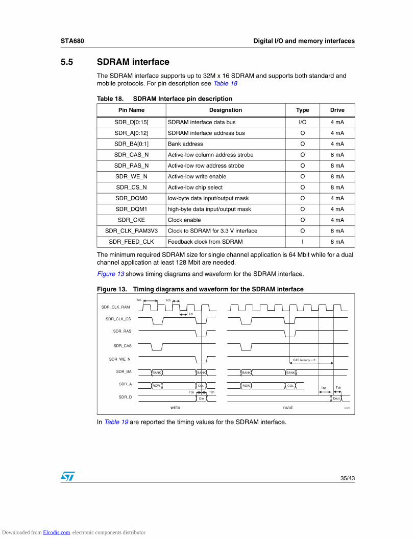
5.5 SDRAM interfaceThe SDRAM interface supports up to 32M x 16 SDRAM and supports both standard and mobile protocols. For pin description see Table 18
The minimum required SDRAM size for single channel application is 64 Mbit while for a dual channel application at least 128 Mbit are needed.
Figure 13 shows timing diagrams and waveform for the SDRAM interface.
Figure 13. Timing diagrams and waveform for the SDRAM interface
In Table 19 are reported the timing values for the SDRAM interface.
Table 18. SDRAM Interface pin description
Pin Name Designation Type Drive
SDR_D[0:15] SDRAM interface data bus I/O 4 mA
SDR_A[0:12] SDRAM interface address bus O 4 mA
SDR_BA[0:1] Bank address O 4 mA
SDR_CAS_N Active-low column address strobe O 8 mA
SDR_RAS_N Active-low row address strobe O 8 mA
SDR_WE_N Active-low write enable O 8 mA
SDR_CS_N Active-low chip select O 8 mA
SDR_DQM0 low-byte data input/output mask O 4 mA
SDR_DQM1 high-byte data input/output mask O 4 mA
SDR_CKE Clock enable O 4 mA
SDR_CLK_RAM3V3 Clock to SDRAM for 3.3 V interface O 8 mA
SDR_FEED_CLK Feedback clock from SDRAM I 8 mA
SDR_CLK_RAM
SDR_CAS
SDR_A
SDR_D
SDR_BA
SDR_WE_N
SDR_CLK_CS
SDR_RAS
ROW
BANK
COL
BANK
Din
Tds Tdh
TohTac
Dout
Tcl
TchTck
BANK BANK
ROW COL
CAS latency = 3
write read AC00720
Downloaded from Elcodis.com electronic components distributor

Digital I/O and memory interfaces STA680
36/43
Table 19. SDRAM interface timing values
Symbol Parameter Condition Min. Max. Unit
Tck SCL clock period 6.06 - ns
Tch CLK high level width 2.5 - ns
Tcl CLK low level width 2.5 - ns
Tdh Data hold time 2 - ns
Tds Data setup time 2 - ns
TacAccess time from clock (posedge)
- 5.4 ns
Toh Data out hold time 1.8 - ns
Tt Transition time - 1.2 ns
Downloaded from Elcodis.com electronic components distributor

STA680 Electrical specifications
37/43
6 Electrical specifications
6.1 Absolute maximum ratings
6.2 Thermal data
Table 20. Absolute maximum ratings
Symbol Parameter Value Unit
VDD Core supply voltage 1.3 V
VDD_GEN_IO Generic IO supply voltage 3.6 V
VDD_FSH_IO Flash IO supply voltage 3.6 V
VDD_RAM_IO SDRAM IO supply voltage 3.6 V
VDD_OSC Osc 1V8 supply voltage 1.95 V
VDD_PLL_ANA Pll analog supply voltage 2.75 V
VDD_PLL_DIG Pll digital supply voltage 1.3 V
VDD_SAF Saf core supply voltage 1.3 V
Vi Voltage on input pin -0.5 to (VDDIO* + 0.5) V
Vo Voltage on output pin -0.5 to (VDDIO* + 0.5) V
Tstg Operative storage temperature -40 to +150 °C
Tj Operative junction temperature -40 to +125 °C
Tamb Operative ambient temperature -40 to +85 °C
Table 21. Thermal data
Symbol Parameter LQFP LFBGA Unit
Rth j-amb Thermal resistance junction to ambient(1)
1. According to JEDEC specification on a 4 layers board.
30 35 °C/W
Downloaded from Elcodis.com electronic components distributor

Electrical specifications STA680
38/43
6.3 Operating conditions
Table 22. DC electrical characteristics
Symbol Parameter Test condition Min. Typ. Max. Unit
VDD Core supply voltage 1.1 1.2 1.3 V
VDD_GEN_IO Generic IO supply voltage 3.0 3.3 3.6 V
VDD_FSH_IO Flash IO supply voltage 3.0 3.3 3.6 V
VDD_RAM_IO SDRAM IO supply voltage 3.0 3.3 3.6 V
VDD_OSCOscillator analog supply voltage
1.7 1.8 1.95 V
VDD_PLL_ANA PLL analog supply voltage 1.7 1.8 2.75 V
VDD_PLL_DIG PLL digital supply voltage 1.1 1.2 1.3 V
VDD_SAF SAF supply voltage 1.1 1.2 1.3 V
IDD_1V2 Core supply current at 1.2V mA
IDD_IO IO supply current mA
Pd Power dissipation mW
IilLow level input leakage current(1) Vi = 0V 1.9 µA
IihHigh level input leakage current(1) Vi = VDD_GEN_IO(2) 1.9 µA
IlpuHigh level input leakage current on pull up(3) Vi = VDD_GEN_IO(2) 2.9 µA
IlpdLow level input leakage current on pull-down(4) Vi = 0V 10 µA
Ipu Pull-up current Vi = 0V 72 µA
Ipd Pull-down current Vi = VDD_GEN_IO(2) 72 µA
RpuEquivalent pull-up resistance(5) Vi = 0V 50 KΩ
RpdEquivalent pull-down resistance(6) Vi = VDD_GEN_IO(2) 50 KΩ
Vil Low level input voltage 3.3 supply mode -0.3 0.8 V
Vih High level input voltage 3.3 supply mode 2.0VDD_GEN_IO+0.3
V
Vhyst Input hysteresis voltage 3.3 supply mode 50 mV
Voh Output high voltage Ioh =XmA(7)VDD_RAM_IO – 0.2V
V
Vol Output low voltage Iol =XmA(7) 0.2 V
Downloaded from Elcodis.com electronic components distributor

STA680 Electrical specifications
39/43
Vesd Electrostatic discharge voltage
Human Body Model 2000 V
Machine Model 200 V
Charge device Model 500 V
Ilatchup Injection currentMaximum operating junction temperature 125 °C
100 mA
VDD_RAM_IO SDRAM IO supply voltage 3.0 3.3 3.6 V
Iil_ramLow level input leakage current(1) Vi = 0V µA
Iih_ramHigh level input leakage current(1) Vi = VDD_RAM_IO µA
Ilpu_ramHigh level input leakage current on pull up(3) Vi = VDD_RAM_IO µA
Ilpd_ramLow level input leakage current on pull-down(4) Vi = 0V µA
Ipu_ram Pull-up current Vi = 0V 44 122 µA
Ipd_ram Pull-down current Vi = VDD_RAM_IO 29 122 µA
Rpu_ramEquivalent pull-up resistance(5) Vi = 0V 29 67 KΩ
Rpd_ramEquivalent pull-down resistance(6) Vi = VDD_RAM_IO 29 103 KΩ
Vil_ram Low level input voltage 0.8 V
Vih_ram High level input voltage 2 V
Vhyst_ram Schmitt trigger hysteresis 300 800 mV
Voh_ram High level output voltage Ioh = -XmA(7)VDD_RAM_IO -
0.3V
Vol_ram Low level output voltage Iol =XmA(7) 0.3 V
1. Performed on all the input pins excluded the pull-down and pull-up ones.
2. VDD_GEN_IO may be VDD_FHS_IO or VDD_GEN_IO depending on interface considered.
3. Performed only on the Input pins with pull up.
4. Performed only on the Input pins with pull down.
5. Guaranteed by Ipu measurements.
6. Guaranteed by Ipd measurements.
7. XmA = 4mA for a BD4, 8mA for BD8 pad type.
Table 22. DC electrical characteristics (continued)
Symbol Parameter Test condition Min. Typ. Max. Unit
Downloaded from Elcodis.com electronic components distributor

Package information STA680
40/43
7 Package information
In order to meet environmental requirements, ST (also) offers these devices in ECOPACK® packages. ECOPACK® packages are lead-free. The category of second Level Interconnect is marked on the package and on the inner box label, in compliance with JEDEC Standard JESD97. The maximum ratings related to soldering conditions are also marked on the inner box label.
ECOPACK is an ST trademark. ECOPACK specifications are available at: www.st.com.
Figure 14. LQFP144 (20x20mm) mechanical data and package dimensions
OUTLINE ANDMECHANICAL DATA
DIM.mm inch
MIN. TYP. MAX. MIN. TYP. MAX.
A 1.600 0.0630
A1 0.050 0.150 0.0020 0.0059
A2 1.350 1.400 1.450 0.0531 0.0551 0.0571
b 0.170 0.220 0.270 0.0067 0.0087 0.0106
c 0.090 0.200 0.0035 0.0079
D 21.800 22.000 22.200 0.8583 0.8661 0.8740
D1 19.800 20.000 20.200 0.7795 0.7874 0.7953
D3 17.500 0.6890
E 21.800 22.000 22.200 0.8583 0.8661 0.8740
E1 19.800 20.000 20.200 0.7795 0.7874 0.7953
E3 17.500 0.6890
e 0.500 0.0197
L 0.450 0.600 0.750 0.0177 0.0236 0.0295
L1 1.000 0.0394
k 0˚(min.), 3.5˚(typ.), 7˚(max.)
ccc 0.080 0.0031
LQFP144 (20x20x1.40mm)Low profile plastic Quad Flat Package
Note 1: Exact shape of each corner is optional.
0099183 C
Downloaded from Elcodis.com electronic components distributor

STA680 Package information
41/43
Figure 15. LFBGA 168 balls (12x12x1.4 mm) mechanical data and package dimensions
OUTLINE ANDMECHANICAL DATA
DIM.mm inch
MIN. TYP. MAX. MIN. TYP. MAX.
A 1.400 0.0551
A1 0.210 0.0083
A2 0.200 0.0078
A4 0.800 0.0315
b 0.350 0.400 0.450 0.0138 0.0157 0.0177
D 11.850 12.000 12.150 0.4665 0.4724 0.4783
D1 10.400 0.4094
E 11.850 12.000 12.150 0.4665 0.4724 0.4783
E1 10.400 0.4094
e 0.800 0.0315
Z 0.800 0.0315
ddd 0.100 0.0039
eee 0.150 0.0059
fff 0.080 0.0031
LFBGA 168 ballsLow profile Fine Pitch Ball Grid Array
8123111 B
Body: 12 x 12 x 1.4mm
Downloaded from Elcodis.com electronic components distributor

Revision history STA680
42/43
8 Revision history
Table 23. Document revision history
Date Revision Changes
25-Jul-2008 1 Initial release.
Downloaded from Elcodis.com electronic components distributor

STA680
43/43
Please Read Carefully:
Information in this document is provided solely in connection with ST products. STMicroelectronics NV and its subsidiaries (“ST”) reserve theright to make changes, corrections, modifications or improvements, to this document, and the products and services described herein at anytime, without notice.
All ST products are sold pursuant to ST’s terms and conditions of sale.
Purchasers are solely responsible for the choice, selection and use of the ST products and services described herein, and ST assumes noliability whatsoever relating to the choice, selection or use of the ST products and services described herein.
No license, express or implied, by estoppel or otherwise, to any intellectual property rights is granted under this document. If any part of thisdocument refers to any third party products or services it shall not be deemed a license grant by ST for the use of such third party productsor services, or any intellectual property contained therein or considered as a warranty covering the use in any manner whatsoever of suchthird party products or services or any intellectual property contained therein.
UNLESS OTHERWISE SET FORTH IN ST’S TERMS AND CONDITIONS OF SALE ST DISCLAIMS ANY EXPRESS OR IMPLIEDWARRANTY WITH RESPECT TO THE USE AND/OR SALE OF ST PRODUCTS INCLUDING WITHOUT LIMITATION IMPLIEDWARRANTIES OF MERCHANTABILITY, FITNESS FOR A PARTICULAR PURPOSE (AND THEIR EQUIVALENTS UNDER THE LAWSOF ANY JURISDICTION), OR INFRINGEMENT OF ANY PATENT, COPYRIGHT OR OTHER INTELLECTUAL PROPERTY RIGHT.
UNLESS EXPRESSLY APPROVED IN WRITING BY AN AUTHORIZED ST REPRESENTATIVE, ST PRODUCTS ARE NOTRECOMMENDED, AUTHORIZED OR WARRANTED FOR USE IN MILITARY, AIR CRAFT, SPACE, LIFE SAVING, OR LIFE SUSTAININGAPPLICATIONS, NOR IN PRODUCTS OR SYSTEMS WHERE FAILURE OR MALFUNCTION MAY RESULT IN PERSONAL INJURY,DEATH, OR SEVERE PROPERTY OR ENVIRONMENTAL DAMAGE. ST PRODUCTS WHICH ARE NOT SPECIFIED AS "AUTOMOTIVEGRADE" MAY ONLY BE USED IN AUTOMOTIVE APPLICATIONS AT USER’S OWN RISK.
Resale of ST products with provisions different from the statements and/or technical features set forth in this document shall immediately voidany warranty granted by ST for the ST product or service described herein and shall not create or extend in any manner whatsoever, anyliability of ST.
ST and the ST logo are trademarks or registered trademarks of ST in various countries.
Information in this document supersedes and replaces all information previously supplied.
The ST logo is a registered trademark of STMicroelectronics. All other names are the property of their respective owners.
© 2008 STMicroelectronics - All rights reserved
STMicroelectronics group of companies
Australia - Belgium - Brazil - Canada - China - Czech Republic - Finland - France - Germany - Hong Kong - India - Israel - Italy - Japan - Malaysia - Malta - Morocco - Singapore - Spain - Sweden - Switzerland - United Kingdom - United States of America
www.st.com
Downloaded from Elcodis.com electronic components distributor