© digital integrated circuits 2nd and f. brewer 2003 design methodologies design methodology
Post on 21-Dec-2015
217 views
TRANSCRIPT
© Digital Integrated Circuits2nd and F. Brewer 2003 Design Methodologies
Design Design MethodologyMethodology

© Digital Integrated Circuits2nd and F. Brewer 2003 Design Methodologies
The Design Productivity ChallengeThe Design Productivity Challenge
Source: ITRS’97
A growing gap between design complexity and design productivity
58%/Yr. compound
Complexity growth rate
21%/Yr. compound
Productivity growth rate
19
81
Logic
Tra
nsi
stors
per
Chip
(K
)
Pro
duct
ivit
y (
Tra
ns.
/Sta
ff-M
onth
)
100
1,000
10,000
100,000
1,000,000
10,000,000
100
1,000 10,000
100,000
1,000,000
10,000,000
100,000,000
10
19
85
19
89
19
93
19
97
20
01
20
05
20
09
© Digital Integrated Circuits2nd and F. Brewer 2003 Design Methodologies
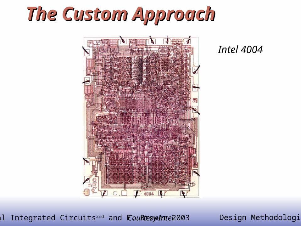
The Custom Approach The Custom Approach
Intel 4004
Courtesy Intel

© Digital Integrated Circuits2nd and F. Brewer 2003 Design Methodologies
Transition to Automation and Regular StructuresTransition to Automation and Regular Structures
Intel 4004 (‘71)Intel 4004 (‘71)Intel 8080Intel 8080 Intel 8085Intel 8085
Intel 80286Intel 80286 Intel 80486Intel 80486Courtesy Intel

© Digital Integrated Circuits2nd and F. Brewer 2003 Design Methodologies
Automating DesignAutomating Design
Exploitation By Algorithms Regular Structures Logic Synthesis Regularization of Connection
Floorplanning (Localization of function) System Level Performance/Power/Cost Allocation of Physical Resources
Communication/Interconnect Hierarchy based on Sensitivity to Latency Wires to Link Protocols

© Digital Integrated Circuits2nd and F. Brewer 2003 Design Methodologies
A System-on-a-Chip: ExampleA System-on-a-Chip: Example
Courtesy: Philips
© Digital Integrated Circuits2nd and F. Brewer 2003 Design Methodologies
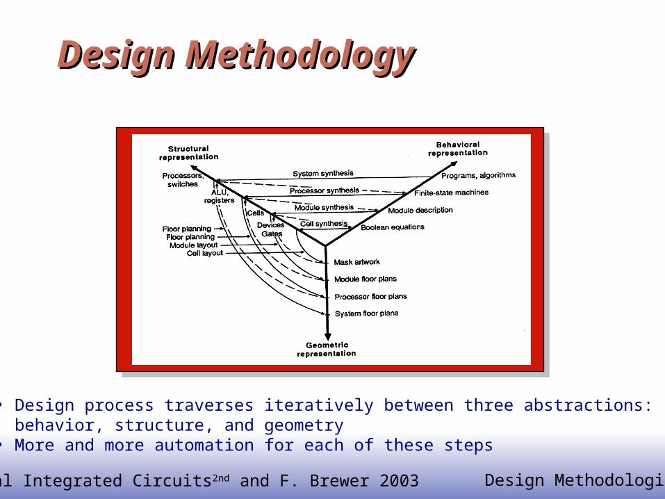
Design MethodologyDesign Methodology
• Design process traverses iteratively between three abstractions: behavior, structure, and geometry• More and more automation for each of these steps

© Digital Integrated Circuits2nd and F. Brewer 2003 Design Methodologies
FloorplanningFloorplanning
A Protocol Processor for Wireless
© Digital Integrated Circuits2nd and F. Brewer 2003 Design Methodologies
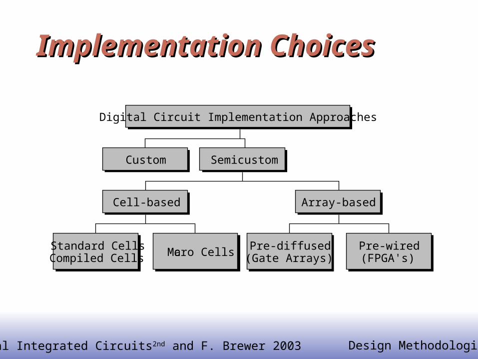
Implementation ChoicesImplementation Choices
Custom
Standard CellsCompiled Cells Macro Cells
Cell-based
Pre-diffused(Gate Arrays)
Pre-wired(FPGA's)
Array-based
Semicustom
Digital Circuit Implementation Approaches
© Digital Integrated Circuits2nd and F. Brewer 2003 Design Methodologies
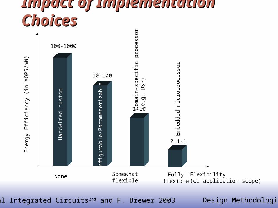
Impact of Implementation ChoicesImpact of Implementation ChoicesE
nerg
y E
ffic
ienc
y (i
n M
OP
S/m
W)
Flexibility(or application scope)
0.1-1
1-10
10-100
100-1000
None Fullyflexible
Somewhatflexible
Har
dwire
d cu
stom
Con
figur
able
/Par
amet
eriz
able
Dom
ain
-spe
cific
pro
cess
or(e
.g.
DS
P)
Em
bedd
ed m
icro
proc
ess
or

© Digital Integrated Circuits2nd and F. Brewer 2003 Design Methodologies
Implementation StrategiesImplementation Strategies
PLA Technology confined in cell macros (tiling)
Cell based logic Technology confined to cells (area) Both 1-d and 2-d solutions
Transistor Arrays (Gate arrays) Technology confined to layers (Below M1
fixed)

© Digital Integrated Circuits2nd and F. Brewer 2003 Design Methodologies
PLA: Programmable Logic ArrayPLA: Programmable Logic Array
x0 x1 x2
ANDplane
x0x1
x2
Product terms
ORplane
f0 f1
© Digital Integrated Circuits2nd and F. Brewer 2003 Design Methodologies
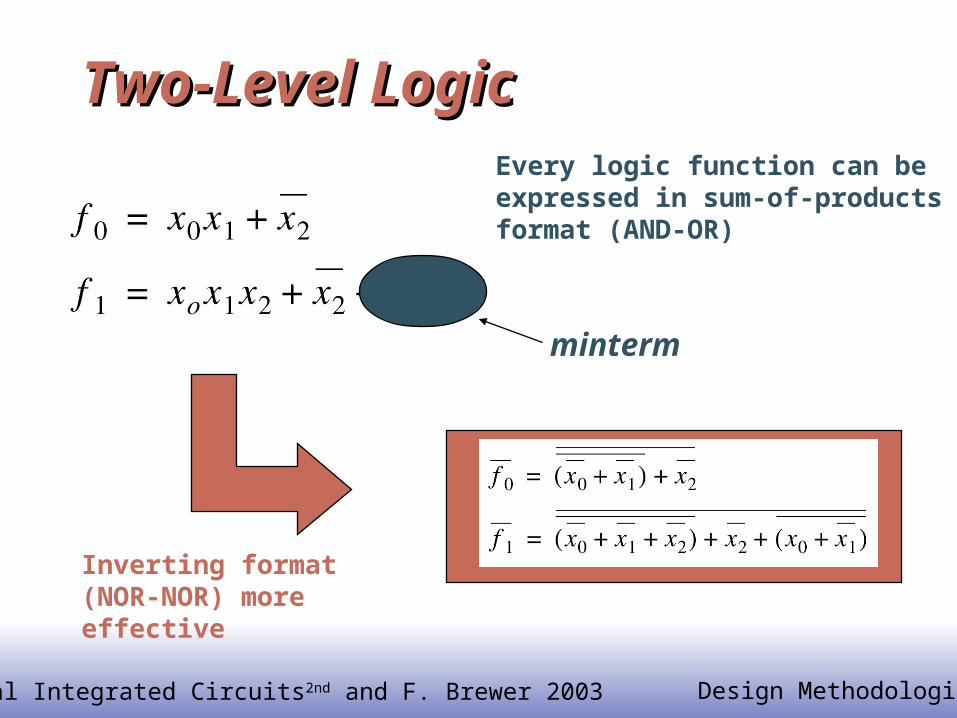
Two-Level LogicTwo-Level Logic
Inverting format (NOR-NOR) more effective
Every logic function can beexpressed in sum-of-productsformat (AND-OR)
minterm

© Digital Integrated Circuits2nd and F. Brewer 2003 Design Methodologies
PLA Layout – Exploiting RegularityPLA Layout – Exploiting Regularity
f0 f1x0 x0 x1 x1 x2 x2
Pull-up devices Pull-up devices
VDD GNDAnd-Plane Or-Plane

© Digital Integrated Circuits2nd and F. Brewer 2003 Design Methodologies
Breathing Some New Life in PLAsBreathing Some New Life in PLAsRiver PLAs A cascade of multiple-output PLAs. Adjacent PLAs are connected via river routing.
PRE-CHARGE
PR
E-
CH
AR
GE
PRE-CHARGE
PR
E-C
HA
RG
E
BUFFER
BUFFER
BU
FF
ER
BU
FF
ER
PRE-CHARGE
PR
E-C
HA
RG
E
BUFFER
BU
FF
ER
PRE-CHARGE
PR
E-
CH
AR
GE
BUFFERB
UF
FE
R
• No placement and routing needed. • Output buffers and the input buffers
of the next stage are shared.
Courtesy B. Brayton
© Digital Integrated Circuits2nd and F. Brewer 2003 Design Methodologies
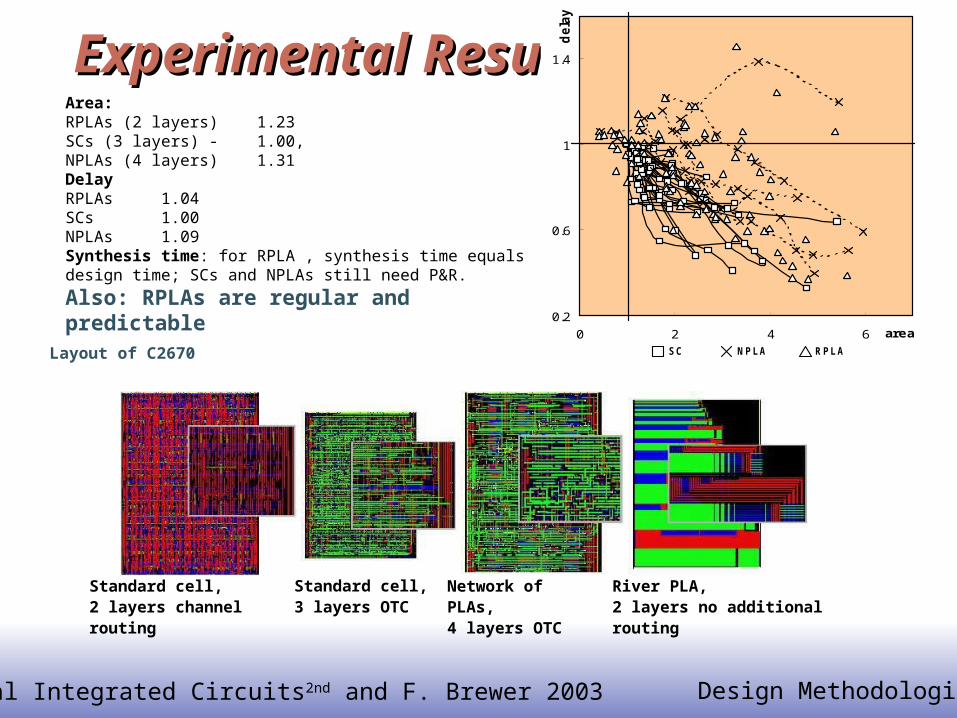
Experimental ResultsExperimental Results
Layout of C2670
Network of PLAs, 4 layers OTC
River PLA,2 layers no additional routing
Standard cell, 2 layers channel routing
Standard cell,3 layers OTC
0.2
0.6
1
1.4
0 2 4 6 area
dela
y
SC N PLA R PLA
Area: RPLAs (2 layers) 1.23 SCs (3 layers) - 1.00, NPLAs (4 layers) 1.31 DelayRPLAs 1.04SCs 1.00 NPLAs 1.09 Synthesis time: for RPLA , synthesis time equals design time; SCs and NPLAs still need P&R.
Also: RPLAs are regular and predictable

© Digital Integrated Circuits2nd and F. Brewer 2003 Design Methodologies
2-d Cell Based: “Hard” Modules2-d Cell Based: “Hard” Modules
25632 (or 8192 bit) SRAMGenerated by hard-macro module generator

© Digital Integrated Circuits2nd and F. Brewer 2003 Design Methodologies
1-d Cell-based Design (standard cells)1-d Cell-based Design (standard cells)
Routing channel requirements arereduced by presenceof more interconnectlayers
Functionalmodule
(RAM,multiplier,)
Routingchannel
Logic cellFeedthrough cell
Rows ofcells

© Digital Integrated Circuits2nd and F. Brewer 2003 Design Methodologies
Standard Cell — ExampleStandard Cell — Example
[Brodersen92]

© Digital Integrated Circuits2nd and F. Brewer 2003 Design Methodologies
Standard Cell – The New GenerationStandard Cell – The New Generation
Cell-structurehidden underinterconnect layers
© Digital Integrated Circuits2nd and F. Brewer 2003 Design Methodologies
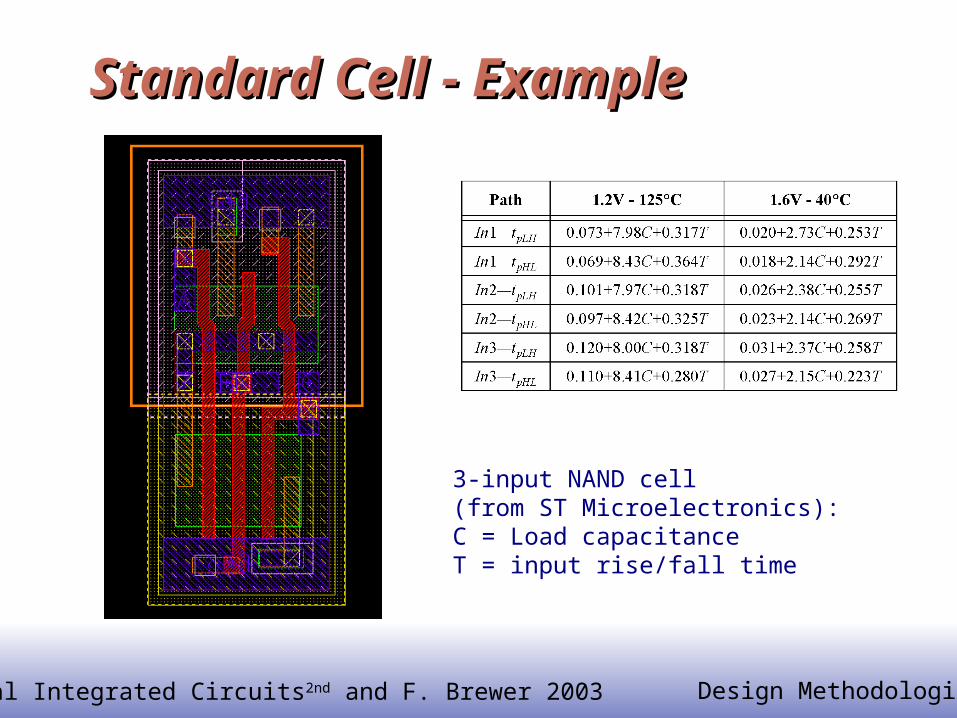
Standard Cell - ExampleStandard Cell - Example
3-input NAND cell(from ST Microelectronics):C = Load capacitanceT = input rise/fall time

© Digital Integrated Circuits2nd and F. Brewer 2003 Design Methodologies
““Soft” MacroModulesSoft” MacroModules
Synopsys DesignCompiler

© Digital Integrated Circuits2nd and F. Brewer 2003 Design Methodologies
The “Design Closure” ProblemThe “Design Closure” Problem
Courtesy Synopsys
Iterative Removal of Timing Violations (white lines)

© Digital Integrated Circuits2nd and F. Brewer 2003 Design Methodologies
Gate Array — Sea-of-gatesGate Array — Sea-of-gates
rows of
cells
routing channel
uncommitted
VDD
GND
polysilicon
metal
possiblecontact
In1 In2 In3 In4
Out
UncommitedCell
CommittedCell(4-input NOR)

© Digital Integrated Circuits2nd and F. Brewer 2003 Design Methodologies
Sea-of-gate Primitive CellsSea-of-gate Primitive Cells
NMOS
PMOS
Oxide-isolation
PMOS
NMOS
NMOS
Using oxide-isolation Using gate-isolation

© Digital Integrated Circuits2nd and F. Brewer 2003 Design Methodologies
Sea-of-gatesSea-of-gates
Random Logic
MemorySubsystem
LSI Logic LEA300K(0.6 m CMOS)
Courtesy LSI Logic

© Digital Integrated Circuits2nd and F. Brewer 2003 Design Methodologies
The return of gate arrays?The return of gate arrays?
metal-5 metal-6
Via-programmable cross-point
programmable via
Via programmable gate array(VPGA)
[Pileggi02]
Exploits regularity of interconnect

© Digital Integrated Circuits2nd and F. Brewer 2003 Design Methodologies
Pre-wired Arrays:Pre-wired Arrays:Classification of prewired arrays (or field-programmable devices): Based on Programming Technique
Fuse-based (program-once) Non-volatile EPROM based RAM based
Programmable Logic Style Array-Based Look-up Table
Programmable Interconnect Style Channel-routing Mesh networks

© Digital Integrated Circuits2nd and F. Brewer 2003 Design Methodologies
Fuse-Based FPGAFuse-Based FPGA
antifuse polysilicon ONO dielectric
n+ antifuse diffusion
2
From Smith’97
Open by default, closed by applying current pulse

© Digital Integrated Circuits2nd and F. Brewer 2003 Design Methodologies
Array-Based Programmable LogicArray-Based Programmable Logic
PLA (flexible – sizing) PROM (dense) PAL (uniform load)
I 5 I 4
O0
I 3 I 2 I 1 I 0
O1O2O3
Programmable AND array
ProgrammableOR array I5 I4
O0
I3 I2 I1 I0
O1O2O3
Programmable AND array
Fixed OR array
Indicates programmable connection
Indicates fixed connection
O0
I3 I2 I1 I0
O1O2O3
Fixed AND array
ProgrammableOR array
© Digital Integrated Circuits2nd and F. Brewer 2003 Design Methodologies
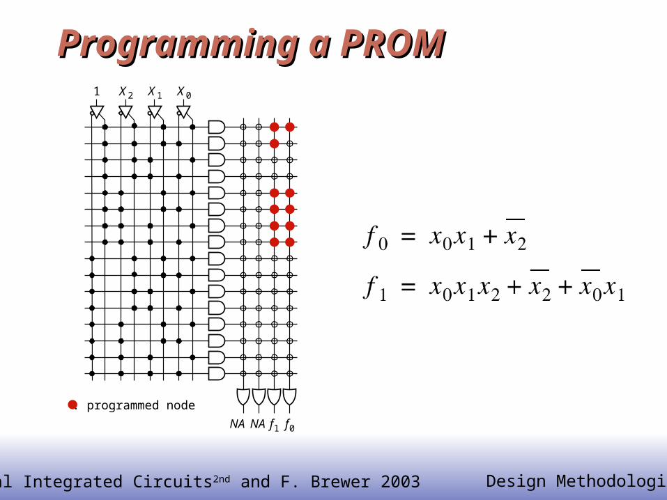
Programming a PROMProgramming a PROM
f0
1 X 2 X 1 X 0
f1NANA
: programmed node

© Digital Integrated Circuits2nd and F. Brewer 2003 Design Methodologies
2-input mux 2-input mux as programmable logic blockas programmable logic block
FA 0
B
S
1
Configuration
A B S F=
0 0 0 00 X 1 X0 Y 1 Y0 Y X XYX 0 YY 0 XY 1 X X +Y 1 0 X1 0 Y1 1 1 1
XYX Y
XY
© Digital Integrated Circuits2nd and F. Brewer 2003 Design Methodologies
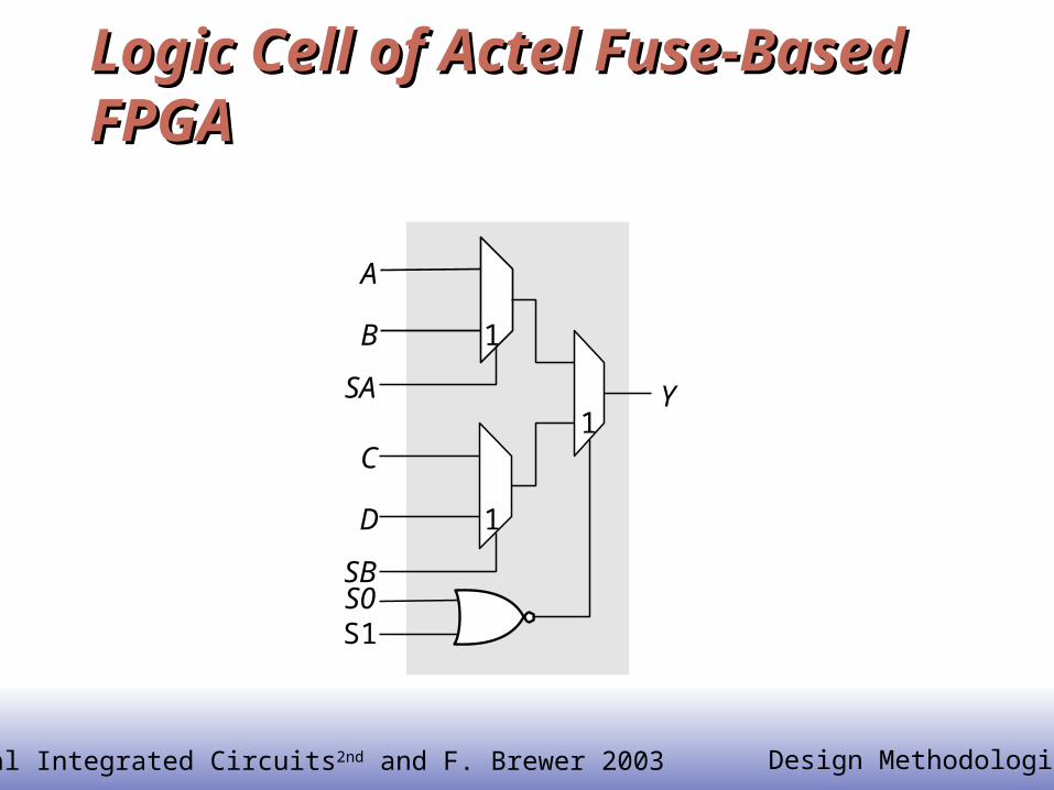
Logic Cell of Actel Fuse-Based FPGALogic Cell of Actel Fuse-Based FPGA
A
B
SA Y
C
D
SB
1
S1S0
1
1

© Digital Integrated Circuits2nd and F. Brewer 2003 Design Methodologies
LUT-Based Logic CellLUT-Based Logic Cell
Courtesy Xilinx
D4
C1....C4
clock
D3
D2
D1
F4
F3
F2
F1
Logicfunction
F
Logicfunction
H
Logicfunction
G
DinF’G’H’
H1
4
DinF’G’H’
G’H’
H2 H0 EC
H’F’
S/Rcontrol
S/Rcontrol
Multiplexer Controlledby Configuration Program
D
Y1
1
EC
QSD YQ
Bypass
X
XQBypass
RD
D
EC
QSD
RD
Xilinx 4000 Series

© Digital Integrated Circuits2nd and F. Brewer 2003 Design Methodologies
Array-Based Programmable WiringArray-Based Programmable Wiring
Input/output pinProgrammed interconnection
InterconnectPoint
Horizontaltracks
Vertical tracks
Cell
M

© Digital Integrated Circuits2nd and F. Brewer 2003 Design Methodologies
Mesh-based Interconnect NetworkMesh-based Interconnect NetworkSwitch Box
Connect Box
InterconnectPoint
Courtesy Dehon and Wawrzyniek

© Digital Integrated Circuits2nd and F. Brewer 2003 Design Methodologies
Transistor Implementation of MeshTransistor Implementation of Mesh
Courtesy Dehon and Wawrzyniek

© Digital Integrated Circuits2nd and F. Brewer 2003 Design Methodologies
Hierarchical Mesh NetworkHierarchical Mesh Network
Use overlayed meshto support longer connections
Reduced fanout and reduced resistance
Courtesy Dehon and Wawrzyniek

© Digital Integrated Circuits2nd and F. Brewer 2003 Design Methodologies
Altera MAXAltera MAX
From Smith97

© Digital Integrated Circuits2nd and F. Brewer 2003 Design Methodologies
Altera MAX Interconnect ArchitectureAltera MAX Interconnect Architecture
LAB2
PIA
LAB1
LAB6
tPIA
tPIA
row channelcolumn channel
LAB
Courtesy Altera
Array-based(MAX 3000-7000)
Mesh-based(MAX 9000)
© Digital Integrated Circuits2nd and F. Brewer 2003 Design Methodologies
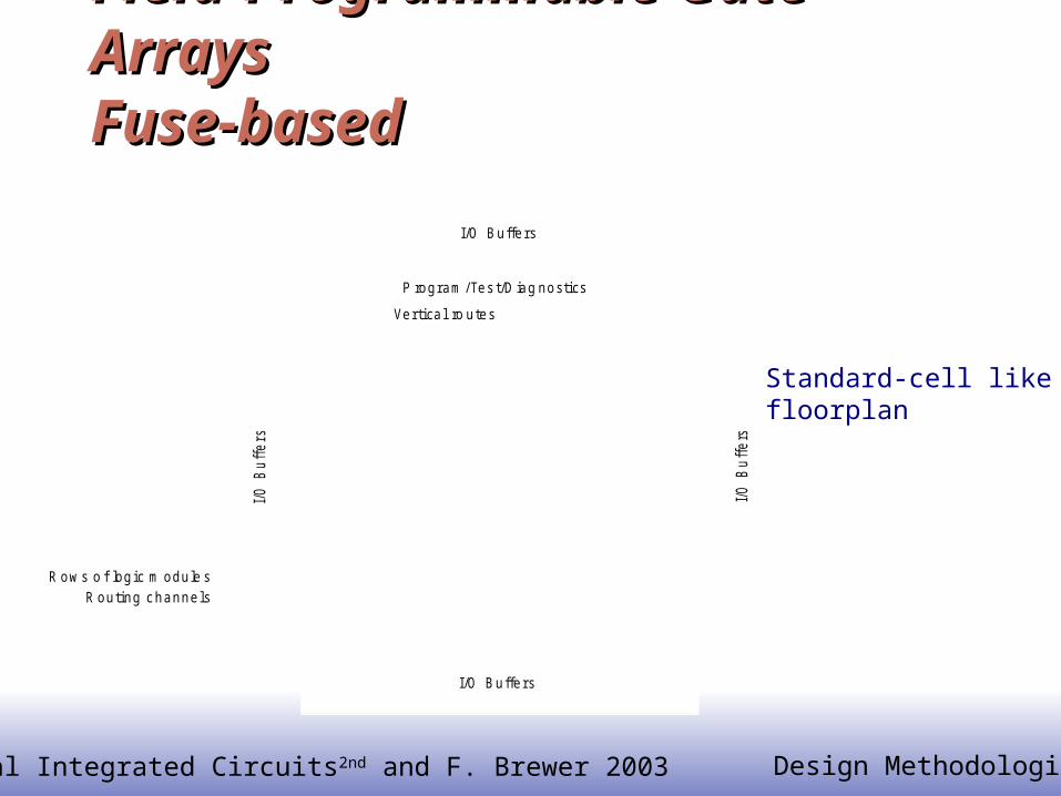
Field-Programmable Gate ArraysField-Programmable Gate ArraysFuse-basedFuse-based
I/O Buffers
P rogram/Test/Diag nostics
I/O Buffers
I/O B
uffe
rs
I/O B
uffe
rs
Vertical ro utes
Rows o f logic m odule s
Routing channels
Standard-cell likefloorplan

© Digital Integrated Circuits2nd and F. Brewer 2003 Design Methodologies
Xilinx 4000 Interconnect ArchitectureXilinx 4000 Interconnect Architecture
2
12
8
4
3
2
3
CLB
8 4 8 4
Quad
Single
Double
Long
DirectConnect
DirectConnect
Quad Long GlobalClock
Long Double Single GlobalClock
CarryChain
Long
12 4 4
Courtesy Xilinx
© Digital Integrated Circuits2nd and F. Brewer 2003 Design Methodologies
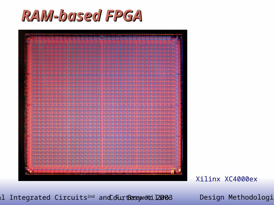
RAM-based FPGA RAM-based FPGA
Xilinx XC4000ex
Courtesy Xilinx

© Digital Integrated Circuits2nd and F. Brewer 2003 Design Methodologies
Design at a crossroadDesign at a crossroad
System-on-a-ChipSystem-on-a-Chip
RAM
500 k Gates FPGA+ 1 Gbit DRAMPreprocessing
Multi-
SpectralImager
Csystem+2 GbitDRAMRecog-
nition
Ana
log
64 SIMD ProcessorArray + SRAM
Image Conditioning100 GOPS
Embedded applications: cost, performance, and energy are the issues!
DSP and control intensive Mixed-mode Software design is crucial

© Digital Integrated Circuits2nd and F. Brewer 2003 Design Methodologies
Addressing the Design Complexity IssueAddressing the Design Complexity IssueArchitecture ReuseArchitecture Reuse
Reuse comes in generationsGeneration Reuse element Status
1st Standard cells Well established
2nd IP blocks Established- marginal
3rd Architecture Need for Standards
4th IC Marketing Hype
5th Software Current Practice
© Digital Integrated Circuits2nd and F. Brewer 2003 Design Methodologies
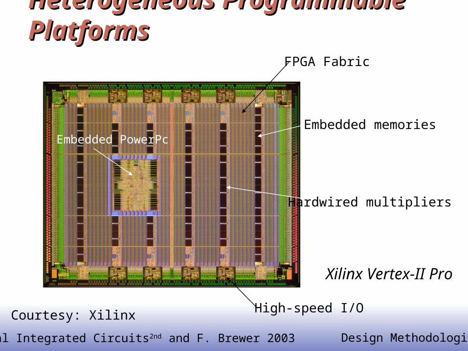
Heterogeneous Programmable PlatformsHeterogeneous Programmable Platforms
Xilinx Vertex-II Pro
Courtesy: Xilinx High-speed I/O
Embedded PowerPcEmbedded memories
Hardwired multipliers
FPGA Fabric

© Digital Integrated Circuits2nd and F. Brewer 2003 Design Methodologies
SummarySummary
Design Choice forced by System Tradeoffs Deep Sub-micron Challenges
Regularity (Design flexibility at smallest scales) Power consumption! Interconnection Parasitics Nanoscopic Devices/Modules
New circuit solutions are bound to emerge
Who can afford design in the years to come?