˘ ˇ - analog, embedded processing, semiconductor … devices are optimized for balanced multipoint...
TRANSCRIPT
SLLS447C − OCTOBER 2000 − REVISED AUGUST 2008
1POST OFFICE BOX 655303 • DALLAS, TEXAS 75265
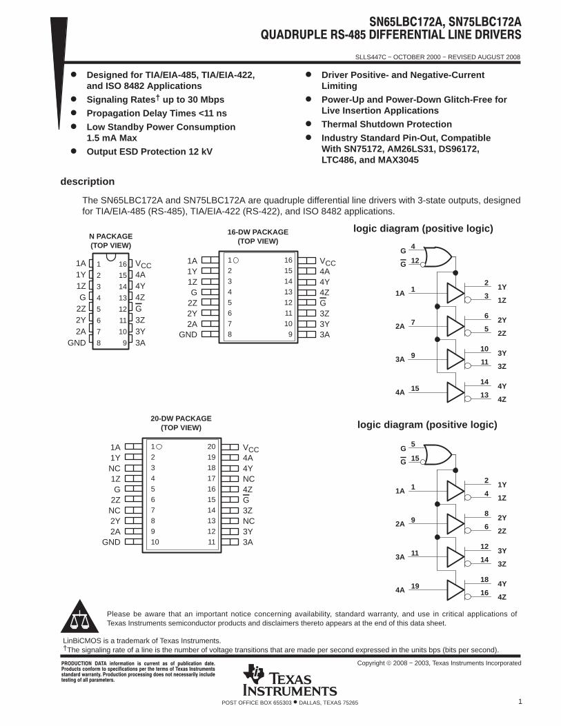
Designed for TIA/EIA-485, TIA/EIA-422,and ISO 8482 Applications
Signaling Rates † up to 30 Mbps
Propagation Delay Times <11 ns
Low Standby Power Consumption1.5 mA Max
Output ESD Protection 12 kV
Driver Positive- and Negative-CurrentLimiting
Power-Up and Power-Down Glitch-Free forLive Insertion Applications
Thermal Shutdown Protection
Industry Standard Pin-Out, CompatibleWith SN75172, AM26LS31, DS96172,LTC486, and MAX3045
description
The SN65LBC172A and SN75LBC172A are quadruple differential line drivers with 3-state outputs, designedfor TIA/EIA-485 (RS-485), TIA/EIA-422 (RS-422), and ISO 8482 applications.
1
2
3
4
5
6
7
8
16
15
14
13
12
11
10
9
1A1Y1ZG
2Z2Y2A
GND
VCC4A4Y4ZG3Z3Y3A
N PACKAGE(TOP VIEW)
logic diagram (positive logic)
4Z
4Y
3Z
3Y
2Z
2Y
1Z
1Y
4A
3A
2A
1A 1
7
9
15
G
G 12
4
2
3
6
5
10
11
14
13
4Z
4Y
3Z
3Y
2Z
2Y
1Z
1Y
4A
3A
2A
1A 1
9
11
19
G
G 15
5
2
4
8
6
12
14
18
16
logic diagram (positive logic)
1
2
3
4
5
6
78
16
15
14
13
12
11
109
1A1Y1ZG
2Z2Y2A
GND
VCC4A4Y4ZG3Z3Y3A
16-DW PACKAGE(TOP VIEW)
1
2
3
4
5
6
78
9
10
20
19
18
17
16
15
1413
12
11
1A1YNC1ZG
2ZNC2Y2A
GND
VCC4A4YNC4ZG3ZNC3Y3A
20-DW PACKAGE(TOP VIEW)
Copyright 2008 − 2003, Texas Instruments Incorporated !"# $ %&'# "$ (&)*%"# +"#',+&%#$ %! # $('%%"#$ (' #-' #'!$ '."$ $#&!'#$$#"+"+ /""#0, +&%# (%'$$1 +'$ # '%'$$"*0 %*&+'#'$#1 "** (""!'#'$,
Please be aware that an important notice concerning availability, standard warranty, and use in critical applications ofTexas Instruments semiconductor products and disclaimers thereto appears at the end of this data sheet.
LinBiCMOS is a trademark of Texas Instruments.†The signaling rate of a line is the number of voltage transitions that are made per second expressed in the units bps (bits per second).
SLLS447C − OCTOBER 2000 − REVISED AUGUST 2008
2 POST OFFICE BOX 655303 • DALLAS, TEXAS 75265
description (continued)
These devices are optimized for balanced multipoint bus transmission at signalling rates up to 30 million bitsper second. The transmission media may be printed-circuit board traces, backplanes, or cables. The ultimaterate and distance of data transfer is dependent upon the attenuation characteristics of the media and the noisecoupling to the environment.
Each driver features current limiting and thermal-shutdown circuitry making it suitable for high-speed mulitpointdata transmission applications in noisy environments. These devices are designed using LinBiCMOS,facilitating low power consumption and robustness.
The G and G inputs provide driver enable control using either positive or negative logic. When disabled orpowered off, the driver outputs present a high-impedance to the bus for reduced system loading.
The SN75LBC172A is characterized for operation over the temperature range of 0°C to 70°C. TheSN65LBC172A is characterized over the temperature range from –40°C to 85°C.
AVAILABLE OPTIONS
PACKAGE
TA16-PIN PLASTIC
SMALL OUTLINE †
(JEDEC MS-013)
20-PIN PLASTICSMALL OUTLINE †
(JEDEC MS-013)
16-PIN PLASTICTHROUGH-HOLE(JEDEC MS-001)
0°C to 70°CSN75LBC172A16DW SN75LBC172ADW SN75LBC172AN
0°C to 70°CMarked as 75LBC172A
−40°C to 85°CSN65LBC172A16DW SN65LBC172ADW SN65LBC172AN
−40°C to 85°CMarked as 65LBC172A
† Add R suffix for taped and reeled version.
FUNCTION TABLE(EACH DRIVER)
INPUT ENABLES OUTPUTS
A G G Y Z
L H X L H
L X L L H
H H X H L
H X L H L
OPEN H X H L
OPEN X L H L
H OPEN X H L
L OPEN X L H
X L H Z Z
X L OPEN Z Z
H = high level, L = low level, X = irrelevant,Z = high impedance (off)
SLLS447C − OCTOBER 2000 − REVISED AUGUST 2008
3POST OFFICE BOX 655303 • DALLAS, TEXAS 75265
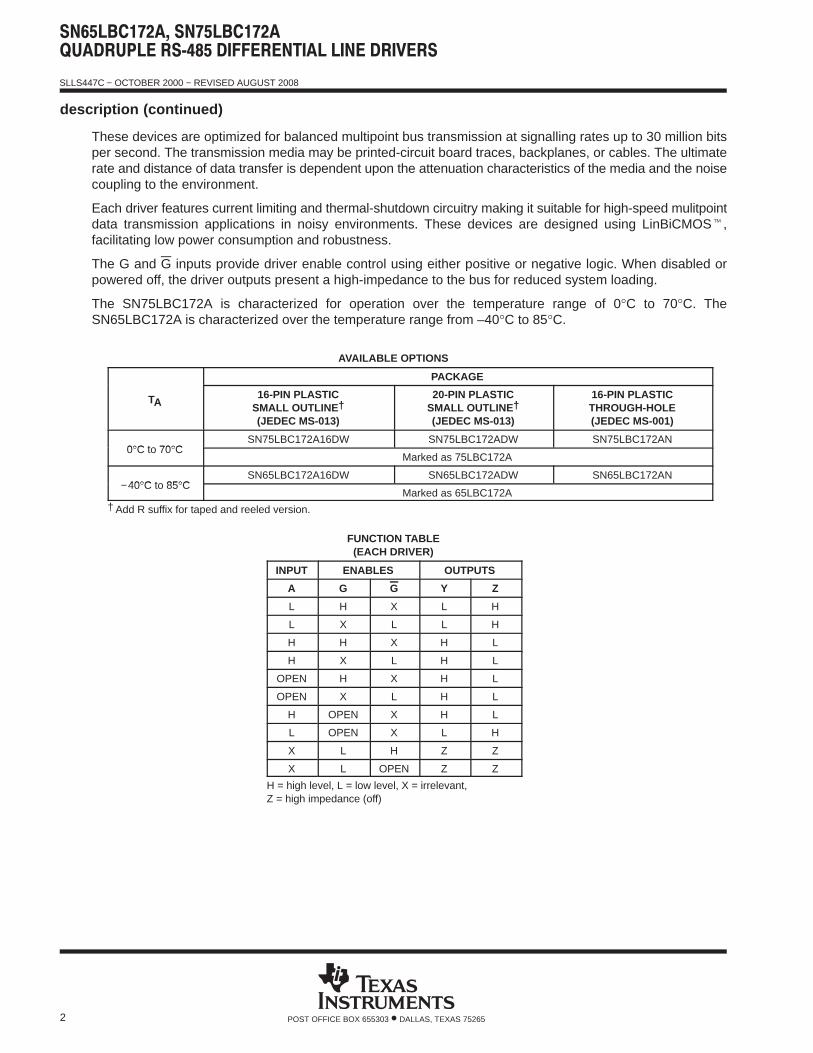
equivalent input and output schematic diagrams
VCC
A, G, or G Input
1 kΩ
9 V
Input
100 kΩ
VCC
Output
16 V
Y or Z Output
16 V
20 V
17 V
16 V
16 V
absolute maximum ratings †
Supply voltage range, VCC (see Note 1) −0.3 V to 6 V. . . . . . . . . . . . . . . . . . . . . . . . . . . . . . . . . . . . . . . . . . . . . . Output voltage range, VO, at any bus (steady state) −10 V to 15 V. . . . . . . . . . . . . . . . . . . . . . . . . . . . . . . . . . . . . . Output voltage range, VO, at any bus (transient pulse through 100 Ω, see Figure 8) −30 V to 30 V. . . . . . . . . . . Input voltage range, VI, at any A, G, or G terminal −0.5 V to VCC + 0.5 V. . . . . . . . . . . . . . . . . . . . . . . . . . . . . . . . Electrostatic discharge: Human body model (see Note 2) Y, Z, and GND 12 kV. . . . . . . . . . . . . . . . . . . . .
All pins 5 kV. . . . . . . . . . . . . . . . . . . . . . . . . . . . . Charged-device model (see Note 3) All pins 1 kV. . . . . . . . . . . . . . . . . . . . . . . . . . . . .
Storage temperature range, Tstg −65°C to 150°C. . . . . . . . . . . . . . . . . . . . . . . . . . . . . . . . . . . . . . . . . . . . . . . . . . . Continuous power dissipation See Dissipation Rating Table. . . . . . . . . . . . . . . . . . . . . . . . . . . . . . . . . . . . . . . . . Lead temperature 1,6 mm (1/16 inch) from case for 10 seconds 260°C. . . . . . . . . . . . . . . . . . . . . . . . . . . . . . .
† Stresses beyond those listed under “absolute maximum ratings” may cause permanent damage to the device. These are stress ratings only, andfunctional operation of the device at these or any other conditions beyond those indicated under “recommended operating conditions” is notimplied. Exposure to absolute-maximum-rated conditions for extended periods may affect device reliability.
NOTES: 1. All voltage values, except differential I/O bus voltages, are with respect to GND.2. Tested in accordance with JEDEC standard 22, Test Method A114−A.3. Tested in accordance with JEDEC standard 22, Test Method C101.
DISSIPATION RATING TABLE
PACKAGEJEDECBOARDMODEL
TA ≤ 25°CPOWER RATING
DERATING FACTOR‡
ABOVE TA = 25°CTA = 70°C
POWER RATINGTA = 85°C
POWER RATING
16-PIN DWLow K 1200 mW 9.6 mW/°C 769 mW 625 mW
16-PIN DWHigh K 2240 mW 17.9 mW/°C 1434 mW 1165 mW
20-PIN DWLow K 1483 mW 11.86 mW/°C 949 mW 771 mW
20-PIN DWHigh K 2753 mW 22 mW/°C 1762 mW 1432 mW
16-PIN N Low K 1150 mW 9.2 mW/°C 736 mW 598 mW‡ This is the inverse of the junction-to-ambient thermal resistance when board-mounted with no air flow.
SLLS447C − OCTOBER 2000 − REVISED AUGUST 2008
4 POST OFFICE BOX 655303 • DALLAS, TEXAS 75265
recommended operating conditions
MIN NOM MAX UNIT
Supply voltage, VCC 4.75 5 5.25 V
Voltage at any bus terminal Y, Z −7 12 V
High-level input voltage, VIHA, G, G
2 VCCV
Low-level input voltage, VILA, G, G
0 0.8V
Output current −60 60 mA
Operating free-air temperature, TASN75LBC172A 0 70
°COperating free-air temperature, TA SN65LBC172A −40 85°C
electrical characteristics over recommended operating conditions
PARAMETER TEST CONDITIONS MIN TYP† MAX UNIT
VIK Input clamp voltage II = −18 mA −1.5 −0.77 V
VO Open-circuit output voltage Y or Z, No load 0 VCC V
Steady-state differential output voltageNo load (open circuit) 3 VCC
VOD(SS)Steady-state differential output voltage
‡ RL = 54 Ω, see Figure 1 1 1.6 2.5 VVOD(SS)Steady-state differential output voltagemagnitude‡ RL = 54 Ω, see Figure 1 1 1.6 2.5 VVOD(SS) magnitude‡
With common-mode loading, see Figure 2 1 1.6 2.5
Vmagnitude
With common-mode loading, see Figure 2 1 1.6 2.5
∆VOD(SS)Change in steady-state differential outputvoltage between logic states
See Figure 1 −0.1 0.1 V
VOC(SS)Steady-state common-mode outputvoltage
See Figure 3 2 2.4 2.8 V
∆VOC(SS)Change in steady-state common-modeoutput voltage between logic states
See Figure 3 −0.02 0.02 V
II Input current A, G, G −50 50 µA
IOS Short-circuit output currentVI = 0 V
−200 200 mAIOS Short-circuit output current
VTEST = −7 V to 12 V,VI = VCC
−200 200 mA
IOZ High-impedance-state output currentVTEST = −7 V to 12 V,See Figure 7 G at 0 V, G at VCC −50 50
AIO(OFF) Output current with power off
See Figure 7VCC = 0 V −10 10
µA
ICC Supply currentVI = 0 V or VCC, All drivers enabled 23
mAICC Supply currentVI = 0 V or VCC,No load All drivers disabled 1.5
mA
† All typical values are at VCC = 5 V and 25°C.‡ The minimum VOD may not fully comply with TIA/EIA-485-A at operating temperatures below 0°C. System designers should take the possibly
of lower output signal into account in determining the maximum signal transmission distance.
SLLS447C − OCTOBER 2000 − REVISED AUGUST 2008
5POST OFFICE BOX 655303 • DALLAS, TEXAS 75265
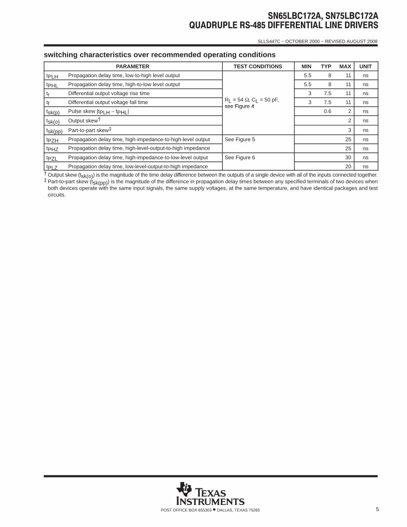
switching characteristics over recommended operating conditions
PARAMETER TEST CONDITIONS MIN TYP MAX UNIT
tPLH Propagation delay time, low-to-high level output 5.5 8 11 ns
tPHL Propagation delay time, high-to-low level output 5.5 8 11 ns
tr Differential output voltage rise timeR = 54 , C = 50 pF,
3 7.5 11 ns
tf Differential output voltage fall time RL = 54 Ω, CL = 50 pF, see Figure 4
3 7.5 11 ns
tsk(p) Pulse skew |tPLH – tPHL|see Figure 4
0.6 2 ns
tsk(o) Output skew† 2 ns
tsk(pp) Part-to-part skew‡ 3 ns
tPZH Propagation delay time, high-impedance-to-high-level output See Figure 5 25 ns
tPHZ Propagation delay time, high-level-output-to-high impedance 25 ns
tPZL Propagation delay time, high-impedance-to-low-level output See Figure 6 30 ns
tPLZ Propagation delay time, low-level-output-to-high impedance 20 ns† Output skew (tsk(o)) is the magnitude of the time delay difference between the outputs of a single device with all of the inputs connected together.‡ Part-to-part skew (tsk(pp)) is the magnitude of the difference in propagation delay times between any specified terminals of two devices when
both devices operate with the same input signals, the same supply voltages, at the same temperature, and have identical packages and testcircuits.
SLLS447C − OCTOBER 2000 − REVISED AUGUST 2008
6 POST OFFICE BOX 655303 • DALLAS, TEXAS 75265
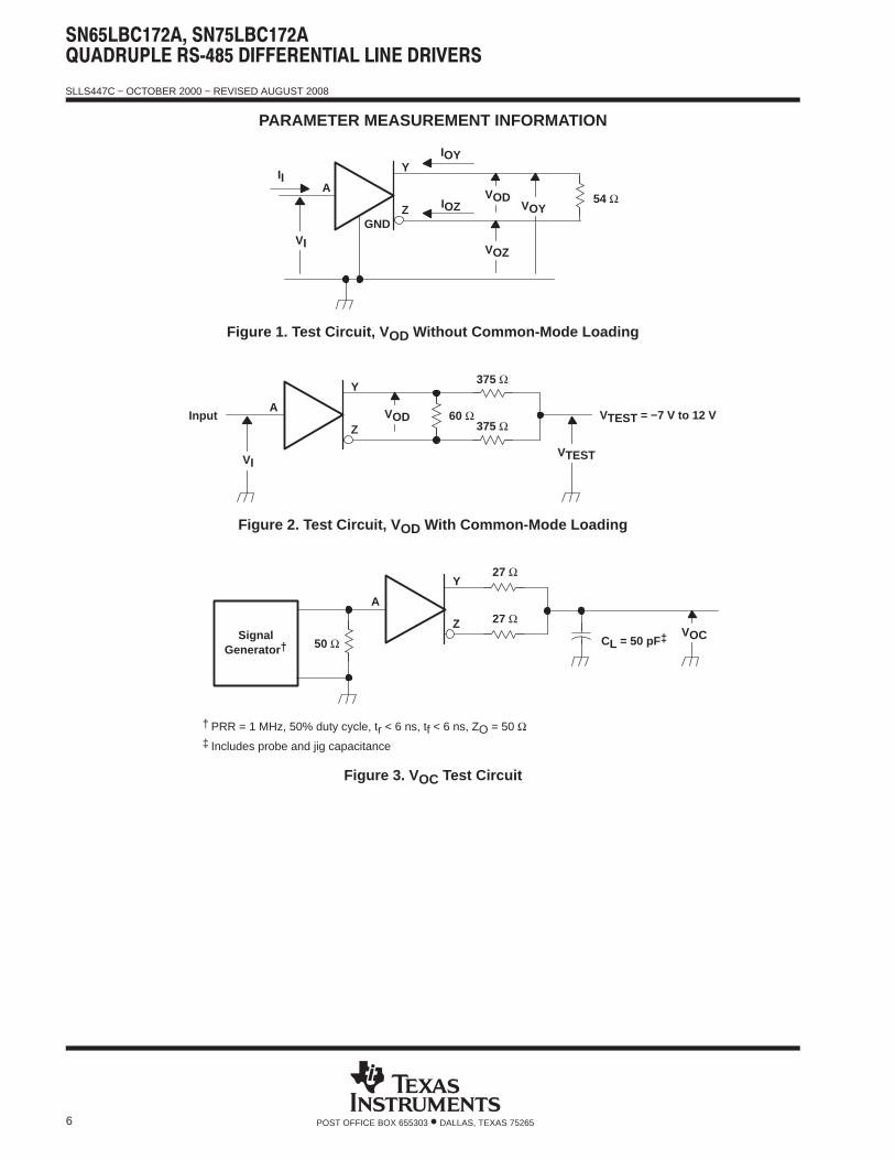
PARAMETER MEASUREMENT INFORMATION
GNDVI
AIOZ
IOYY
ZVOD
VOY
II
VOZ
54 Ω
Figure 1. Test Circuit, V OD Without Common-Mode Loading
375 Ω
VTEST = −7 V to 12 V
Y
ZVODInput 60 Ω
375 Ω
VI
A
VTEST
Figure 2. Test Circuit, V OD With Common-Mode Loading
Y
ZVOC
27 Ω
A
50 ΩSignal
Generator † CL = 50 pF‡
27 Ω
† PRR = 1 MHz, 50% duty cycle, tr < 6 ns, tf < 6 ns, ZO = 50 Ω‡ Includes probe and jig capacitance
Figure 3. V OC Test Circuit
SLLS447C − OCTOBER 2000 − REVISED AUGUST 2008
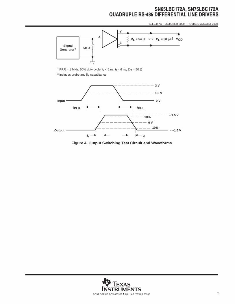
7POST OFFICE BOX 655303 • DALLAS, TEXAS 75265
Y
ZVODRL = 54 Ω
A
50 ΩSignal
Generator †
CL = 50 pF‡
90%
Output
0 V
10%
tf
≈ −1.5 V
≈ 1.5 V
tr
Input 0 V
3 V
tPHL
1.5 V
tPLH
† PRR = 1 MHz, 50% duty cycle, tr < 6 ns, tf < 6 ns, ZO = 50 Ω‡ Includes probe and jig capacitance
Figure 4. Output Switching Test Circuit and Waveforms
SLLS447C − OCTOBER 2000 − REVISED AUGUST 2008
8 POST OFFICE BOX 655303 • DALLAS, TEXAS 75265
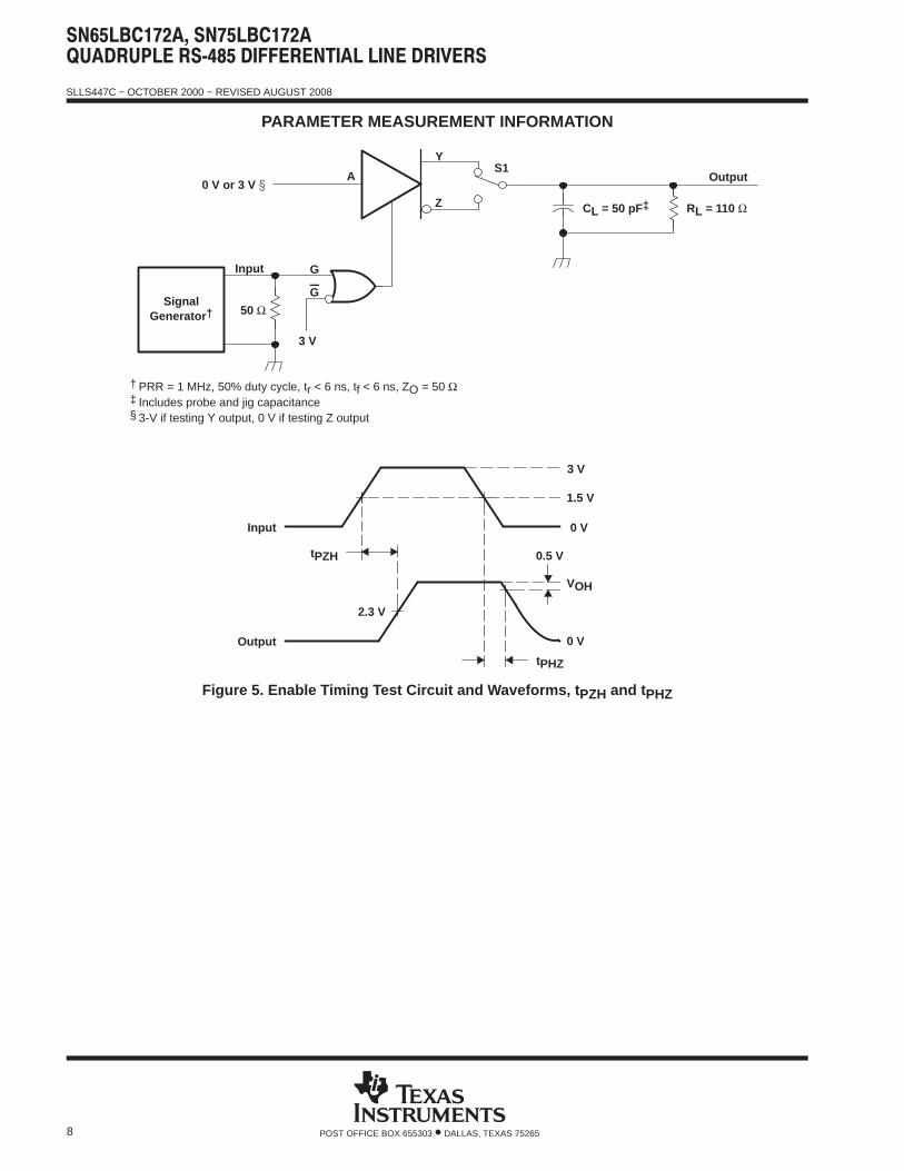
PARAMETER MEASUREMENT INFORMATION
S1A
50 ΩSignal
Generator †
Output
2.3 V
Input 0 V
3 V
1.5 V
tPZH 0.5 V
0 V
VOH
tPHZ
0 V or 3 V
Input
G
G
RL = 110 ΩCL = 50 pF‡
Output
3 V
Y
Z
† PRR = 1 MHz, 50% duty cycle, tr < 6 ns, tf < 6 ns, ZO = 50 Ω‡ Includes probe and jig capacitance§ 3-V if testing Y output, 0 V if testing Z output
Figure 5. Enable Timing Test Circuit and Waveforms, t PZH and t PHZ

SLLS447C − OCTOBER 2000 − REVISED AUGUST 2008
9POST OFFICE BOX 655303 • DALLAS, TEXAS 75265
PARAMETER MEASUREMENT INFORMATION
S1A
50 ΩSignal
Generator †
Output
2.3 V
Input 0 V
3 V
1.5 V
tPZL
0.5 V
5 V
VOL
tPLZ
0 V or 3 V
Input
G
G
RL = 110 Ω
CL = 50 pF‡
Output
3 V
5 V
Y
Z
† PRR = 1 MHz, 50% duty cycle, tr < 6 ns, tf < 6 ns, ZO = 50 Ω‡ Includes probe and jig capacitance§ 3-V if testing Y output, 0 V if testing Z output
Figure 6. Enable Timing Test Circuit and Waveforms, t PZL and t PLZ
SLLS447C − OCTOBER 2000 − REVISED AUGUST 2008
10 POST OFFICE BOX 655303 • DALLAS, TEXAS 75265
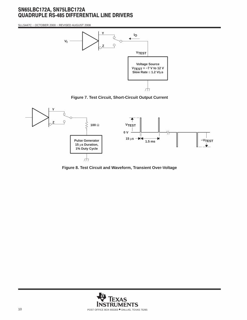
Voltage SourceVTEST = −7 V to 12 VSlew Rate ≤ 1.2 V/µs
VI
VTEST
IOY
Z
Figure 7. Test Circuit, Short-Circuit Output Current
VTEST
Pulse Generator15 µs Duration,1% Duty Cycle
100 Ω
Y
Z
−VTEST15 µs
1.5 ms
0 V
Figure 8. Test Circuit and Waveform, Transient Over-Voltage
SLLS447C − OCTOBER 2000 − REVISED AUGUST 2008
11POST OFFICE BOX 655303 • DALLAS, TEXAS 75265
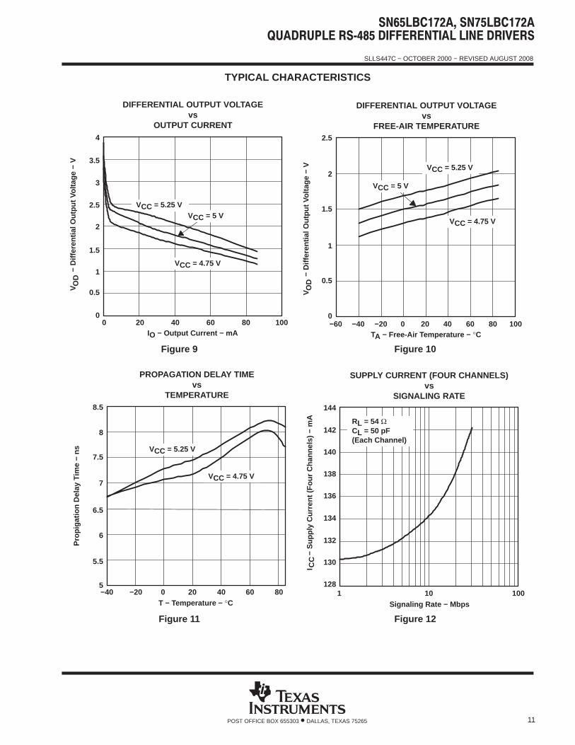
TYPICAL CHARACTERISTICS
Figure 9
0
0.5
1
1.5
2
2.5
3
3.5
4
0 20 40 60 80 100
VCC = 5.25 VVCC = 5 V
VCC = 4.75 V
− D
iffer
entia
l Out
put V
olta
ge −
V
DIFFERENTIAL OUTPUT VOLTAGEvs
OUTPUT CURRENT
IO − Output Current − mA
VO
D
Figure 10
0
0.5
1
1.5
2
2.5
−60 −40 −20 0 20 40 60 80 100
VCC = 5.25 V
VCC = 5 V
VCC = 4.75 V
− D
iffer
entia
l Out
put V
olta
ge −
V
DIFFERENTIAL OUTPUT VOLTAGEvs
FREE-AIR TEMPERATURE
VO
D
TA − Free-Air Temperature − °C
Figure 11
5
5.5
6
6.5
7
7.5
8
8.5
−40 −20 0 20 40 60 80
VCC = 5.25 V
VCC = 4.75 V
Pro
piga
tion
Del
ay T
ime
− ns
PROPAGATION DELAY TIMEvs
TEMPERATURE
T − Temperature − °C
Figure 12
128
130
132
134
136
138
140
142
144
1 10 100
− S
uppl
y C
urre
nt (
Fou
r C
hann
els)
− m
A
Signaling Rate − Mbps
SUPPLY CURRENT (FOUR CHANNELS)vs
SIGNALING RATE
I CC
RL = 54 ΩCL = 50 pF(Each Channel)
SLLS447C − OCTOBER 2000 − REVISED AUGUST 2008
12 POST OFFICE BOX 655303 • DALLAS, TEXAS 75265
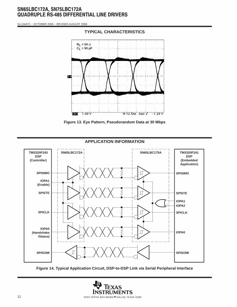
TYPICAL CHARACTERISTICS
RL = 54 ΩCL = 50 pF
Figure 13. Eye Pattern, Pseudorandom Data at 30 Mbps
APPLICATION INFORMATION
TMS320F243DSP
(Controller)
SPISIMO
SN65LBC172A SN65LBC175A TMS320F241DSP
(EmbeddedApplication)
SPISIMO
IOPA1
SPISTE SPISTE
IOPA0(Handshake
/Status)
SPICLK
IOPA0
IOPA1(Enable)
SPICLK
SPISOMI SPISOMI
IOPA2
Figure 14. Typical Application Circuit, DSP-to-DSP Link via Serial Peripheral Interface
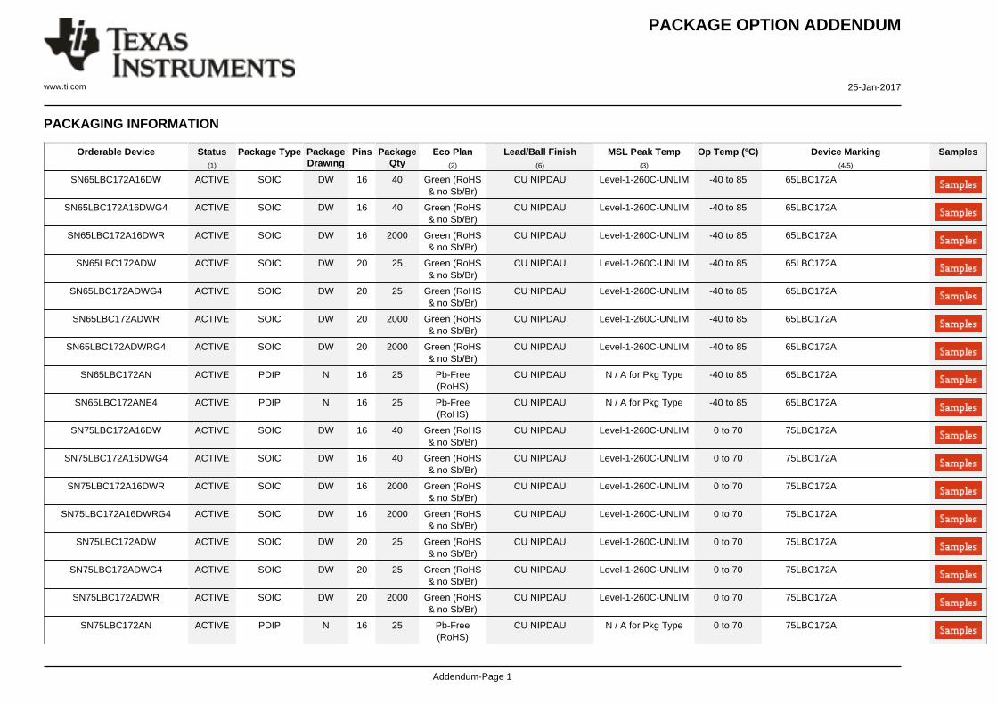
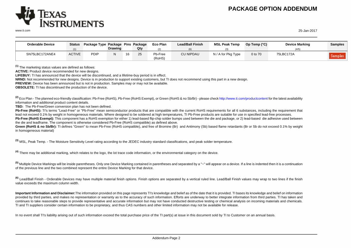
PACKAGE OPTION ADDENDUM
www.ti.com 25-Jan-2017
Addendum-Page 1
PACKAGING INFORMATION
Orderable Device Status(1)
Package Type PackageDrawing
Pins PackageQty
Eco Plan(2)
Lead/Ball Finish(6)
MSL Peak Temp(3)
Op Temp (°C) Device Marking(4/5)
Samples
SN65LBC172A16DW ACTIVE SOIC DW 16 40 Green (RoHS& no Sb/Br)
CU NIPDAU Level-1-260C-UNLIM -40 to 85 65LBC172A
SN65LBC172A16DWG4 ACTIVE SOIC DW 16 40 Green (RoHS& no Sb/Br)
CU NIPDAU Level-1-260C-UNLIM -40 to 85 65LBC172A
SN65LBC172A16DWR ACTIVE SOIC DW 16 2000 Green (RoHS& no Sb/Br)
CU NIPDAU Level-1-260C-UNLIM -40 to 85 65LBC172A
SN65LBC172ADW ACTIVE SOIC DW 20 25 Green (RoHS& no Sb/Br)
CU NIPDAU Level-1-260C-UNLIM -40 to 85 65LBC172A
SN65LBC172ADWG4 ACTIVE SOIC DW 20 25 Green (RoHS& no Sb/Br)
CU NIPDAU Level-1-260C-UNLIM -40 to 85 65LBC172A
SN65LBC172ADWR ACTIVE SOIC DW 20 2000 Green (RoHS& no Sb/Br)
CU NIPDAU Level-1-260C-UNLIM -40 to 85 65LBC172A
SN65LBC172ADWRG4 ACTIVE SOIC DW 20 2000 Green (RoHS& no Sb/Br)
CU NIPDAU Level-1-260C-UNLIM -40 to 85 65LBC172A
SN65LBC172AN ACTIVE PDIP N 16 25 Pb-Free(RoHS)
CU NIPDAU N / A for Pkg Type -40 to 85 65LBC172A
SN65LBC172ANE4 ACTIVE PDIP N 16 25 Pb-Free(RoHS)
CU NIPDAU N / A for Pkg Type -40 to 85 65LBC172A
SN75LBC172A16DW ACTIVE SOIC DW 16 40 Green (RoHS& no Sb/Br)
CU NIPDAU Level-1-260C-UNLIM 0 to 70 75LBC172A
SN75LBC172A16DWG4 ACTIVE SOIC DW 16 40 Green (RoHS& no Sb/Br)
CU NIPDAU Level-1-260C-UNLIM 0 to 70 75LBC172A
SN75LBC172A16DWR ACTIVE SOIC DW 16 2000 Green (RoHS& no Sb/Br)
CU NIPDAU Level-1-260C-UNLIM 0 to 70 75LBC172A
SN75LBC172A16DWRG4 ACTIVE SOIC DW 16 2000 Green (RoHS& no Sb/Br)
CU NIPDAU Level-1-260C-UNLIM 0 to 70 75LBC172A
SN75LBC172ADW ACTIVE SOIC DW 20 25 Green (RoHS& no Sb/Br)
CU NIPDAU Level-1-260C-UNLIM 0 to 70 75LBC172A
SN75LBC172ADWG4 ACTIVE SOIC DW 20 25 Green (RoHS& no Sb/Br)
CU NIPDAU Level-1-260C-UNLIM 0 to 70 75LBC172A
SN75LBC172ADWR ACTIVE SOIC DW 20 2000 Green (RoHS& no Sb/Br)
CU NIPDAU Level-1-260C-UNLIM 0 to 70 75LBC172A
SN75LBC172AN ACTIVE PDIP N 16 25 Pb-Free(RoHS)
CU NIPDAU N / A for Pkg Type 0 to 70 75LBC172A
PACKAGE OPTION ADDENDUM
www.ti.com 25-Jan-2017
Addendum-Page 2
Orderable Device Status(1)
Package Type PackageDrawing
Pins PackageQty
Eco Plan(2)
Lead/Ball Finish(6)
MSL Peak Temp(3)
Op Temp (°C) Device Marking(4/5)
Samples
SN75LBC172ANE4 ACTIVE PDIP N 16 25 Pb-Free(RoHS)
CU NIPDAU N / A for Pkg Type 0 to 70 75LBC172A
(1) The marketing status values are defined as follows:ACTIVE: Product device recommended for new designs.LIFEBUY: TI has announced that the device will be discontinued, and a lifetime-buy period is in effect.NRND: Not recommended for new designs. Device is in production to support existing customers, but TI does not recommend using this part in a new design.PREVIEW: Device has been announced but is not in production. Samples may or may not be available.OBSOLETE: TI has discontinued the production of the device.
(2) Eco Plan - The planned eco-friendly classification: Pb-Free (RoHS), Pb-Free (RoHS Exempt), or Green (RoHS & no Sb/Br) - please check http://www.ti.com/productcontent for the latest availabilityinformation and additional product content details.TBD: The Pb-Free/Green conversion plan has not been defined.Pb-Free (RoHS): TI's terms "Lead-Free" or "Pb-Free" mean semiconductor products that are compatible with the current RoHS requirements for all 6 substances, including the requirement thatlead not exceed 0.1% by weight in homogeneous materials. Where designed to be soldered at high temperatures, TI Pb-Free products are suitable for use in specified lead-free processes.Pb-Free (RoHS Exempt): This component has a RoHS exemption for either 1) lead-based flip-chip solder bumps used between the die and package, or 2) lead-based die adhesive used betweenthe die and leadframe. The component is otherwise considered Pb-Free (RoHS compatible) as defined above.Green (RoHS & no Sb/Br): TI defines "Green" to mean Pb-Free (RoHS compatible), and free of Bromine (Br) and Antimony (Sb) based flame retardants (Br or Sb do not exceed 0.1% by weightin homogeneous material)
(3) MSL, Peak Temp. - The Moisture Sensitivity Level rating according to the JEDEC industry standard classifications, and peak solder temperature.
(4) There may be additional marking, which relates to the logo, the lot trace code information, or the environmental category on the device.
(5) Multiple Device Markings will be inside parentheses. Only one Device Marking contained in parentheses and separated by a "~" will appear on a device. If a line is indented then it is a continuationof the previous line and the two combined represent the entire Device Marking for that device.
(6) Lead/Ball Finish - Orderable Devices may have multiple material finish options. Finish options are separated by a vertical ruled line. Lead/Ball Finish values may wrap to two lines if the finishvalue exceeds the maximum column width.
Important Information and Disclaimer:The information provided on this page represents TI's knowledge and belief as of the date that it is provided. TI bases its knowledge and belief on informationprovided by third parties, and makes no representation or warranty as to the accuracy of such information. Efforts are underway to better integrate information from third parties. TI has taken andcontinues to take reasonable steps to provide representative and accurate information but may not have conducted destructive testing or chemical analysis on incoming materials and chemicals.TI and TI suppliers consider certain information to be proprietary, and thus CAS numbers and other limited information may not be available for release.
In no event shall TI's liability arising out of such information exceed the total purchase price of the TI part(s) at issue in this document sold by TI to Customer on an annual basis.
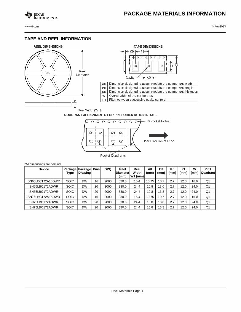
TAPE AND REEL INFORMATION
*All dimensions are nominal
Device PackageType
PackageDrawing
Pins SPQ ReelDiameter
(mm)
ReelWidth
W1 (mm)
A0(mm)
B0(mm)
K0(mm)
P1(mm)
W(mm)
Pin1Quadrant
SN65LBC172A16DWR SOIC DW 16 2000 330.0 16.4 10.75 10.7 2.7 12.0 16.0 Q1
SN65LBC172ADWR SOIC DW 20 2000 330.0 24.4 10.8 13.0 2.7 12.0 24.0 Q1
SN65LBC172ADWR SOIC DW 20 2000 330.0 24.4 10.8 13.3 2.7 12.0 24.0 Q1
SN75LBC172A16DWR SOIC DW 16 2000 330.0 16.4 10.75 10.7 2.7 12.0 16.0 Q1
SN75LBC172ADWR SOIC DW 20 2000 330.0 24.4 10.8 13.0 2.7 12.0 24.0 Q1
SN75LBC172ADWR SOIC DW 20 2000 330.0 24.4 10.8 13.3 2.7 12.0 24.0 Q1
PACKAGE MATERIALS INFORMATION
www.ti.com 4-Jan-2013
Pack Materials-Page 1
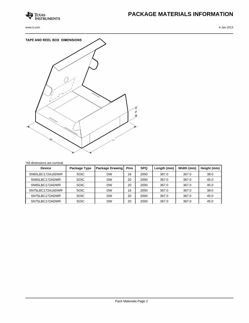
*All dimensions are nominal
Device Package Type Package Drawing Pins SPQ Length (mm) Width (mm) Height (mm)
SN65LBC172A16DWR SOIC DW 16 2000 367.0 367.0 38.0
SN65LBC172ADWR SOIC DW 20 2000 367.0 367.0 45.0
SN65LBC172ADWR SOIC DW 20 2000 367.0 367.0 45.0
SN75LBC172A16DWR SOIC DW 16 2000 367.0 367.0 38.0
SN75LBC172ADWR SOIC DW 20 2000 367.0 367.0 45.0
SN75LBC172ADWR SOIC DW 20 2000 367.0 367.0 45.0
PACKAGE MATERIALS INFORMATION
www.ti.com 4-Jan-2013
Pack Materials-Page 2
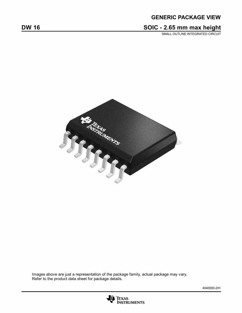
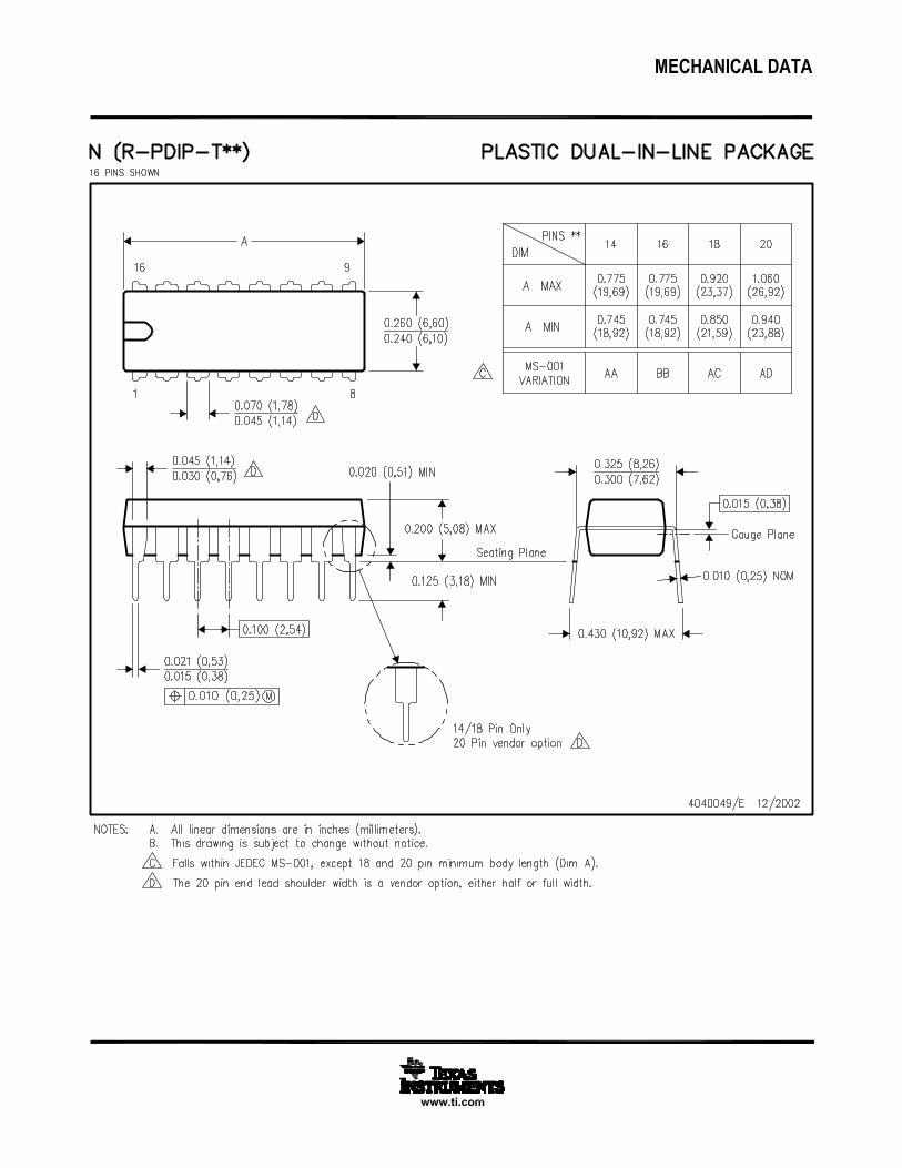
GENERIC PACKAGE VIEW
Images above are just a representation of the package family, actual package may vary.Refer to the product data sheet for package details.
DW 16 SOIC - 2.65 mm max heightSMALL OUTLINE INTEGRATED CIRCUIT
4040000-2/H
www.ti.com
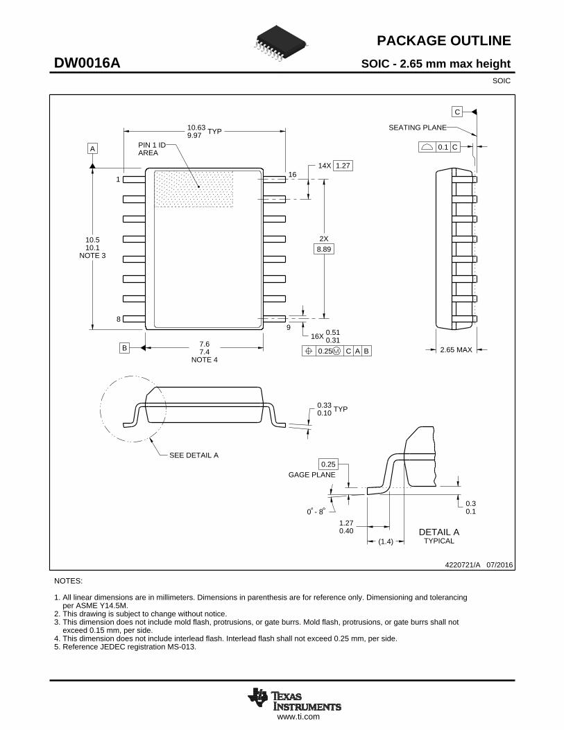
PACKAGE OUTLINE
C
TYP10.639.97
2.65 MAX
14X 1.27
16X 0.510.31
2X8.89
TYP0.330.10
0 - 80.30.1
(1.4)
0.25GAGE PLANE
1.270.40
A
NOTE 3
10.510.1
BNOTE 4
7.67.4
4220721/A 07/2016
SOIC - 2.65 mm max heightDW0016ASOIC
NOTES: 1. All linear dimensions are in millimeters. Dimensions in parenthesis are for reference only. Dimensioning and tolerancing per ASME Y14.5M. 2. This drawing is subject to change without notice. 3. This dimension does not include mold flash, protrusions, or gate burrs. Mold flash, protrusions, or gate burrs shall not exceed 0.15 mm, per side. 4. This dimension does not include interlead flash. Interlead flash shall not exceed 0.25 mm, per side.5. Reference JEDEC registration MS-013.
1 16
0.25 C A B
98
PIN 1 IDAREA
SEATING PLANE
0.1 C
SEE DETAIL A
DETAIL ATYPICAL
SCALE 1.500
www.ti.com
EXAMPLE BOARD LAYOUT
0.07 MAXALL AROUND
0.07 MINALL AROUND
(9.3)
14X (1.27)
R0.05 TYP
16X (2)
16X (0.6)
4220721/A 07/2016
SOIC - 2.65 mm max heightDW0016ASOIC
NOTES: (continued) 6. Publication IPC-7351 may have alternate designs. 7. Solder mask tolerances between and around signal pads can vary based on board fabrication site.
METAL SOLDER MASKOPENING
NON SOLDER MASKDEFINED
SOLDER MASK DETAILS
OPENINGSOLDER MASK METAL
SOLDER MASKDEFINED
LAND PATTERN EXAMPLESCALE:7X
SYMM
1
8 9
16
SEEDETAILS
SYMM
www.ti.com
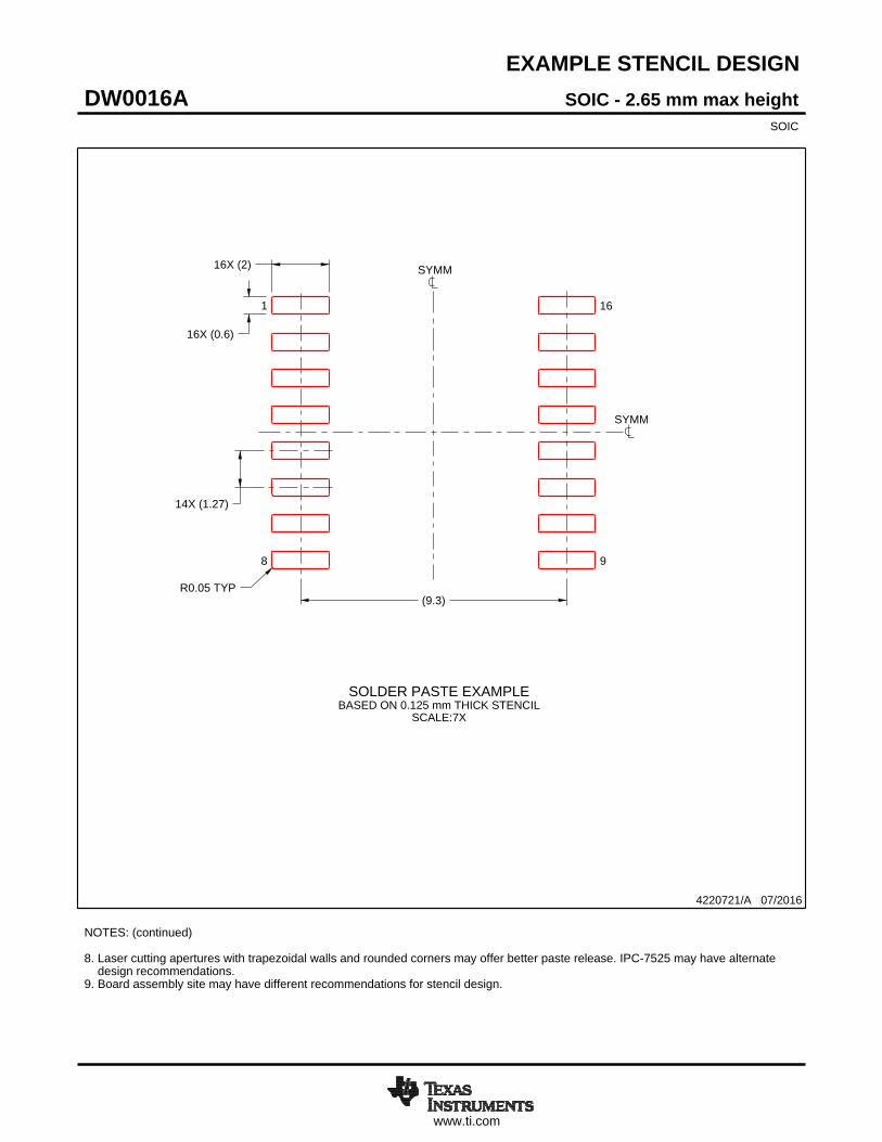
EXAMPLE STENCIL DESIGN
R0.05 TYP
16X (2)
16X (0.6)
14X (1.27)
(9.3)
4220721/A 07/2016
SOIC - 2.65 mm max heightDW0016ASOIC
NOTES: (continued) 8. Laser cutting apertures with trapezoidal walls and rounded corners may offer better paste release. IPC-7525 may have alternate design recommendations. 9. Board assembly site may have different recommendations for stencil design.
SOLDER PASTE EXAMPLEBASED ON 0.125 mm THICK STENCIL
SCALE:7X
SYMM
SYMM
1
8 9
16
www.ti.com
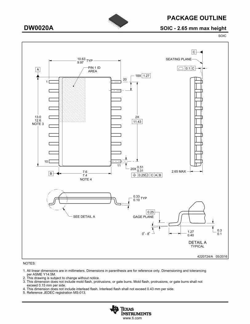
PACKAGE OUTLINE
C
TYP10.639.97
2.65 MAX
18X 1.27
20X 0.510.31
2X11.43
TYP0.330.10
0 - 80.30.1
0.25GAGE PLANE
1.270.40
A
NOTE 3
13.012.6
B 7.67.4
4220724/A 05/2016
SOIC - 2.65 mm max heightDW0020ASOIC
NOTES: 1. All linear dimensions are in millimeters. Dimensions in parenthesis are for reference only. Dimensioning and tolerancing per ASME Y14.5M. 2. This drawing is subject to change without notice. 3. This dimension does not include mold flash, protrusions, or gate burrs. Mold flash, protrusions, or gate burrs shall not exceed 0.15 mm per side. 4. This dimension does not include interlead flash. Interlead flash shall not exceed 0.43 mm per side.5. Reference JEDEC registration MS-013.
120
0.25 C A B
1110
PIN 1 IDAREA
NOTE 4
SEATING PLANE
0.1 C
SEE DETAIL A
DETAIL ATYPICAL
SCALE 1.200
www.ti.com
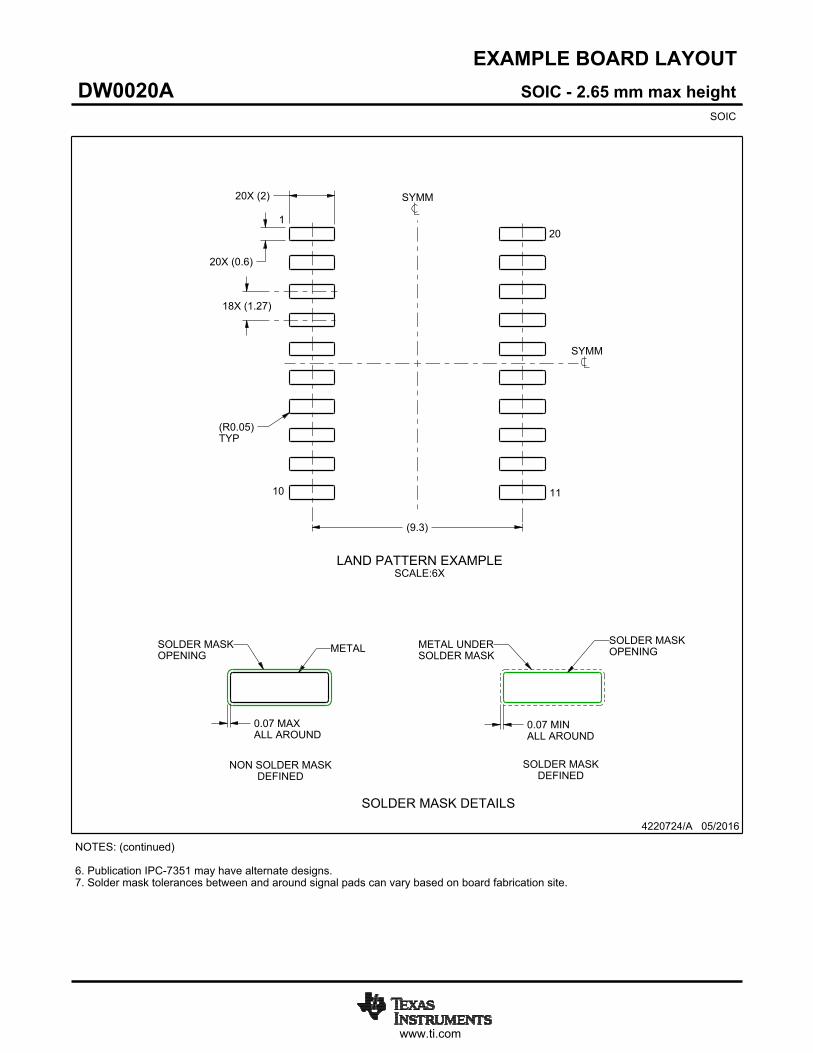
EXAMPLE BOARD LAYOUT
(9.3)
0.07 MAXALL AROUND
0.07 MINALL AROUND
20X (2)
20X (0.6)
18X (1.27)
(R )TYP
0.05
4220724/A 05/2016
SOIC - 2.65 mm max heightDW0020ASOIC
SYMM
SYMM
LAND PATTERN EXAMPLESCALE:6X
1
10 11
20
NOTES: (continued) 6. Publication IPC-7351 may have alternate designs. 7. Solder mask tolerances between and around signal pads can vary based on board fabrication site.
METALSOLDER MASKOPENING
NON SOLDER MASKDEFINED
SOLDER MASK DETAILS
SOLDER MASKOPENING
METAL UNDERSOLDER MASK
SOLDER MASKDEFINED
www.ti.com
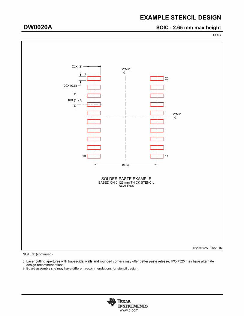
EXAMPLE STENCIL DESIGN
(9.3)
18X (1.27)
20X (0.6)
20X (2)
4220724/A 05/2016
SOIC - 2.65 mm max heightDW0020ASOIC
NOTES: (continued) 8. Laser cutting apertures with trapezoidal walls and rounded corners may offer better paste release. IPC-7525 may have alternate design recommendations. 9. Board assembly site may have different recommendations for stencil design.
SYMM
SYMM
1
10 11
20
SOLDER PASTE EXAMPLEBASED ON 0.125 mm THICK STENCIL
SCALE:6X
IMPORTANT NOTICE
Texas Instruments Incorporated (TI) reserves the right to make corrections, enhancements, improvements and other changes to itssemiconductor products and services per JESD46, latest issue, and to discontinue any product or service per JESD48, latest issue. Buyersshould obtain the latest relevant information before placing orders and should verify that such information is current and complete.TI’s published terms of sale for semiconductor products (http://www.ti.com/sc/docs/stdterms.htm) apply to the sale of packaged integratedcircuit products that TI has qualified and released to market. Additional terms may apply to the use or sale of other types of TI products andservices.Reproduction of significant portions of TI information in TI data sheets is permissible only if reproduction is without alteration and isaccompanied by all associated warranties, conditions, limitations, and notices. TI is not responsible or liable for such reproduceddocumentation. Information of third parties may be subject to additional restrictions. Resale of TI products or services with statementsdifferent from or beyond the parameters stated by TI for that product or service voids all express and any implied warranties for theassociated TI product or service and is an unfair and deceptive business practice. TI is not responsible or liable for any such statements.Buyers and others who are developing systems that incorporate TI products (collectively, “Designers”) understand and agree that Designersremain responsible for using their independent analysis, evaluation and judgment in designing their applications and that Designers havefull and exclusive responsibility to assure the safety of Designers' applications and compliance of their applications (and of all TI productsused in or for Designers’ applications) with all applicable regulations, laws and other applicable requirements. Designer represents that, withrespect to their applications, Designer has all the necessary expertise to create and implement safeguards that (1) anticipate dangerousconsequences of failures, (2) monitor failures and their consequences, and (3) lessen the likelihood of failures that might cause harm andtake appropriate actions. Designer agrees that prior to using or distributing any applications that include TI products, Designer willthoroughly test such applications and the functionality of such TI products as used in such applications.TI’s provision of technical, application or other design advice, quality characterization, reliability data or other services or information,including, but not limited to, reference designs and materials relating to evaluation modules, (collectively, “TI Resources”) are intended toassist designers who are developing applications that incorporate TI products; by downloading, accessing or using TI Resources in anyway, Designer (individually or, if Designer is acting on behalf of a company, Designer’s company) agrees to use any particular TI Resourcesolely for this purpose and subject to the terms of this Notice.TI’s provision of TI Resources does not expand or otherwise alter TI’s applicable published warranties or warranty disclaimers for TIproducts, and no additional obligations or liabilities arise from TI providing such TI Resources. TI reserves the right to make corrections,enhancements, improvements and other changes to its TI Resources. TI has not conducted any testing other than that specificallydescribed in the published documentation for a particular TI Resource.Designer is authorized to use, copy and modify any individual TI Resource only in connection with the development of applications thatinclude the TI product(s) identified in such TI Resource. NO OTHER LICENSE, EXPRESS OR IMPLIED, BY ESTOPPEL OR OTHERWISETO ANY OTHER TI INTELLECTUAL PROPERTY RIGHT, AND NO LICENSE TO ANY TECHNOLOGY OR INTELLECTUAL PROPERTYRIGHT OF TI OR ANY THIRD PARTY IS GRANTED HEREIN, including but not limited to any patent right, copyright, mask work right, orother intellectual property right relating to any combination, machine, or process in which TI products or services are used. Informationregarding or referencing third-party products or services does not constitute a license to use such products or services, or a warranty orendorsement thereof. Use of TI Resources may require a license from a third party under the patents or other intellectual property of thethird party, or a license from TI under the patents or other intellectual property of TI.TI RESOURCES ARE PROVIDED “AS IS” AND WITH ALL FAULTS. TI DISCLAIMS ALL OTHER WARRANTIES ORREPRESENTATIONS, EXPRESS OR IMPLIED, REGARDING RESOURCES OR USE THEREOF, INCLUDING BUT NOT LIMITED TOACCURACY OR COMPLETENESS, TITLE, ANY EPIDEMIC FAILURE WARRANTY AND ANY IMPLIED WARRANTIES OFMERCHANTABILITY, FITNESS FOR A PARTICULAR PURPOSE, AND NON-INFRINGEMENT OF ANY THIRD PARTY INTELLECTUALPROPERTY RIGHTS. TI SHALL NOT BE LIABLE FOR AND SHALL NOT DEFEND OR INDEMNIFY DESIGNER AGAINST ANY CLAIM,INCLUDING BUT NOT LIMITED TO ANY INFRINGEMENT CLAIM THAT RELATES TO OR IS BASED ON ANY COMBINATION OFPRODUCTS EVEN IF DESCRIBED IN TI RESOURCES OR OTHERWISE. IN NO EVENT SHALL TI BE LIABLE FOR ANY ACTUAL,DIRECT, SPECIAL, COLLATERAL, INDIRECT, PUNITIVE, INCIDENTAL, CONSEQUENTIAL OR EXEMPLARY DAMAGES INCONNECTION WITH OR ARISING OUT OF TI RESOURCES OR USE THEREOF, AND REGARDLESS OF WHETHER TI HAS BEENADVISED OF THE POSSIBILITY OF SUCH DAMAGES.Unless TI has explicitly designated an individual product as meeting the requirements of a particular industry standard (e.g., ISO/TS 16949and ISO 26262), TI is not responsible for any failure to meet such industry standard requirements.Where TI specifically promotes products as facilitating functional safety or as compliant with industry functional safety standards, suchproducts are intended to help enable customers to design and create their own applications that meet applicable functional safety standardsand requirements. Using products in an application does not by itself establish any safety features in the application. Designers mustensure compliance with safety-related requirements and standards applicable to their applications. Designer may not use any TI products inlife-critical medical equipment unless authorized officers of the parties have executed a special contract specifically governing such use.Life-critical medical equipment is medical equipment where failure of such equipment would cause serious bodily injury or death (e.g., lifesupport, pacemakers, defibrillators, heart pumps, neurostimulators, and implantables). Such equipment includes, without limitation, allmedical devices identified by the U.S. Food and Drug Administration as Class III devices and equivalent classifications outside the U.S.TI may expressly designate certain products as completing a particular qualification (e.g., Q100, Military Grade, or Enhanced Product).Designers agree that it has the necessary expertise to select the product with the appropriate qualification designation for their applicationsand that proper product selection is at Designers’ own risk. Designers are solely responsible for compliance with all legal and regulatoryrequirements in connection with such selection.Designer will fully indemnify TI and its representatives against any damages, costs, losses, and/or liabilities arising out of Designer’s non-compliance with the terms and provisions of this Notice.
Mailing Address: Texas Instruments, Post Office Box 655303, Dallas, Texas 75265Copyright © 2018, Texas Instruments Incorporated