$ 75,'(17 6&+2/$5 352-(&7 5(3257 · and personal mentors that i’ve had at the naval...
TRANSCRIPT


Form Approved OMB No. 0704-0188
(DD-MM-YYYY)
(From - To)
(include area
code)


1
1 Abstract
Abstract
Detection and transmission of weak radio-frequency (RF) signals poses a significant chal-lenge for modern electronic systems, in which lossy copper wires and thermal noise can corruptsensitive information. Conversion, or “transduction” of these signals into the optical domain,however, enables enhanced detection sensitivity as well as long distance, low-loss transmissionin optical fibers. Mechanically mediated transduction architectures, which rely upon the cou-pling of electronic and optical signals to a common mechanical oscillator, have sparked recentresearch interest for this application due to their ability to efficiently couple signals of drasti-cally different frequencies. Recent advances in photonic integrated circuits (PICs), which enablethe manufacture of complex optical circuits, have demonstrated the potential to integrate me-chanical resonators into optical designs, and therefore serve as an ideal platform for transducerdevelopment.
Here, extending upon previous work on sensitive optomechanical interactions, we explore anovel, fully integrated technique for RF-to-optical transduction. In the proposed system, an RFsignal displaces a coupled mechanical resonator placed within the evanescent field of an opticalwaveguide. This resulting displacement subsequently induces an optical phase shift due to theresonator’s proximity to the underlying optical waveguide. Placing this “phase shifter” within aninterferometer enables sensitive optical phase detection, thus completing the conversion from anRF to an optical signal. To quantify the expected device performance, a theoretical model wasdeveloped and evaluated based upon the results of computational finite element simulations. Acomplete fabrication cycle was then conducted at the Naval Research Laboratory’s NanoscienceInstitute, which yielded devices for experimental verification of these conclusions and enableda proof-of-concept implementation of the proposed architecture. This research thus provides acomplete theoretical, computational, and experimental characterization of a novel scheme forRF-to-optical transduction which may have future applications for enhanced sensing and forfundamental research into coherent quantum state transfer.
Keywords: integrated photonics, micro-electro-mechanical systems, RF-to-optical trans-duction, mechanically mediated transduction, optomechanics, optical modulation

2
2 Acknowledgments
There are unfortunately far too many people that I have to thank than can fit on this page...
I’ll start with my advisors on this project at the Naval Academy, who have continuously and gra-ciously offered me their knowledge, support, and expertise over the past few years. After intentlysearching for research projects to work on at the Academy, Professor Mungan was the first to bringme into his lab and to get me started working on an undergraduate research project. Around thesame time, Professor Mechtel was my electromagnetics professor, and encouraged me to pursue myinterests outside of the classroom. Prof. Jenkins, my academic and research adviser, has alwaysbeen an excellent sounding board for ideas, and somehow still puts up with me randomly droppingby his office. Professor Frigo, who got the ball rolling on this project by putting me in touch withDr. Stievater’s group at the Naval Research Laboratory, never lets me walk away from our discus-sions without having learned something new and having thought of a new question (or wonderingwhere his pop culture references come from).
It goes without saying that I couldn’t be more thankful for the rest of my classroom professorsand personal mentors that I’ve had at the Naval Academy, all of whom have developed me intothe person who I am today. Capt Cory Kampf, Professor Firebaugh, Professor Blanco, ProfessorMcCarthy, Professor Brereton, and LCDR Wood are a few of those who have been especially in-fluential. Reaching back to my time at the North Carolina School of Science and Math, I thinkit’s safe to say that I’d never be where I am today without having met Dr. John Kolena, who hasbeen the ultimate teacher, mentor, and friend. Don’t worry John, I’m still working on my culturalliteracy...
At the Naval Research Laboratory, I can’t thank Dr. Marcel Pruessner enough for letting me cometo work with him and the rest of Code 5654 – without their support, this work surely would nothave been possible. And of course, how could I not thank Dr. Dmitry Kozak for his constant jokesand for welcoming me into the underground NRL cleanroom arm wrestling bracket...
As for funding, I was fortunate enough to be supported by the USNA Trident Scholar program aswell as the Stamps Leadership Scholarship. Their financial support was invaluable, and providedme with a wonderful experience that I’ll always remember with great fondness.
Finally, I can never thank my family – my mother and father, as well as my two awesome brothersPatrick and Benjamin – enough for their support and never-ending sense of humor. You guys arethe best.

3
Contents
1 Abstract 1
2 Acknowledgments 2
3 Introduction 5
4 Transduction Architecture 74.1 Electromechanical Coupling . . . . . . . . . . . . . . . . . . . . . . . . . . . . . . . . 84.2 Optomechanical Coupling . . . . . . . . . . . . . . . . . . . . . . . . . . . . . . . . . 84.3 Phase Shift Readout . . . . . . . . . . . . . . . . . . . . . . . . . . . . . . . . . . . . 114.4 Summary . . . . . . . . . . . . . . . . . . . . . . . . . . . . . . . . . . . . . . . . . . 12
5 Transduction Theory 135.1 Overview and Direction . . . . . . . . . . . . . . . . . . . . . . . . . . . . . . . . . . 14
6 Electromechanical Simulation 156.1 Geometries . . . . . . . . . . . . . . . . . . . . . . . . . . . . . . . . . . . . . . . . . 156.2 Resonant Frequency . . . . . . . . . . . . . . . . . . . . . . . . . . . . . . . . . . . . 166.3 DC Bias Study . . . . . . . . . . . . . . . . . . . . . . . . . . . . . . . . . . . . . . . 18
6.3.1 Capacitive Spring Softening . . . . . . . . . . . . . . . . . . . . . . . . . . . . 196.3.2 Electrostatic Tuning . . . . . . . . . . . . . . . . . . . . . . . . . . . . . . . . 20
6.4 Summary . . . . . . . . . . . . . . . . . . . . . . . . . . . . . . . . . . . . . . . . . . 21
7 Optomechanical Simulation 237.1 2D Perturber Test Results . . . . . . . . . . . . . . . . . . . . . . . . . . . . . . . . . 23
8 Expected Performance 258.1 Summary and Direction . . . . . . . . . . . . . . . . . . . . . . . . . . . . . . . . . . 27
9 Device Fabrication 28
10 Experimental Design and Methodology 33
11 Experimental Results and Analysis 36
12 Discussion and Future Work 43
13 Conclusions 44
Appendix A Transfer Function Derivations 48A.1 Method 1: Bare Transducer . . . . . . . . . . . . . . . . . . . . . . . . . . . . . . . . 48
A.1.1 Equations of Motion . . . . . . . . . . . . . . . . . . . . . . . . . . . . . . . . 48A.1.2 Signal Readout . . . . . . . . . . . . . . . . . . . . . . . . . . . . . . . . . . . 49
A.2 Method II: LC Coupled System . . . . . . . . . . . . . . . . . . . . . . . . . . . . . . 50A.2.1 Equation of Motion – DC Biased . . . . . . . . . . . . . . . . . . . . . . . . . 50A.2.2 Signal Readout . . . . . . . . . . . . . . . . . . . . . . . . . . . . . . . . . . . 52A.2.3 Equation of Motion – AC Biased . . . . . . . . . . . . . . . . . . . . . . . . . 52

4
Appendix B Mach-Zehnder Interferometer Transfer Function Derivation 53
Appendix C Theoretical Analysis of the LC Coupled Transducer 55C.1 Electromechanical LC Coupled System . . . . . . . . . . . . . . . . . . . . . . . . . . 55
C.1.1 Optimum Coupling and Half-Wave Voltage . . . . . . . . . . . . . . . . . . . 56C.1.2 Default Parameters and Predicted Performance . . . . . . . . . . . . . . . . . 56C.1.3 Device Input Impedance . . . . . . . . . . . . . . . . . . . . . . . . . . . . . . 59C.1.4 Gain from LC Resonator . . . . . . . . . . . . . . . . . . . . . . . . . . . . . 59
Appendix D Transfer Function Behavior, Scaling, and Default Parameters 61D.1 Strong Coupling . . . . . . . . . . . . . . . . . . . . . . . . . . . . . . . . . . . . . . 61D.2 Performance Scaling . . . . . . . . . . . . . . . . . . . . . . . . . . . . . . . . . . . . 62
Appendix E Simulated Performance of LC -based System 65E.1 Electromechanical Coupling . . . . . . . . . . . . . . . . . . . . . . . . . . . . . . . . 65E.2 Achieving Optimal Electromechanical Transduction – Varying L . . . . . . . . . . . 67E.3 Achieving Optimal Electromechanical Transduction – Revised Geometry . . . . . . . 67E.4 Summary . . . . . . . . . . . . . . . . . . . . . . . . . . . . . . . . . . . . . . . . . . 68
Appendix F Comparison of Electrostatic Actuation Techniques 69
Appendix G Microbridge Design Optimization 71
Appendix H Optomechanical Coupling Optimization 73H.1 Waveguide Optimization . . . . . . . . . . . . . . . . . . . . . . . . . . . . . . . . . . 73H.2 Perturber Optimization . . . . . . . . . . . . . . . . . . . . . . . . . . . . . . . . . . 74H.3 Thin Film High-Index Cladding . . . . . . . . . . . . . . . . . . . . . . . . . . . . . . 74
Appendix I Experimental Challenges – Stiction Failure 77
Appendix J Experimental Challenges – Electrical Pickup Isolation 79
5
3 Introduction
The transmission and detection of weak radio-frequency (RF) signals – signals with frequenciesbetween 3 kHz and 300 MHz – is of direct importance to naval missions which rely upon precisionsignals intelligence, surveillance, and reconnaissance operations worldwide. However, these pro-cesses also pose a significant challenge for modern electronic systems, in which lossy copper wiresand thermal noise can corrupt or mask sensitive information. Converting, or “transducing,” thesesignals into optical signals, however, enables enhanced detection sensitivity as well as long distance,low-loss transmission in fiber optic systems [1].
Recent research in optomechanics, a growing field of investigation which explores the interactionbetween light and matter, has sparked interest in the study of of mechanically mediated trans-duction schemes, as RF and optical signals with drastically different frequencies can be coupledto a common mechanical resonator [3]. This approach has been experimentally verified in recentresearch [4, 5, 6]; however, the segmented architectures implemented in these studies impedes theirintegration into deployable systems.
The use of photonic integrated circuits (PICs) affords one possible avenue for integration of mechan-ical structures and micro-electro-mechanical systems (MEMS) into pre-existing optical technologies[13]. In general, the field of integrated photonics allows the traditionally segmented optics com-ponents used for optomechanical investigations to be combined into miniaturized circuits that canbe easily fabricated using mature processes developed within the semiconductor transistor industry.
Here, we leverage these capabilities of integrated photonics to explore a novel, fully integratedelectro-opto-mechanical technique for RF-to-optical transduction. Specifically, we extend upon aprevious study [12] which investigated the tunable interaction between an electrostatically-actuatedmechanical resonator and an on-chip optical signal. This technique is extended from a static DCcharacterization to a more general dynamic RF analysis. The proposed approach may have ad-vantages over traditional transduction techniques such as thermo-optic and electro-optic methodswhich rely upon relatively weak effects and thus require significant input power or long interactionlengths to operate efficiently [2].
If fully integrated, an efficient electro-opto-mechanical transducer for RF and optical signals wouldserve as a compact, scalable solution for the sensitive detection of weak electrical signals – a feat ofcrucial importance for a variety of fields challenged with detection of small signals buried below ther-mal noise floors. Although this project involves a fundamental exploration of performance at thedevice level, several system-level applications could be envisioned given the realization of an idealRF-to-optical transducer. For example, large, expensive, cryogenically-cooled pre-amplifiers usedto eliminate thermal Johnson noise in radio astronomy receivers could be replaced by this noise-tolerant transducer, thus dramatically reducing the system’s size and cost [7]. Such a transducermay also enable low-loss transmission of faint electronic signals or quantum coherent upconversionand transmission of sensitive low-frequency quantum states [4]. Seeing the numerous feasible de-fense applications, DARPA has initiated several projects to advance the constituent technologiesinvolved within this project [8, 9].
However, before these future applications can be pursued, the appropriate underlying technologiesmust be fully explored and characterized. This research comprises a complete theoretical, computa-

6
tional, and experimental investigation of a newly proposed method for RF-to-optical transduction,and thus advances this ongoing active field of research.

7
4 Transduction Architecture
Due to their ability to transfer energy and information across different domains, transducers havebecome essential enablers of numerous technologies ranging from everyday smartphones and sensorsto complex naval systems. A typical loudspeaker, for example, converts an input electrical signalinto the mechanical motion of a membrane, which in turn produces an audible pressure wave inair – a physical representation of the original electronic information that can be readily interpretedby the human ear. Functioning in reverse, naval hydrophone arrays facilitate the conversion ofacoustic signals, which propagate efficiently in an underwater environment, to electronic signalsthat are easily transmitted, processed, and stored in above-water computer systems.
The principal advantage demonstrated by these two examples – namely the ability to convert en-ergy in one domain, such as electrical, optical, mechanical, or thermal, to energy contained in amore advantageous signal type – is echoed by RF-to-optical transducers. While RF signals mayexperience notable interference and loss in electronic systems, their placement onto an optical “car-rier” enables isolated, low-loss transmission over hundreds of kilometers in optical fiber. The highercarrier frequencies characteristic of optical signals also provides for a larger data carrying capac-ity, or bandwidth. Of note for sensitive naval operations, both line-of-sight optical links as wellas fiber-contained systems afford enhanced data security over traditional electronic transmissiontechniques, which can be intercepted with an appropriately placed antenna or wire-tap.
Figure 1: In a common loudspeaker, an input electrical signal is passed through a wire coil, thusproducing an electrically-dependent magnetic field. Variations in this induced field displace a mag-netic membrane. A pressure wave is then created through the diaphragm’s interaction with thesurrounding air. Likewise, the proposed electro-opto-mechanical transducer leverages the electro-static force created by applying a bias voltage across a mechanical oscillator – a MEMS microbridgein this case – to yield a parametric displacement. As the microbridge enters more deeply into the“evanescent field” (pale blue to red in figure), it changes the index of refraction of the guided light(“input” to “output”). This, in turn, causes a small change in the optical phase of the output light.
As shown in Figure 1, our proposed transduction technique for this favorable conversion is an op-tical analog to the aforementioned loudspeaker. In both systems, a mechanical resonator is usedto communicate interactions between the input and output signals. For these mechanically me-diated transducers, two key conversions are required: 1) the input signal must first displace themechanical device, and 2) this displacement must then impart some measurable change on a phys-ical parameter of the output signal. In short, both the input and output signals must be mutuallycoupled to a common mechanical structure. For our proposed transduction architecture, we termthese two required processes “electromechanical coupling” and “optomechanical coupling,” respec-

8
tively. Substituting air for light as the medium of information transfer, the mechanically mediatedRF-to-optical conversion process explored here can be qualitatively understood as an “optical loud-speaker” [1].
When integrated, the combination of these two processes yields a complete electro-opto-mechanicaltransducer. A block diagram of our proposed architecture is shown in Figure 2. In the followingsections, each of the conversion processes are described for the proposed architecture.
Figure 2: A schematic depiction of the proposed architecture. Electrical excitations displace amicrobridge oscillator placed within the evanescent field of an optical signal, which in turn creates avariable optical phase shift. When integrated into a Mach-Zehnder interferometer – a sensitive phasedetector – the resulting phase shift modulates the optical intensity at the interferometer’s output.The effectiveness of the RF-to-mechanical and mechanical-to-optical conversion steps are governedby the electromechanical and optomechanical coupling parameters, Gem and Gom respectively.
4.1 Electromechanical Coupling
Here, an electrostatically actuated silicon nitride MEMS (micro-electro-mechanical system) doubly-clamped beam, or “microbridge” [10], is utilized as the system’s mechanical resonator. An image ofa typical bridge is provided in Figure 3. By applying a bias voltage between the suspended bridge’selectrode and a vertically depressed side electrode, the bridge resembles a flexible capacitor whichcan be displaced in a controlled manner via the electrostatic force, �F bridge
electrostatic = −∇Ucapacitor,where Ucapacitor is the potential energy stored in the microbridge capacitor. The coupling efficiencyof this method is theoretically evaluated in Section 5. As a proposed improvement to the elec-tromechanical coupling, the microbridge can be integrated as a portion of the capacitive elementof a LC electrical resonator. This approach, which multiplies the effective voltage applied to themicrobridge, is further explored in Appendix C.
4.2 Optomechanical Coupling
By placing the MEMS microbridge within the evanescent electric field of a propagating optical sig-nal, any electrically-induced bridge displacement yields a slight shift of the optical signal in time,i.e., a “phase shift,” due to a variable optomechanical interaction. The physical mechanism for this

9
Figure 3: Images of suspended microbridges. An overhead view of a 120 μm MEMS silicon nitridesuspended microbridge (red box) with actuation electrodes is shown on the left, while a side profileof a shorter suspended bridge (red), depicting a visible air gap between the bridge and substrate,is on the right. An applied bias between the bridge (red) and side (blue) electrodes can be used todisplace the microbridge.
phase shift is further described here.
To achieve compatibility with existing integrated photonic designs, the mechanical microbridgeis suspended directly above and parallel to an underlying optical waveguide, or “wire” for light.Similar to an optical fiber, this waveguide features a core material with a larger index of refraction“n” than its surrounding layers (air above and silicon dioxide insulator below), and thus utilizes theprinciple of total internal reflection to guide optical signals. Furthermore, the specific waveguideimplemented in this investigation is specifically designed [11] to maximize the fraction of opticalfield lying outside of the waveguide’s core. This exponentially decaying residual electromagneticfield is known as the “evanescent field,” and extends well into the air and oxide layers surroundingthe waveguide core. A two-dimensional cross section of these elements is illustrated in Figure 4.
Figure 4: A illustration of the optomechanical device’s cross section. A suspended microbridge(green) is displaced vertically above an underlying waveguide. The weakly confining silicon nitriderib waveguide (red) is specifically designed to maximize the evanescent field.
When actuated with an electric signal, the bridge penetrates deeper into the evanescent field, thusproducing a variable optical phase shift in the waveguide. More precisely, an optical phase shiftis created by changing the effective index of refraction neff in the waveguide near the displacedbridge. Since the overall phase change, from input to output, is determined by neff, small changesin this parameter result in changes in the optical phase. The effective index, determined by evalu-
10
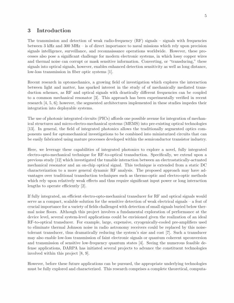
ating the confinement of the optical mode within several materials with different refractive indices,determines the phase propagation speed of light in the region, i.e. vphase = c/neff. Therefore, achange in neff will change the speed of light in the region, thus inducing an optical phase shiftrelative to the signal in the region characterized by the unmodified effective index. This evanescentfield perturbation method, further described in [11], has been utilized in previous devices to createsensitive optical phase shift elements [12].
In the proposed architecture, the effective index is efficiently tuned through this evanescent fieldperturbation method. As depicted by the simulated optical mode profiles shown in Figure 5, dis-placing a silicon nitride (n ≈ 1.8) microbridge further into the evanescent field increases the effectiveindex, since the optical confinement within the bridge, whose refractive index is greater than thatof air (n = 1), increases. As an analogy, consider the waveguide signal to be a fast moving laneof traffic on a highway, and the microbridge to be a lane filled with slow-moving traffic. Whenthe traffic in the fast lane can not see the slow traffic, the cars continue along at their originalspeed. However, when the slow traffic is in sight – an analog of the microbridge being loweredfurther into the optical signal – the fast moving cars naturally slow down as well. Just as theproximity to slow moving traffic influences the average speed of cars on the highway, the heightof the microbridge affects the speed of the optical signal in the waveguide, causing it to shift in time.
Consequently, the coupled microbridge-waveguide optomechanical arrangement forms a sensitive,tunable phase shift element which can be used to effectively modify the properties of an opti-cal signal in response to a mechanical displacement, thus achieving the second required step foran RF-to-optical transducer. When combined with the electrostatic control of the microbridge’sdisplacement through the applied bias voltage, the apparatus constitutes a completely integrateddevice for converting RF input signals into optical phase shifts.
(a) hMEMS = 300 nmneff = 1.53
(b) hMEMS = 200 nmneff = 1.55
(c) hMEMS = 100 nmneff = 1.59
Figure 5: Simulated mode profiles of the weakly-confined rib waveguide described earlier [12] at1550 nm. The magnitude of the horizontal electric field of the fundamental TE mode is representedin color, with blue being the smallest and orange being largest. As hMEMS, the height of the air gapbetween the MEMS perturber and the underlying waveguide, decreases, the effective index increasesexponentially due to greater optical confinement within the silicon nitride perturber (n ≈ 1.8).
11
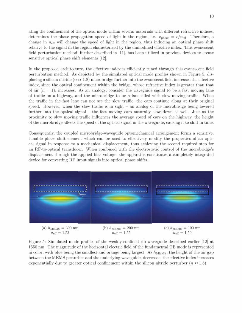
4.3 Phase Shift Readout
The microbridge phase shift element can be incorporated into an integrated photonic interferom-eter, which, serving as a sensitive phase detector, converts small changes in optical phase intoeasily measurable variations in output light intensity. Figure 6 details the key components of theMach-Zehnder interferometers (MZIs) used in this research. In an MZI, input light is separatedinto two separate waveguide “arms.” When these arms are of equal length and no internal phaseshift is added to either arm, the two independent optical signals propagate through to a recombi-nation point at the interferometer output, where they constructively interfere to yield an outputsignal with an equal amplitude as that of the input. Otherwise, if the arms contain a discrete pathlength imbalance, the two recombined signals at the interferometer output have a constant phaseimbalance Δφ which leads to a modified output intensity. For example, if one of the arms is halfan optical wavelength longer than the other, the recombined signals will be π radians out of phase,and will destructively interfere upon recombination to yield zero output intensity.
Figure 6: A Mach-Zehnder interferometer (MZI) can be used to convert small changes in phaseinduced by microbridge displacements into intensity variations in the interferometer’s output signal.As depicted on the left, an MZI splits incident continuous wave laser light into two “arms.” In onearm, the light is delayed due to the presence of the electrically-controlled microbridge perturber.Thus, the intensity of the recombined output light is dependent upon the phase shift impartedwithin the interferometer, and obeys a sinusoidal dependence on this phase imbalance.
The phase imbalance can be tuned by introducing an internal optical phase shift to one of theinterferometer arms. As previously mentioned, the mechanical microbridge coupled to the underly-ing interferometer waveguide serves as this phase shifter for our study. Assuming a phase-matchedcondition in the absence of this perturber, the output optical intensity will vary according to theMZI transfer function
Io =Ii2[1 + cos(Δφ)], (1)
where Io and Ii are the output and input optical intensities, respectively, and Δφ is the bridge-induced phase shift. This relationship between output optical intensity and overall phase imbalance

12
Δφ results in the continuous curve shown on the RHS in Figure 6.
The overall phase shift can be described usefully as composed of two parts: a constant “DC” com-ponent Δφ0 and a time-varying ”ac” component δφ. At any instant of time, the output intensitycan be read off the blue curve’s dependence on the overall phase at that time. Figure 6 shows twocases in which the DC component of the overall phase is changed while the ac component is a givensinusoidal signal. When the DC component is Δφ0 =
3π2 , the operating point for the interferometer
rides up and down the steep part of the blue curve. This creates an optical intensity which isdetected as a voltage variation δVmax. On the other hand, if the DC component were Δφ0 = 0(left trace) the operating point would oscillate along the top of the cosine curve and give a limitedoutput signal, δVmin.
Thus, with a constant DC bias applied to the microbridge, a set phase shift Δφ, which depends onthe change in optomechanical coupling between the bridge and underlying waveguide, is realized.If an RF signal is then applied to the bridge, small mechanical oscillations will yield correspondingfluctuations δφ in the interferometer phase imbalance. These fluctuations, depicted as vertical redsinusoids in Figure 6, yield different output intensity fluctuation amplitudes depending upon theDC bias point. Theoretically, the maximum output fluctuation amplitude is achieved when tunedto a half-power point in which Io(Δφ) = Ii/2. This optimal operation point can be achieved inseveral ways: a fixed length imbalance between the arms; a DC voltage applied to the microbridge;or adjustment of the optical wavelength of light on the interferometer. This last method is the mostpractical, for reasons to be discussed later. From a communications perspective, the MZI enablesthe conversion of phase modulation within the interferometer arm to amplitude modulation of therecombined output signal.
A complete derivation of the theoretical MZI transfer function relating variations in phase, effectiveindex, wavelength, and physical path length imbalance to output intensity is provided in AppendixB. Its characteristics are further discussed in Section 5.
4.4 Summary
In this section, we have introduced the enabling technologies which comprise the proposed RF-to-optical transduction architecture. Namely, the implementation of an electrostatically actuatedmicrobridge realizes the RF-to-optical transduction requirement for an electrically controllabledisplacement of a mechanical resonator. The conversion of displacement to an optical phase shiftis achieved by placing the mechanical microbridge within the evanescent field of a weakly confinedsilicon nitride waveguide. Finally, the RF-to-optical conversion process is completed by integratingthe microbridge phase shifter into an arm of a Mach-Zehnder interferometer, a placement whichenables the optical readout of small phase changes as variations in intensity. Given this background,the overall device theoretical transfer function and performance will now be introduced.
13
5 Transduction Theory
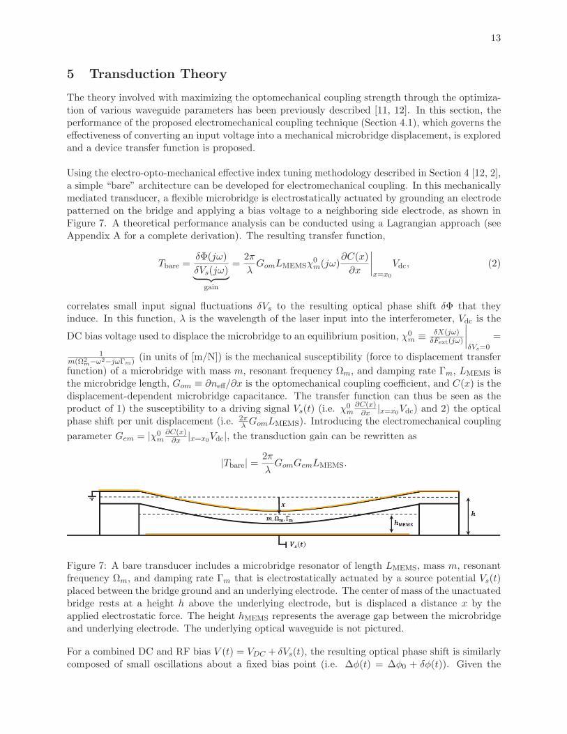
The theory involved with maximizing the optomechanical coupling strength through the optimiza-tion of various waveguide parameters has been previously described [11, 12]. In this section, theperformance of the proposed electromechanical coupling technique (Section 4.1), which governs theeffectiveness of converting an input voltage into a mechanical microbridge displacement, is exploredand a device transfer function is proposed.
Using the electro-opto-mechanical effective index tuning methodology described in Section 4 [12, 2],a simple “bare” architecture can be developed for electromechanical coupling. In this mechanicallymediated transducer, a flexible microbridge is electrostatically actuated by grounding an electrodepatterned on the bridge and applying a bias voltage to a neighboring side electrode, as shown inFigure 7. A theoretical performance analysis can be conducted using a Lagrangian approach (seeAppendix A for a complete derivation). The resulting transfer function,
Tbare =δΦ(jω)
δVs(jω)︸ ︷︷ ︸gain
=2π
λGomLMEMSχ
0m(jω)
∂C(x)
∂x
∣∣∣∣x=x0
Vdc, (2)
correlates small input signal fluctuations δVs to the resulting optical phase shift δΦ that theyinduce. In this function, λ is the wavelength of the laser input into the interferometer, Vdc is the
DC bias voltage used to displace the microbridge to an equilibrium position, χ0m ≡ δX(jω)
δFext(jω)
∣∣∣∣δVs=0
=
1m(Ω2
m−ω2−jωΓm)(in units of [m/N]) is the mechanical susceptibility (force to displacement transfer
function) of a microbridge with mass m, resonant frequency Ωm, and damping rate Γm, LMEMS isthe microbridge length, Gom ≡ ∂neff/∂x is the optomechanical coupling coefficient, and C(x) is thedisplacement-dependent microbridge capacitance. The transfer function can thus be seen as theproduct of 1) the susceptibility to a driving signal Vs(t) (i.e. χ
0m
∂C(x)∂x |x=x0Vdc) and 2) the optical
phase shift per unit displacement (i.e. 2πλ GomLMEMS). Introducing the electromechanical coupling
parameter Gem = |χ0m
∂C(x)∂x |x=x0Vdc|, the transduction gain can be rewritten as
|Tbare| = 2π
λGomGemLMEMS.
Figure 7: A bare transducer includes a microbridge resonator of length LMEMS, mass m, resonantfrequency Ωm, and damping rate Γm that is electrostatically actuated by a source potential Vs(t)placed between the bridge ground and an underlying electrode. The center of mass of the unactuatedbridge rests at a height h above the underlying electrode, but is displaced a distance x by theapplied electrostatic force. The height hMEMS represents the average gap between the microbridgeand underlying electrode. The underlying optical waveguide is not pictured.
For a combined DC and RF bias V (t) = VDC + δVs(t), the resulting optical phase shift is similarlycomposed of small oscillations about a fixed bias point (i.e. Δφ(t) = Δφ0 + δφ(t)). Given the

14
bridge’s placement within the integrated MZI, this phase shift produced by bridge motion modifiesthe interferometer output intensity, which is read out as a voltage Vout on a photodetector. Since thedetected voltage is proportional to the optical intensity, the amplitude of output voltage fluctuationsδVout for a given δφ can be found by differentiating Equation 1 to find
δVout
δφ= −Vi
2sin(Δφ0), (3)
where Δφ0 is the equilibrium interferometer phase offset and Vi is the maximum output voltagewhich corresponds to the input power in a lossless configuration. When biased at a half powerpoint (Δφ0 = π/2, 3π/2, 5π/2, ...) – typically adjusted by varying the input wavelength due to thebuilt in physical path length difference between the two arms of the interferometer – the maximumamplitude of the output voltage fluctuations is found to be
δVout =Vi
2δφ.
This relationship is of fundamental importance to the experimental testing described in Section 10,as it connects the desired transfer function quantity δφ to the measured parameter δVout to enablethe transduction gain |δφ/δVs| to be quantified.
In future design iterations, an integrated LC circuit can be fabricated to improve the electrome-chanical coupling performance. This method, thoroughly explored in Appendices A and C, amplifiesthe voltage across the microbridge capacitor by a factor of QLC , the quality factor of the coupledLC circuit.
5.1 Overview and Direction
The transfer function described here enables a quantitative performance analysis of the entire RF-to-optical transduction system. Mirroring the dependence qualitatively described in Section 4, thetransduction gain – the magnitude of the transfer function |Tbare| – depends on the efficiency oftwo processes: 1) the displacement resulting from an applied electrical bias, and 2) the phase shiftresulting from that electrically-induced displacement. Next, we explore the electromechanical andoptomechanical coupling strengths through a variety of computational multiphysics simulations,and combine these results to predict the overall transduction performance. After establishing thisbaseline numerical understanding of the system, the fabrication of test devices followed by anexperimental verification of the proposed behavior will be described.

15
6 Electromechanical Simulation
To characterize the electromechanical system and quantify the expected electromechanical couplingcoefficient Gem for our device architecture, a computational FEM model was developed in COM-SOL [21] for several different geometries. These models were subsequently used to simulate thedisplacement of an electrostatically actuated microbridge under various conditions.
6.1 Geometries
Three different geometries, shown in Figure 8, were created in COMSOL: one to model a bare mi-crobridge, and two to model the principal electrostatic actuation techniques – direct electrostaticactuation and Kelvin polarization force-based actuation.
(a) Bare (b) Direct Electrostatic (c) Kelvin Polarization Force
Figure 8: Three different geometries designed for FEM simulations in COMSOL. The bare deviceconsists of a silicon nitride (SiNx) MEMS resonator supported by oxide posts which rest on a thinSi3N4 layer with underlying oxide. Gold electrodes are patterned on and beside the bridge fordirect electrostatic actuation, while two side electrodes are patterned beside the bare bridge for thepolarization-induced actuation.
Parameter Value Description
LMEMS 100 μm Length of microbridge
wMEMS 3 μm Width of microbridge
tMEMS 300 nm Microbridge thickness
hMEMS 230 nmThickness of oxide posts supporting
microbridge
tSi3N4 175 nmThickness of stoichiometric silicon nitride
layer above oxide
tSiO2 5 μm Thickness of buried oxide
S0,11/22 variableHorizontal (x/y) intrinsic stress in
PECVD microbridge
Table 1: Geometry dimensions and parameters for bare microbridge architecture in COMSOL.
The bare geometry shown in Figure 8a was developed to study the mechanical oscillator dynamicsof a silicon nitride (PECVD SiNx) microbridge resonator. The model consists of a 175 nm thickstoichiometric silicon nitride (Si3N4, shown in red) layer placed above a 5 μm thick silicon dioxidelayer (blue). Two 230 nm thick oxide posts (green) are placed at either end of the structure tosupport a variable length, 300 nm thick SiNx microbridge (green). A 5 μm thick layer of air overlies

16
the entire geometry. A summary of the model dimensions is provided in Table 1. The material pa-rameters for the plasma-enhanced chemical vapor deposited (PECVD) materials used to constructthe silicon nitride microbridge, which vary depending upon the deposition technique and method,were taken from [18].
The two models developed to study electrostatic actuation of the microbridge resembled a similargeometry, but were slightly modified in order to replicate the two principal electrostatic actuationmethods. For the direct electrostatic actuation geometry shown in Figure 8b, a 35 nm thick sideand bridge electrode were patterned. The side electrode, horizontally displaced 1 μm from thebridge, lies on a 300 nm thick PECVD silicon nitride layer to mimic the fabrication process [12].For direct electrostatic actuation, a bias voltage placed between these two electrodes creates anelectrostatic force which displaces the microbridge. The microbridge thickness for the modifiedgeometry was also increased to 300 nm to account for the gold plated bridge, which protects theunderlying silicon nitride from etching during the fabrication process [12].
The Kelvin polarization force-based actuation geometry (Figure 8c) adds two 55 nm thick goldelectrodes on the stoichiometric silicon nitride layer beside the microbridge with a default spacingof 4 μm between electrodes. In this configuration, electrostatic displacement is achieved via theinhomogenious gradient electric field created by a bias placed between the electrodes. The electricfield polarizes the dielectric and results in an attractive force, the Kelvin polarization force, onthe microbridge towards the underlying electrodes [22, 23]. As demonstrated in Appendix F, thismethod proves to be a less efficient method for displacing the microbridge. Therefore, the directelectrostatic architecture was chosen for use in the following studies.
6.2 Resonant Frequency
Initial simulations focused on characterizing the unbiased microbridge’s resonant frequency, alongwith its scaling with respect to changes in various dimensions and parameters. Visualization of thefundamental bridge modes (Figure 9) demonstrates that the first order mode, along with severalsubsequent, is a flexural mode. Furthermore, the initial results quantify the fundamental resonancefor a 100 micron bridge to be on the order of 1 MHz.
As illustrated in Figure 10, the fundamental resonance frequency for the microbridge decreases asthe length of the bridge is increased. Furthermore, the addition of a patterned 35 nm gold electrodeatop the resonator yields a slight (on the order of 10%) decrease in resonant frequency.
Using an intrinsic stress of 100 MPa, a value listed in [12], the simulated fundamental resonantfrequencies decrease by a factor of approximately 2.5. The dependence of resonance frequencyupon intrinsic stress is depicted in Figure 111. Since the actual film stress is variable and highlydependent upon the deposition technique (see Section 9), an experimental measurement of stress[47] in required to resolve this ambiguity.
1Of note, highly stressed PECVD silicon nitride films have demonstrated great promise for optomechanical ap-plications due to their uncharacteristically large quality factors, which can be primarily attributed to an increasingresonant frequency with a nearly constant damping rate as intrinsic stress increases [20, 24]. Although higher reso-nant frequencies are not necessarily of direct benefit for a RF-to-optical transducer (see Appendix C for a thoroughdiscussion), the effect of stress upon the oscillator dynamics should still be studied and understood for other potentialapplications in which the maximum possible coupling strength is desired.

17
Figure 9: The first four fundamental resonance modes of a 75 micron long silicon nitride resonatorwith 100 MPa of intrinsic stress. The first three modes are flexural, while the fourth is torsional[10].
Figure 10: Fundamental resonance frequency vs. length for a SiNx membrane with a 35 nm gold
electrode. The dashed line, representing a Ωm ∝ L−3/2MEMS curve fit, demonstrates excellent agreement
between the simulated result and the trend predicted by Euler-Bernoulli beam theory. For thesesimulations, the intrinsic stress has been set to 1000 MPa to better approximate the resonancesmeasured in this project, which are shown in red. Differences between the measured and simulatedresonances are attributed to small variations between the simulated and measured geometries andphysical parameters.

18
Figure 11: Fundamental resonance scaling for a 100 μm microbridge under varying levels of intrinsicstress (in-plane).
6.3 DC Bias Study
Following simulation of the bare microbridge, the direct electrostatic actuation-based architecturewas studied. For these simulations, a variable DC bias was applied between the bridge and sideelectrode for bridges of variable length. For each bias point, the average displacement, capacitance,and resonant frequency were calculated. Figure 12 demonstrates the typical microbridge displace-ment profiles generated during the tests. Initially, under no DC bias, the bridge is slightly (by< 1nm) bowed upwards due to the intrinsic stress within the silicon nitride. However, as the DCbias increases, the bridge is gradually displaced towards the underlying silicon nitride layer untilthe MEMS pull-in voltage [25] is reached (at which point a small increase in the DC bias quicklypulls the bridge into contact with the underlying silicon nitride). Note that, due to the aspect ratioof the bridge and electrode geometry, the horizontal displacement of the bridge is negligible [11].

19
Figure 12: Displacement profiles of a 100 micron long microbridge under a DC bias placed betweenbridge and side electrodes. The dashed lines, representing a cosine function fit to each profile,closely model the computed displacement. The rate of displacement increases until the pull-involtage [25] is met, at which point the bridge is clamped downwards and contacts the underlyingwaveguide. Given a default air gap of 230 nm, the pull-in condition is met at ∼30V.
6.3.1 Capacitive Spring Softening
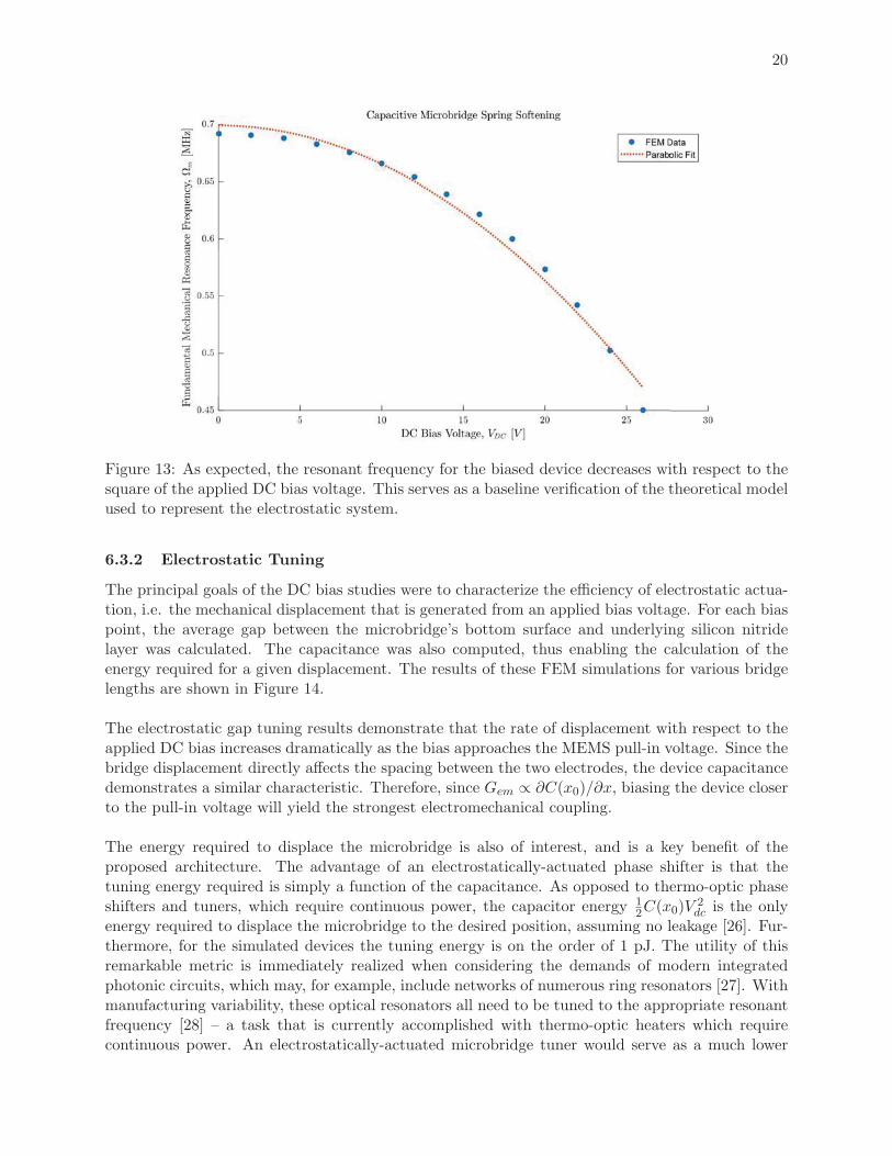
As predicted by Equation 13 in Appendix A, the resonant frequency of the bridge is expected todecrease with respect to the square of the applied DC bias. Comparing the bridge to a simplespring, this decrease in resonance frequency corresponds to a reduced spring constant, or “springsoftening” [51]. The computationally simulated eigenfrequencies at various DC biases, shown inFigure 13, confirms this relationship, and therefore serves as a partial verification of the theoreticalmodel used to derive the device transfer function.
Experimentally, the spring softening effect can also be analyzed for comparison to the computationalresults and to better characterize the overall system.
20
Figure 13: As expected, the resonant frequency for the biased device decreases with respect to thesquare of the applied DC bias voltage. This serves as a baseline verification of the theoretical modelused to represent the electrostatic system.
6.3.2 Electrostatic Tuning
The principal goals of the DC bias studies were to characterize the efficiency of electrostatic actua-tion, i.e. the mechanical displacement that is generated from an applied bias voltage. For each biaspoint, the average gap between the microbridge’s bottom surface and underlying silicon nitridelayer was calculated. The capacitance was also computed, thus enabling the calculation of theenergy required for a given displacement. The results of these FEM simulations for various bridgelengths are shown in Figure 14.
The electrostatic gap tuning results demonstrate that the rate of displacement with respect to theapplied DC bias increases dramatically as the bias approaches the MEMS pull-in voltage. Since thebridge displacement directly affects the spacing between the two electrodes, the device capacitancedemonstrates a similar characteristic. Therefore, since Gem ∝ ∂C(x0)/∂x, biasing the device closerto the pull-in voltage will yield the strongest electromechanical coupling.
The energy required to displace the microbridge is also of interest, and is a key benefit of theproposed architecture. The advantage of an electrostatically-actuated phase shifter is that thetuning energy required is simply a function of the capacitance. As opposed to thermo-optic phaseshifters and tuners, which require continuous power, the capacitor energy 1
2C(x0)V2dc is the only
energy required to displace the microbridge to the desired position, assuming no leakage [26]. Fur-thermore, for the simulated devices the tuning energy is on the order of 1 pJ. The utility of thisremarkable metric is immediately realized when considering the demands of modern integratedphotonic circuits, which may, for example, include networks of numerous ring resonators [27]. Withmanufacturing variability, these optical resonators all need to be tuned to the appropriate resonantfrequency [28] – a task that is currently accomplished with thermo-optic heaters which requirecontinuous power. An electrostatically-actuated microbridge tuner would serve as a much lower

21
Figure 14: DC bias electrostatic actuation study results for various microbridge lengths (shownas different colors). As LMEMS increases, the pull-in voltage (dashed lines) decreases along withthe energy required for a given displacement distance. Capacitance, however, increases due to theincreasing surface area of the electrodes. Fractional change in capacitance versus displacement isapproximately equal, as expected from the constant device geometry.
power alternative, especially for large-scale networks where several tuning elements are required.
The results also indicate that the displacement and capacitance tuning are directly affected by themicrobridge length LMEMS. Due to the increase in mechanical compliance with bridge length, thepull-in voltage decreases with an increasing length. The bridge electrode surface area also increasesfor longer bridges, leading to a larger overall capacitance and a larger change in capacitance asthe bridge is actuated. Despite this increase in capacitance, the energy required to actuate longerbridges decreases due to the decreased bias voltage required for a given displacement. As expected,the fractional capacitance change as a function of displacement is essentially constant regardless ofmicrobridge length.
6.4 Summary
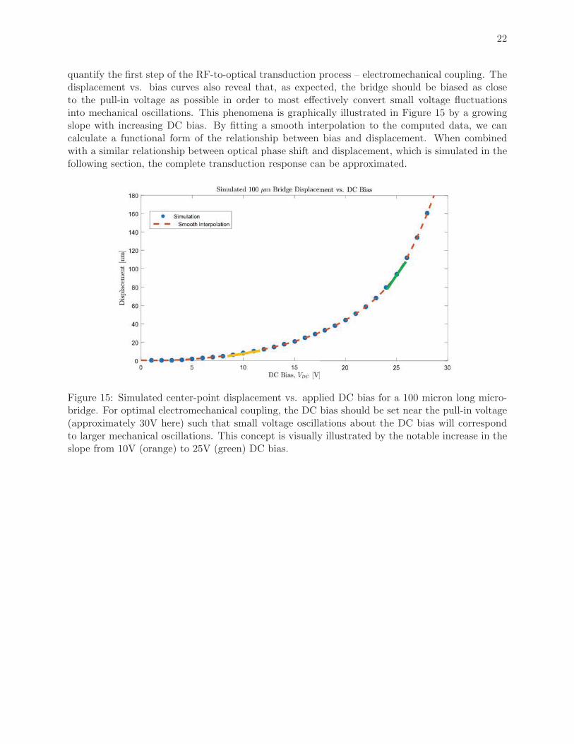
By conducting electromechanical DC bias tests, a mechanical displacement vs. bias curve, similarto that for a 100μm bridge shown in Figure 15, can be simulated. The results of these tests
22
quantify the first step of the RF-to-optical transduction process – electromechanical coupling. Thedisplacement vs. bias curves also reveal that, as expected, the bridge should be biased as closeto the pull-in voltage as possible in order to most effectively convert small voltage fluctuationsinto mechanical oscillations. This phenomena is graphically illustrated in Figure 15 by a growingslope with increasing DC bias. By fitting a smooth interpolation to the computed data, we cancalculate a functional form of the relationship between bias and displacement. When combinedwith a similar relationship between optical phase shift and displacement, which is simulated in thefollowing section, the complete transduction response can be approximated.
Figure 15: Simulated center-point displacement vs. applied DC bias for a 100 micron long micro-bridge. For optimal electromechanical coupling, the DC bias should be set near the pull-in voltage(approximately 30V here) such that small voltage oscillations about the DC bias will correspondto larger mechanical oscillations. This concept is visually illustrated by the notable increase in theslope from 10V (orange) to 25V (green) DC bias.

23
7 Optomechanical Simulation
To quantify the optomechanical coupling parameter Gom ≡ ∂neff/∂x, a series of 2D perturber FEMsimulations were conducted using the geometry depicted in Figure 16. The initial parameters,established to model the experimental devices used in [12], are outlined in Table 1. For eachgeometry tested, the effective index of the fundamental TE mode at 1550 nm was then computedas the microbridge-waveguide gap hMEMS was swept. In an attempt to optimize the effective indextuning performance, the effect of varying several geometric parameters was thoroughly explored.The results of these analysis are listed in Appendix H.
Figure 16: The COMSOL geometry, along with associated dimensions, created for determiningthe optomechanical coupling strength through simulation of the interaction between the suspendedperturber and evanescent field in air.
7.1 2D Perturber Test Results
The simulation results for the default geometry parameters used in the fabricated devices is shown inFigure 17. Since the evanescent field strength of the rib waveguide decays exponentially away fromthe guide, the effective index tuning likewise decays exponentially as the air gap hMEMS betweenthe waveguide and microbridge increases. The resulting effective index tuning range (Δneff > 0.1)considerably exceeds that of common electro-optic modulators [44].
Since the optical phase shift is proportional to the change in effective index (Δφ = 2πλ LMEMSΔneff),
the effective index vs. displacement plot effectively quantifies the performance of the second processrequired for the RF-to-optical transduction scheme – conversion of a microbridge displacement intoan optical phase shift. Note that, similar to the displacement versus bias curve discussed in Section6, the slope of this performance curve increases as the bridge is displaced further into the evanescentfield of the underlying waveguide mode. Therefore, in order to obtain optimal index variations inresponse to a given amplitude of displacement oscillation, the bridge should be displaced as closeas feasible to the underlying waveguide.

24
Figure 17: Simulated effective index tuning performance of the microbridge perturber with thedimensions described in Table 1. The mode profile insets depict increasing capture of the opticalmode within the microbridge as it is lowered from 300 to 100 nm above the underlying waveguide.
Further details on optomechanical simulation and optimization can be found in Section 7 and Ap-pendix H, respectively.

25
8 Expected Performance
By combining the computationally derived voltage-to-displacement transfer function from Section6 with the displacement-to-effective index transfer function (Section 7), the overall transducer re-sponse can be estimated.
First, we can approximate the DC response as
Δφ =2π
λLMEMS [neff(hMEMS|VDC
)− neff(hMEMS|VDC=0)]︸ ︷︷ ︸change in index due to DC displacement
. (4)
At any given DC bias point, the small signal transduction gain – the amplitude of phase oscillationsthat result divided by the amplitude of the input voltage fluctuation – is represented as
δφ
δVs
∣∣∣∣VDC
= transducer gain =
∣∣∣∣Tbare
∣∣∣∣VDC ,ω≈0
. (5)
(a) DC Response (b) Low Frequency Small Signal Response
Figure 18: The predicted DC and low-frequency AC responses of a 100 micron-long microbridge.These responses are found by evaluating the value (DC) or slope (AC) of the electromechanicaland optomechanical coupling performance curves and combining the results in accordance with thedevice transfer function.
These two characteristics are plotted in Figure 18 for the sample 100 micron bridge analyzed inthe previous sections. The DC response on the left hand side, which is essentially a combination ofthe constituent displacement vs. DC bias and effective index vs. displacement plots, demonstratescharacteristics similar to these previous plots. Namely, the slope of the curve increases sharplyas the pull-in voltage is approached. This results from the combination of: 1) the increased dis-placement sensitivity to voltage near the pull-in voltage, and 2) the increased coupling between themicrobridge and evanescent field when the bridge is displaced closer to the underlying waveguide.
The low frequency RF small signal response, or gain curve, shown in Figure 18b is found by eval-uating the slopes – versus the values used for the aforementioned DC phase shift response curve –of the two constituent performance curves at a set DC bias point. The resulting small signal gain,

26
δφ/δVs depicts a similar dependence on DC bias as the previous results.
Due to the mechanical properties of the microbridge, which is characterized by the complex sus-ceptibility factor χ0
m, the small signal gain at RF frequencies cannot be found by simply takingthe derivative of Figure 18a. Instead, the device transfer function must be evaluated. Due to theLorentzian nature of Tbare, the response contains a sharp peak near the mechanical resonance fre-quency Ωm. The width of this peak is described by the mechanical damping coefficient Γm. Figure19 depicts the small signal frequency response of the transducer for the computed 100 micron bridgefundamental resonant frequency of 2.04 MHz and a quality factor Q = Ωm/Γm = 100, a typicalvalue for a microbridge in air [11].2 This result, as with the previous low frequency response curves,is found by substituting the electromechanical and optomechanical response curves into the devicetransfer function.
Figure 19: The RF frequency response of the proposed RF-to-optical transducer for several DCbias voltages (shown in different colors). The small signal gain δφ/δVs has a peak at the mechan-ical resonance frequency of the microbridge, in this case 2.04 MHz. The response is shown on alogarithmic (i.e. decibel or “dB”) scale to avoid having the plot of the resonance dominate theresponse over the rest of the frequency range.
At a DC bias of 25V (close to pull-in), the peak small signal gain is approximately 100 rad/V.The on-resonance half-wave voltage Vπ – a common performance metric which conveys the inputvoltage required to induce an optical phase shift of π – can therefore be calculated as approximately
2The quality factor Q is a commonly used metric when analyzing resonant peaks which relates the rate of oscillationto that of the energy dissipation within the resonator.

27
30 mV, or around two orders of magnitude lower than the same quantity in typical electro-opticand thermo-optic devices [44, 26]. This reduced modulation voltage is one of the key advantagesof this technology; however, it should be noted that the performance advantage is only obtainedwithin the narrow bandwidth of the mechanical resonance. As the quality factor Q of the bridgeincreases, the peak gain also increases, but at the expense of even further narrowing the resonancebandwidth. In other words, the microbridge is characteristic of a very prominent gain-bandwidthtrade-off. Nonetheless, the RF characteristics unveiled in this analysis demonstrate the potentialperformance advantages that can be obtain when only a narrow bandwidth of operation is necessary.
8.1 Summary and Direction
In this section, we presented the results of computational simulations which we conducted andanalyzed. These results serve as a baseline estimate of the performance expected from the pro-posed RF-to-optical transducer. To verify these characteristics and to provide a proof-of-conceptimplementation of the proposed transduction technique, test photonic integrated circuit chips weresubsequently fabricated at the Naval Research Laboratory. In the following section, the fabricationprocess is briefly outlined before analyzing the experimental work conducted with the fabricatedsamples.

28
9 Device Fabrication
In the previously conducted DC analysis of the microbridge phase shifter [12], the MEMS resonatorswere placed above one arm of an integrated interferometer to enable sensitive detection of the phaseshifts introduced by the bridge. This design mirrors the requirements set forth in the RF-to-opticaltransduction architecture discussed in Section 4. Therefore, this design was modified and used forfabrication of new test devices for RF experimentation. The layout file for a sample transduceris depicted in Figure 20. In this layout, a continuous wave laser is coupled to one of two inputwaveguides on the LHS of the image. The narrowed region just to the right of the input, withinwhich the two waveguides are in close proximity to one another, is known as a “directional cou-pler.” Similar to the simple waveguide branch shown for the MZI in Figure 6, a directional couplerenables the controllable division of power from one or two input ports into two output ports. Forthe pursued application, equal 50-50 power splitting between the two output waveguides is desired.Once the input light has been broken into two arms, it propagates to the output direction coupler,where the light is recombined and split between the two output ports. However, before the lightreaches the output directional coupler, the light in the bottom waveguide of the MZI encountersthe MEMS bridge fabricated within the evanescent field of the waveguide. The interaction betweenthe optical signal’s evanescent field and the mechanical microbridge induces a phase shift in thatarm, which is then measured by the interferometer’s output intensity. The two waveguide armsof the interferometer also have a built-in path length imbalance of 100 microns, which enables theoperating point to be tuned by changing the input laser’s wavelength. This tuning capability isa result of an optical path length imbalance which varies as a function of input wavelength overthe fixed physical length imbalance ΔLMZI (an analytic treatment of this feature is detailed withinthe MZI transfer function derivation in Appendix B). The three other bridges illustrated besidethe waveguides are test structures that are used for non-optical testing, such as measurement ofmechanical displacement under an applied DC bias.
Figure 20: The layout of a single test device contains two waveguides of different lengths coupledtogether at the input and output by two directional couplers, thus forming an optical interferometer.Within the interferometer, a 120 micron bridge is placed on the bottom waveguide arm.
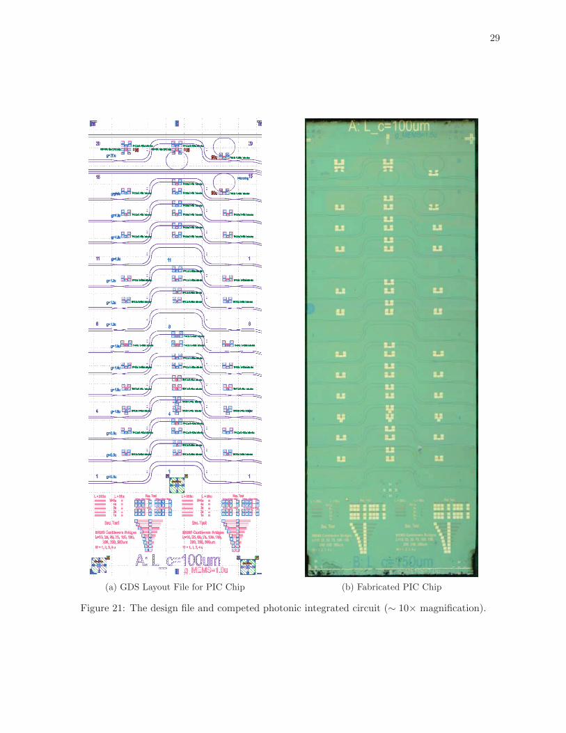
To obtain multiple test devices, the design shown in Figure 20 is tiled vertically until a complete12.5 mm × 5 mm chip is filled. The resulting layout, along with an image of the fabricated chip isshown in Figure 21. The final design is also host to a series of test devices at the bottom of the chipwhich are used to calibrate the fabrication etch times. At the top of the chip, three ring resonatorsare included for future exploration of cavity-assisted readout to improve transduction performance.
The original fabrication run for the previous study leveraged electron beam lithography [48] topattern precision features. In electron beam lithography, an electron beam illuminates regions ofa “photoresist” that are to kept in the fabrication process. Areas exposed to the electron beamdevelop a protective photoresist coating which prevents them from being removed when a subse-
29
(a) GDS Layout File for PIC Chip (b) Fabricated PIC Chip
Figure 21: The design file and competed photonic integrated circuit (∼ 10× magnification).
30
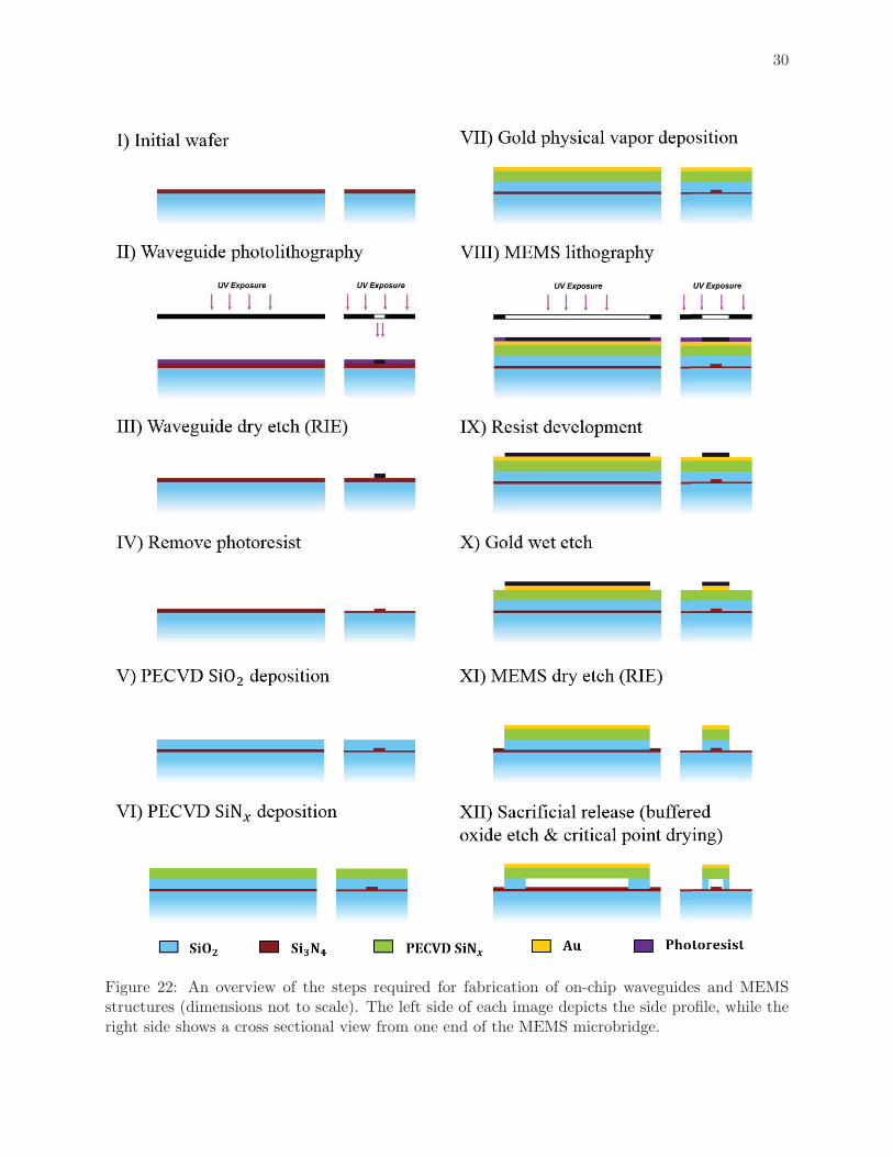
Figure 22: An overview of the steps required for fabrication of on-chip waveguides and MEMSstructures (dimensions not to scale). The left side of each image depicts the side profile, while theright side shows a cross sectional view from one end of the MEMS microbridge.

31
quent etch, or material removal, is conducted. While electron beam lithography affords enhancedresolution for fabricating devices with dimensions smaller than a wavelength of visible light, it isalso slower than traditional techniques since the writing, or scanning, of the electron beam acrossall of the pattern features takes a substantial amount of time. Optical lithography, on the otherhand, exposes the entire pattern of a design at once using a high-intensity UV lamp. A glass“photomask” is placed between the source and the photoresist-coated sample to block light fromareas that are not to be exposed. Similar to electron-beam lithography, the exposed regions arethen considered protected from degradation during future etch steps.
Due to the relative speed of optical lithography, the fabrication process for the samples used in thisstudy was modified to enable its use. This redesign involved the simulation and layout of a newdirectional coupler with larger feature sizes that could be reliably patterned with optical lithog-raphy. The smallest dimension, termed the “critical dimension,” of an optical lithography-baseddesign must typically be on the order of 0.5 microns, approximately one wavelength of UV light, orgreater. By virtue of the lengthening of the interaction region of the directional coupler – the regionwithin which the two waveguides are in close proximity to one another and are able to exchangeenergy – the critical dimension of the design was increased from 0.6 microns to 0.8-1.0 microns.
After laying out the PIC chip photomask with the waveguide and MEMS patterns, the fabrica-tion cycle was commenced. Figure 22 outlines the various steps required to complete the sample.Starting with a silicon nitride on insulator (silicon dioxide) wafer, the interferometer waveguidesare patterned with an MA-6 contact aligner, an industry standard tool for optical lithography. Areactive ion dry etch was then carried out to etch a rib waveguide into the silicon nitride. Afterthe rib waveguides have been fabricated on the sample, a 250 nm layer of oxide is deposited withan Oxford Instruments plasma enhanced chemical vapor deposition (PECVD) tool. This step isfollowed by a similar deposition of 250 nm thick PECVD silicon nitride. A thin 35 nm gold layer,which will eventually form the contact on the top of the MEMS bridge is then sputtered ontothe top of the silicon nitride layer using electron beam physical vapor deposition. Photoresist isspun onto the surface and subsequently patterned with optical lithography using the MEMS layerportion of the photomask. The gold-SiNx-oxide stack is then etched away through a series of wetand dry etches, leaving a microbridge-shaped stack of gold and silicon nitride supported on top ofoxide. This oxide lying beneath the portion of the bridge to be suspended is known as the sacrificialoxide – it is etched away with a timed buffered oxide etch to leave the silicon nitride microbridgesuspended above two oxide anchors (these anchors are preserved during the oxide etch, with is timelimited to prevent significant undercut of these supports). To complete the fabrication cycle, thesample is dried in a critical point dryer [49], an instrument which leverages the controlled phasetransition of liquid CO2 to avoid the destructive adhesive forces involved with regular drying thattend to collapse microbridges.

32
Figure 23: A height profile of a typical microbridge collected with a white light optical profilometer.The color represents the height above the surface (blue). A precise measurement of this structureyields a post height of approximately 500 nm, which is expected after the deposition of 250 nm ofoxide and 250 nm of silicon nitride.
Using a Zygo optical profilometer, the height profile of various microbridges was collected. Oneexample, which depicts a taut bridge suspended between four supports, is shown in Figure 23. Twosupports on either side of the bridge are required to suspend the microbridge without interferingwith the underlying waveguide which runs along the channel parallel to the microbridge.

33
10 Experimental Design and Methodology
To validate the results of the computational characterization provided in Section 8, the dependenceof the fabricated device’s response upon input RF signal frequency, RF power, and DC bias voltagewas experimentally determined. An experimental apparatus, shown in Figure 24, was first designedand constructed to enable complete parametric control of the transducer. Namely, the setup wasdesigned to allow for variation in the wavelength of light input into the system, the DC bias appliedacross the microbridge, as well as the frequency and amplitude of the RF input signal.
Figure 24: An overview of the experimental apparatus constructed to study the fabricated testdevices. The setup features a composite DC+RF voltage which can be placed across the microbridgeto drive the system. By connecting the RF output of a vector network analyzer to the microbridgeand the interferometer’s output photodetector to the network analyzer’s input, the system responsecan be determined as a function of frequency.
The photonic integrated circuit (photograph in Figure 25) was placed on a translation stage foralignment purposes. An input lensed fiber connected to a tunable laser was edge-coupled (Figure26) to an input port of an on-chip interferometer. A second lensed fiber was connected between theinterferometer output and a photodetector which included an in-house developed transimpedanceamplifier. The photodetector’s frequency response, which is indicative of a detection bandwidth of∼5 MHz, is shown in Figure 27. Shielded probes on micrometered stages are used to apply theelectrical input signal across the microbridge, as depicted in Figure 28.
The probes are connected to a shielded SMA cable which is in turn linked to the output of a biastee, which combines input DC and RF stimuli onto a common signal. The DC input of the biastee is driven by a benchtop Keithley 2400 DC power supply. This source is shunted with a 50kΩterminator for stabilization. The tee’s RF input is connected through a 50Ω in-line termination(for proper impedance matching between the source and load) to the RF stimulus from a vectornetwork analyzer. The network analyzer response is provided by the photodetector output, which

34
is connected in parallel to a benchtop digital multimeter for visualization of the DC photodetectoroutput level.
Figure 25: An image of the photonic integrated circuit with input and output lensed fibers coupledto the respective on-chip interferometer ports. Micrometered probes, monitored under a microscope(red objective) connected to a live video feed, are used to connect to the bridge electrodes in order toactuate the devices. The probes are encased in aluminum foil to avoid coupling unwanted ambientnoise into the measurement.
Figure 26: A video-captured image of the lensed fiber coupled to an input port of an on-chip MZI.

35
Figure 27: The photodetector frequency response for a 1550 nm laser with varying power. A cornerfrequency of the transimpedance amplifier is readily apparent at approximately 5 MHz; beyond thisfrequency, the detector response rapidly drops off at approximately 40 dB/decade, thus indicatingthe presence of a second-order low-pass filter.
Figure 28: A video-captured image of the probes connected across the actuation electrodes for themicrobridge. The RHS probe is connected to ground, while the LHS is the positive voltage source.

36
11 Experimental Results and Analysis
Before biasing any of the bridges, baseline spectra of each interferometer were taken by varyingthe input wavelength of the tunable laser source. Given a constant path length imbalance of 100microns between the two arms, the varying wavelength corresponds to a change in optical phaseshift between the arms (see Section 4), thus yielding a sinusoidal, wavelength-dependent outputintensity spectrum. Due to the four-port directional couplers at the input and output of each inter-ferometer, there are four possible measurement combinations (explained in Figure 29) from whichthis spectrum can be collected.
Figure 29: The on-chip Mach-Zehnder interferometers (MZIs) are constructed with two 2×2 di-rectional couplers instead of simple “Y-branches.” Therefore, four possible optical spectra can beobtained from the device due to the four combinations of input and output ports. If the outputsignal is measured from the waveguide that it is launched into, the output port is denoted BAR n,where n is the input port. Otherwise, if the output is taken from the opposite arm than the onewhich it was launched in, it is noted as the CROSS n. Note that physical pathlength differencebetween the two arms is ΔLMZI.
Two obtained spectra are shown in Figure 30. Although the two devices have the same inter-ferometer design (neglecting any manufacturing variability), one device is a bare MZI, while theother is an MZI with a 90 micron bridge coupled to one arm of the interferometer. The periodicnature expected from the MZI transfer function (Appendix B) is readily apparent for each, andindicates a period, or free spectral range (FSR), on the order of 10 nm. The extinction ratio, orratio between maximum and minimum power, achieves a peak value of nearly 25 dB for the CROSSB measurement, indicating ideal power splitting by the input and output directional couplers. Asderived in Appendix B, the change in FSR is expected from bridge-induced phase shifts, and canbe used to calculate the change in effective index within the region where the bridge is interactingwith the optical signal. The simple relations (Appendix B)
ng =λ2
ΔLMZI(FSR)Δneff =
ΔLMZIΔng
LMEMS, (6)
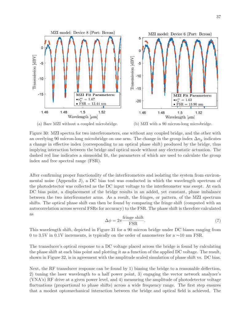
where λ is the laser wavelength in the medium and ΔLMEMS is the intrinsic path length mismatchwithin the MZI, can be combined to estimate the change in index by the 90 micron bridge to be onthe order of 0.05. This value is in agreement with that expected from the simulated effective indexvs. displacement curve, and also demonstrates that the microbridge is placed within the opticalmode with non-zero optomechanical coupling.
37
(a) Bare MZI without a coupled microbridge. (b) MZI with a 90 micron-long microbridge.
Figure 30: MZI spectra for two interferometers, one without any coupled bridge, and the other withan overlying 90 micron-long microbridge on one arm. The change in the group index Δng indicatesa change in effective index (corresponding to an optical phase shift) produced by the bridge, thusimplying interaction between the bridge and optical mode without any electrostatic actuation. Thedashed red line indicates a sinusoidal fit, the parameters of which are used to calculate the groupindex and free spectral range (FSR).
After confirming proper functionality of the interferometers and isolating the system from environ-mental noise (Appendix J), a DC bias test was conducted in which the wavelength spectrum ofthe photodetector was collected as the DC input voltage to the interferometer was swept. At eachDC bias point, a displacement of the bridge results in an added, yet constant, phase imbalancebetween the two interferometer arms. As a result, the fringes, or pattern, of the MZI spectrumshifts. The optical phase shift can then be found by comparing the fringe shift (computed with anautocorrelation across several FSRs for accuracy) to the FSR. The phase shift is therefore calculatedas
Δφ = 2πfringe shift
FSR. (7)
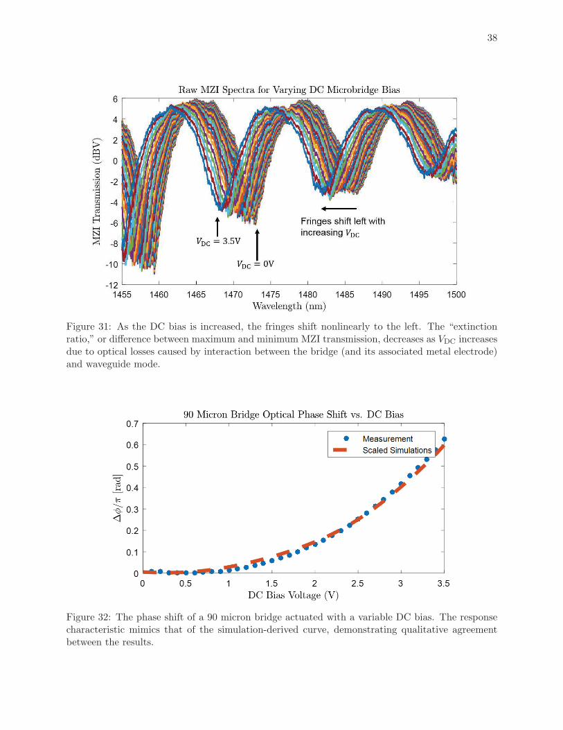
This wavelength shift, depicted in Figure 31 for a 90 micron bridge under DC biases ranging from0 to 3.5V in 0.1V increments, is typically on the order of nanometers for a ∼10 nm FSR.
The transducer’s optical response to a DC voltage placed across the bridge is found by calculatingthe phase shift at each bias point and plotting it as a function of the applied DC voltage. The result,shown in Figure 32, is in agreement with the amplitude scaled simulation of phase shift vs. DC bias.
Next, the RF transducer response can be found by 1) biasing the bridge to a reasonable deflection,2) tuning the laser wavelength to a half power point, 3) engaging the vector network analyzer’s(VNA’s) RF drive at a given power level, and 4) measuring the amplitude of photodetector voltagefluctuations (proportional to phase shifts) across a wide frequency range. The first step ensuresthat a modest optomechanical interaction between the bridge and optical field is achieved. The
38
Figure 31: As the DC bias is increased, the fringes shift nonlinearly to the left. The “extinctionratio,” or difference between maximum and minimum MZI transmission, decreases as VDC increasesdue to optical losses caused by interaction between the bridge (and its associated metal electrode)and waveguide mode.
Figure 32: The phase shift of a 90 micron bridge actuated with a variable DC bias. The responsecharacteristic mimics that of the simulation-derived curve, demonstrating qualitative agreementbetween the results.
39
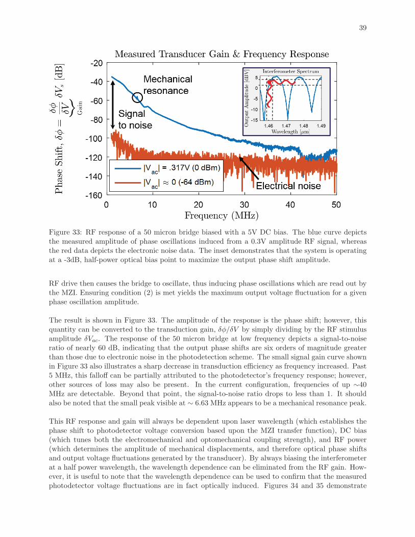
Figure 33: RF response of a 50 micron bridge biased with a 5V DC bias. The blue curve depictsthe measured amplitude of phase oscillations induced from a 0.3V amplitude RF signal, whereasthe red data depicts the electronic noise data. The inset demonstrates that the system is operatingat a -3dB, half-power optical bias point to maximize the output phase shift amplitude.
RF drive then causes the bridge to oscillate, thus inducing phase oscillations which are read out bythe MZI. Ensuring condition (2) is met yields the maximum output voltage fluctuation for a givenphase oscillation amplitude.
The result is shown in Figure 33. The amplitude of the response is the phase shift; however, thisquantity can be converted to the transduction gain, δφ/δV by simply dividing by the RF stimulusamplitude δVac. The response of the 50 micron bridge at low frequency depicts a signal-to-noiseratio of nearly 60 dB, indicating that the output phase shifts are six orders of magnitude greaterthan those due to electronic noise in the photodetection scheme. The small signal gain curve shownin Figure 33 also illustrates a sharp decrease in transduction efficiency as frequency increased. Past5 MHz, this falloff can be partially attributed to the photodetector’s frequency response; however,other sources of loss may also be present. In the current configuration, frequencies of up ∼40MHz are detectable. Beyond that point, the signal-to-noise ratio drops to less than 1. It shouldalso be noted that the small peak visible at ∼ 6.63 MHz appears to be a mechanical resonance peak.
This RF response and gain will always be dependent upon laser wavelength (which establishes thephase shift to photodetector voltage conversion based upon the MZI transfer function), DC bias(which tunes both the electromechanical and optomechanical coupling strength), and RF power(which determines the amplitude of mechanical displacements, and therefore optical phase shiftsand output voltage fluctuations generated by the transducer). By always biasing the interferometerat a half power wavelength, the wavelength dependence can be eliminated from the RF gain. How-ever, it is useful to note that the wavelength dependence can be used to confirm that the measuredphotodetector voltage fluctuations are in fact optically induced. Figures 34 and 35 demonstrate

40
this phenomenon.
Figure 34: The intensity vs. wavelength spectrum for a sample interferometer with a 90 micronmicrobridge. The red points depict the bias points to which the laser was tuned to ensure that theoutput fluctuations were the result of changes in optical phase.
Figure 35: As expected, -3dB bias points have the maximum output amplitude, while peaks andtroughs of the intensity vs. wavelength spectrum yield a minimal output. Furthermore, the 180 de-gree phase difference depicted between bias points on opposite sides of the peak intensity wavelengtheven further illustrates the connection between input voltage and output optical phase fluctuations.

41
By tuning the wavelength to different bias points across the interferometer intensity vs. wavelengthspectrum, the amplitude of the output voltage fluctuations should be maximized at half-powerpoints and minimized at peaks and troughs. Figure 34 depicts one period of a 90 micron bridgeinterferometer’s spectrum when biased with a 2.2V DC bias. The red points indicate bias points atwhich the response amplitude and phase were recorded about the mechanical resonant frequency at6.63 MHz. These responses are shown in Figure 35. As expected, the amplitude of the response ismaximized at the two -3dB half-power points, obtains an intermediate value at the -2.2 dB values(due to the non-maximized value of the slope of the intensity vs. wavelength curve at that point),and is minimized to nearly zero at both the peak and trough. Furthermore, the responses on op-posite sides of the peak intensity value, where the slopes are negatives of one another, are out ofphase by 180 degrees – a direct reflection of this slope reversal. Therefore, the wavelength tuningconfirms via both amplitude and phase that the output voltage fluctuations are in fact opticallyinduced.
Even when always biased to a half power point in order to maximize phase shift to output in-tensity transduction performance, the induced phase shift will always depend on the RF powerof the drive tone as well as the DC bias applied across the microbridge. As a final experimentaltest, the amplitude of phase shifts is mapped as a function of these two variables. The mechanicalresonance peak at 6.63 MHz presents itself as an ideal location from which to track this dependence.
Figure 36: The transduced amplitude and phase for a 50 micron bridge biased at 5.5V and drivenat varying RF powers. The black dotted lines represent Lorentzian curves fitted to each resonantpeak.
Figure 36 demonstrates how data points were collected for the test. A set DC bias was applied tothe bridge, and the RF amplitude was subsequently varied. This process was iterated as the DCbias was slowly incremented. The peak value of each curve was selected and plotted on Figure 37.Figure 37 depicts the expected dependency upon RF drive amplitude and DC bias. Due to thelinear first order Taylor expansion of the MZI spectrum at the half-power point, increases in RF
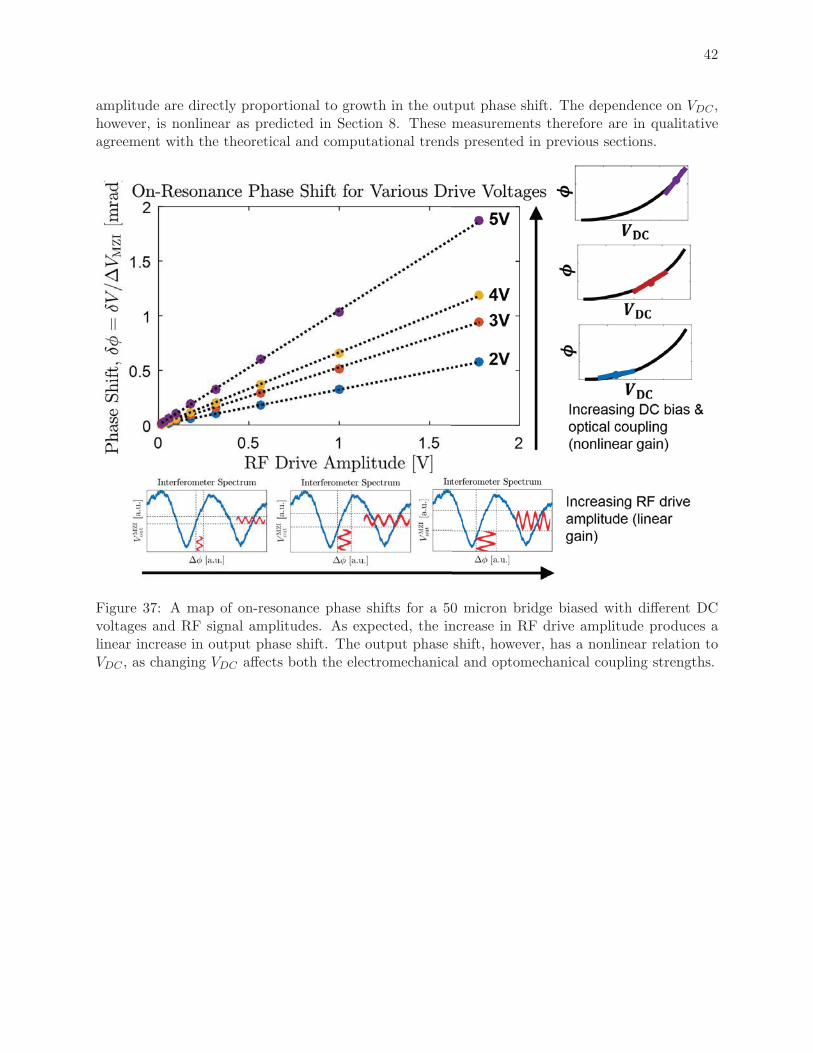
42
amplitude are directly proportional to growth in the output phase shift. The dependence on VDC ,however, is nonlinear as predicted in Section 8. These measurements therefore are in qualitativeagreement with the theoretical and computational trends presented in previous sections.
Figure 37: A map of on-resonance phase shifts for a 50 micron bridge biased with different DCvoltages and RF signal amplitudes. As expected, the increase in RF drive amplitude produces alinear increase in output phase shift. The output phase shift, however, has a nonlinear relation toVDC , as changing VDC affects both the electromechanical and optomechanical coupling strengths.

43
12 Discussion and Future Work
While the majority of the experimental data trends, including the phase shift vs. DC bias, theeffect of varying the interferometer’s optical bias point, and the effect of increasing the amplitude ofRF signal applied across the bridge, are in direct correspondence with the theoretical and compu-tational predictions, some rifts still remain. Notably, the narrow, large-amplitude resonant peakscharacteristic of the Lorentz functions simulated in Figure 19 are absent from the experimentallydetermined RF device response. A rapid gain drop-off for frequencies lower than that of the studiedresonant peak is also depicted in Figure 33, while the amplitude of the theoretical transfer functionis constant for frequencies lower than the resonant frequency. This performance decay at highfrequencies can be partially attributed to the narrow bandwidth of the photodetector; however,considering the loss is evident well before the photodetector corner frequency, other loss mecha-nisms must be present in addition. In the future, a complete analysis of electrical, mechanical, andoptical noise sources would contribute to a more accurate estimate of the expected device sensitivity.
To investigate these discrepancies and to further explore the experimental limits of the transducer’sperformance, future testing could be conducted with the photonic integrated circuit placed withina vacuum chamber. Doing so would minimize the effects of viscous damping, thereby increasingthe quality factor of the mechanical microbridge [10]. This increase in Q may make the mechanicalresonant peaks more readily visible in the RF response spectrum. Furthermore, the reduced bridgedamping may also enable bridge displacements from thermal energy alone – in absence of any ex-ternal electronic stimulus – to be detected. If so, this spectrum would enable a critical calibrationof the optomechanical transduction’s displacement sensitivity [50].
Once in vacuum, the microbridges can also be capacitively coupled to an external high-Q LC circuitto not only improve the electromechanical coupling performance, but to study the rich dynamicsof strongly coupled electronic and mechanical oscillators [4].
Both of these extensions would aid in further connecting the theoretical work presented within thisstudy to the device’s experimental behavior – all while affording new environments within whichthe proposed electro-opto-mechanical RF-to-optical transduction technique could be evaluated.
44
13 Conclusions
This report details an extensive study of a novel, fully integrated method for RF-to-optical trans-duction in which a mechanical microbridge resonator placed within an integrated photonic circuitcouples electronic and optical signals. After deriving a theoretical transfer function to characterizethe transduction architecture, computational simulations were created to determine the efficiencyof each step of the electro-opto-mechanical transduction process. To test the predictive reliability ofour modeling and simulation results, we fabricated test devices at the Naval Research Laboratoryand conducted a series of characterization tests to compare actual performance to our theoreticalpredictions. These tests validated the mechanical, optomechanical, and electromechanical func-tional blocks of our model and confirmed our understanding of the device behavior.
While the experimental portion of this research focused on investigating the first revision of thetransducer, the potential for future optimization and improvement of the system was also presented.The design space of the transducer, including coupling techniques, physical parameters, and devicegeometries, was characterized, yielding optimum coupling conditions that bound the device’s peakperformance. Feasible experimental directions, such as the incorporation of a coupled electrical os-cillator to improve electromechanical coupling, the variation of waveguide parameters to maximizeoptomechanical coupling, and the encapsulation of the microbridge in vacuum to reduce damping,were not only proposed, but also evaluated to estimate their effect on overall system performance.
The proposed technique is host to unique properties which may be advantageous to future appli-cations. Notably, the transduction architecture enables complete integration into a single designwhich can be fabricated with common microelectronic techniques. The electrostatic actuation in-volved also enables low-power conversion of radio frequency signals. If actuated at a mechanicalresonance frequency, our modeling demonstrates that the resulting transduction gain can drasticallyexceed that of common electro-optic and thermo-optic transducers. This enhanced performance,however, is only obtained within the narrow mechanical resonance bandwidth and at the low reso-nant frequencies of the bridge, which are on the order of 1-10 MHz. Depending upon the particularapplication, the drawbacks may be acceptable or even inconsequential when compared to the ad-vantages. Thus, the results of this comprehensive study not only validate the potential for futuredevelopment of the technology, but also add to the growing body of knowledge regarding electro-opto-mechanical transduction techniques.
In general, the use of mechanical structures to efficiently mediate conversion between radio fre-quency and optical signals has recently ignited widespread research interest due to the potentialuse of such transducers to solve a diverse set of technical challenges in fields ranging from sensingto quantum information science. An ideal transducer, for example, would enable the long-distance,low-noise detection and transmission of weak radio frequency signals – signals which would havebeen lost or hidden below thermal noise in traditional electronic systems. Before the complete realmof possible applications can be envisioned, however, the enabling technologies of such transducersmust be fully explored and characterized. This research marks one step towards that end.
45
References
[1] Taylor, J. M., Sørensen, A. S., Marcus, C. M. & Polzik, E. S., Laser cooling and opticaldetection of excitations in a LC electrical circuit. Physical Review Letters 107, 273601 (2011).
[2] Pruessner, M. W., et. al., An Opto-Electro-Mechanical Phase Shifter. Proceedings from the2015 CLEO Conference.
[3] Aspelmeyer, M., Kippenberg, T.J. & Marquardt, F., Cavity optomechanics. Reviews of Mod-ern Physics 86, 1392-1452 (2014).
[4] Bagci, T., et. al., Optical detection of radio waves through a nanomechanical transducer.Nature 507, 81-85 (2014).
[5] Bochmann, J., Vainsencher, A., Awschalom, D. D. & Cleland, A. N., Nanomechanical cou-pling between microwave and optical photons. Nat. Phys. 9, 712-716 (2013).
[6] Andrews, R. W. et al., Bidirectional and efficient conversion between microwave and opticallight. Nat. Phys. 10, 321-326 (2014).
[7] Kraus, J.D., Radio Astronomy (McGraw, 1966).
[8] DARPA Optical Radiation Cooling and Heating in IntegratedDevices (ORCHID) Program. http://www.darpa.mil/program/
optical-radiation-cooling-and-heating-in-integrated-devices.
[9] DARPA Quantum-Assisted Sensing and Readout (QuASAR) Program. http://www.darpa.mil/program/quantum-assisted-sensing-and-readout.
[10] Cleland, A.N., Foundations of Nanomechanics: from solid state theory to device applications.Springer, Berlin (2010).
[11] Pruessner, M. W., et. al., An Optomechanical Transducer Platform for Evanescent FieldDisplacement Sensing. IEEE Sensors Journal 14, 3473-3481 (2014).
[12] Pruessner, M., et. al., Broadband opto-electro-mechanical effective refractive index tuning ona chip. Optics Express 24 13917-13930 (2016).
[13] Chrostowski, L. & Hochberg, M., Silicon Photonics Design (Cabridge University Press, 2015).
[14] Aspelmeyer, M., Kippenberg, T.J., & Marquardt, F., Cavity optomechanics. Rev. Mod. Phys.86, (2014).
[15] Garrido Alzar, C. L., Martinez, M. A. G. & Nussenzveig, P., Classical analog of electromag-netically induced transparency. Am. J. Phys. 70, 37-41 (2002).
[16] Novotny, L., Strong coupling, energy splitting, and level crossings: A classical perspective.Am. J. Phys. 78, 1199-1202 (2010).
[17] Palais, J. C., Fiber Optic Communications 4th ed.. Pearson Prentice Hall, New Jersey (2005).
[18] MIT 6.777J Material Property Database – PECVD Silicon Nitride. www.mit.edu/~6.777/matprops/pecvd_sin.htm.
46
[19] Lehnert, K.W. in Cavity Optomechanics (Aspelmeyer, M., Kippenberg, T.J., & Marquardt,F. ed.), 233-252 (Springer, 2014).
[20] Regal, C. A. & Lehnert, K. W., From cavity electromechanics to cavity optomechanics. J.Phys. Conf. Ser 264, (2011).
[21] COMSOL Multiphysics, www.comsol.com.
[22] Unterreithmeier, Quirin P., Weig, Eva M., Kotthaus, J. P., Universal transduction schemefor nanomechanical systems based on dielectric forces. Nature 458, 1001-1004 (2009).
[23] Schmid, S., Hierold, C. & Boisen, A., Modeling the Kelvin polarization force actuation ofmicro and nanomechanical systems. J. Appl. Phys. 107, (2010).
[24] Southworth, D. R. et al., Stress and silicon nitride: A crack in the universal dissipation ofglasses. Phys. Rev. Lett. (2009).
[25] Zhang, W., et. al., Electrostatic pull-in instability in MEMS/NEMS: A review. Sensors andActuators 214, (2014).
[26] Harris, N.C., et. al., Efficient, compact and low loss thermo-optic phase shifter in silicon.Optics Express 22, (2014).
[27] Bogaerts, W., et. al., Silicon microring resonators, Laser Photonics Rev. 6, (2012).
[28] Li, G., et. al., 25Gb/s 1V-driving CMOS ring modulator with integrated thermal tuning.Optics Express 19, 20435-20443(2011).
[29] Teufel, J. D. et al., Circuit cavity electromechanics in the strong-coupling regime. Nature471, 204-208 (2011).
[30] Bagci, T., Opto-Electromechanical Devices for Low-Noise Detection of Radio Waves. Univer-sity of Copenhagen PhD Thesis, (2014)
[31] Zalevsky, Z., Integrated micro- and nanophotonic dynamic devices: a review. Journal ofNanophotonics 1, 012504-012504-24 (2007).
[32] Kippenberg, T.J. & Vahala, K. J., Cavity optomechanics: back-action at the mesoscale.Science 321, 1172-1176 (2008).
[33] Regal, C. A. & Lehnert, K. W., From cavity electromechanics to cavity optomechanics. J.Phys. Conf. Ser. 264, 012025-012025-8 (2011).
[34] Safavi-Naeini, A. H. & Painter, O., Proposal for an optomechanical traveling wave phonon-photon translator. New J. Phys. 13, 013017-013017-30 (2011).
[35] Bochmann, J., Vainsencher, A., Awschalom, D. D. & Cleland, A. N., Nanomechanical cou-pling between microwave and optical photons. Nature Phys. 9, 712-716 (2013).
[36] Devgan, P. S., Pruessner, M. W., Urick, V. J. & Williams, K. J., Detecting low-power andRF signals and using a multimode optoelectronic and oscillator and integrated optical filter.IEEE Photonics Technol. Lett. 22, 152-154 (2010).
[37] Ilchenko, V. S. et al., Ka-band all-resonant photonic microwave receiver. IEEE PhotonicsTechnol. Lett. 20, 1600-1612 (2008).

47
[38] Kolpekwar, A., Blanton, R.D., & Woodilla, D., Failure Modes for Stiction in Surface-Micromachined MEMS. 1998 IEEE International Test Conference Proceedings, 551-556.
[39] Mastrangelo, C.H., Adhesion-Related Failure Mechanisms in Micomechanical Devices. Tri-bology Letters 3, 223-238 (1997).
[40] Savkar, A.A, et. al., On the Use of Structural Vibrations to Release Stiction Failed MEMS.Journal of Microelectromechanical Systems 16, 163-173 (2007).
[41] Gupta, V., et. al., Recovery of Stiction-Failed MEMS Structures Using Laser-Induced StressWaves. Journal of Microelectromechanical Systems 13, 696-700 (2004).
[42] Leseman, Z.C., Koppaka, S., & Mackin, T.J., A Fracture Mechanics Description of StressWave Repair in Stiction-Failed Microcantilevers: Theory and Experiments. Journal of Mi-croelectromechanical Systems 16, 904-911 (2007).
[43] Stievater, T.H., et. al., Suspended photonic waveguide devices. Applied Optics 54, 164-173(2015).
[44] Lipson, M., Compact Electro-Optic Modulators on a Silicon Chip. IEEE Journal of SelectedTopics in Quantum Electronics 12, 1520-1526 (2006).
[45] Quigley, G.R., Harris, R.D., Wilkinson, J.S., Sensitivity enhancement of integrated opticalsensors by use of thin high-index films. Applied Optics 38, 6036-6039 (1999).
[46] Hahn, J., et. al. Measurement of the enhanced evanescent fields of integrated waveguides foroptical near-field sensing. Applied Optics 47, 2357-2360 (2008).
[47] Najafi, K., & Suzuki, K. A Novel Technique and Structure for the Measurement of InstrinsicStress and Young’s Modulus of Thin Films. IEEE Micro Electro Mechanical Systems Proceed-ings, An Investigation of Micro Structures, Sensors, Actuators, Machines and Robots, 96-97(1989).
[48] Tseng, A.A., et. al. Electron Beam Lithography in Nanoscale Fabrication: Recent Develop-ment. IEEE Transactions on Electronics Packing Manufacturing 26, 141-149 (2003).
[49] Jafri, I.H., Busta, H., Walsh, S.T. Critical point drying and cleaning for MEMS technology.SPIE MEMS Reliability for Critical and Space Applications 3880, 51-58. (1999).
[50] Li, M., et. al. Harnessing optical forces in integrated photonic circuits. Nature 456, 480-485(2008).
[51] Kozinsky, I., Postma, H.W. Ch., Bargatin, I., & Roukes, M.L., Tuning nonlinearity, dy-namic range, and frequency of nanomechanical resonators. Applied Physics Letters 88, 253101(2006).
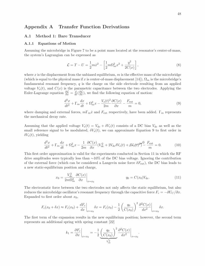
48
Appendix A Transfer Function Derivations
A.1 Method 1: Bare Transducer
A.1.1 Equations of Motion
Assuming the microbridge in Figure 7 to be a point mass located at the resonator’s center-of-mass,the system’s Lagrangian can be expressed as
L = T − U =1
2mx2 −
[1
2mΩ2
mx2 +q2
2C(x)
], (8)
where x is the displacement from the unbiased equilibrium,m is the effective mass of the microbridge(which is equal to the physical mass if x is center-of-mass displacement [14]), Ωm is the microbridge’sfundamental resonant frequency, q is the charge on the side electrode resulting from an appliedvoltage Vs(t), and C(x) is the parametric capacitance between the two electrodes. Applying theEuler-Lagrange equation ∂L
∂x = ddt(
∂L∂x ), we find the following equation of motion:
d2x
dt2+ Γm
dx
dt+Ω2
mx− Vs(t)2
2m
∂C(x)
∂x− Fext
m= 0, (9)
where damping and external forces, mΓmx and Fext respectively, have been added. Γm representsthe mechanical decay rate.
Assuming that the applied voltage Vs(t) = Vdc + δVs(t) consists of a DC bias Vdc as well as thesmall reference signal to be modulated, δVs(t), we can approximate Equation 9 to first order inδVs(t), yielding
d2x
dt2+ Γm
dx
dt+Ω2
mx− 1
2m
∂C(x)
∂x(V 2
dc + 2VdcδVs(t) +�����0δVs(t)
2)− Fext
m= 0. (10)
This first order approximation is valid for the experiments conducted in Section 11 in which the RFdrive amplitudes were typically less than ∼10% of the DC bias voltage. Ignoring the contributionof the external force (which can be considered a Langevin noise force δFext), the DC bias leads toa new static-equilibrium position and charge,
x0 =V 2dc
2mΩ2m
∂C(x)
∂x
∣∣∣∣x=x0
q0 = C(x0)Vdc. (11)
The electrostatic force between the two electrodes not only affects the static equilibrium, but alsoreduces the microbridge oscillator’s resonant frequency through the capacitive force Fc = −∂UC/∂x.Expanded to first order about x0,
Fc(x0 + δx) ≈ Fc(x0) +dFc
dx
∣∣∣∣x=x0
δx = Fc(x0)− 1
2
(q0
C(x0)
)2 ∂2C(x)
dx2
∣∣∣∣x=x0
δx.
The first term of the expansion results in the new equilibrium position; however, the second termrepresents an additional spring with spring constant [22]
k1 =∂Fc
∂x
∣∣∣∣x=x0
= −12
(q0
C(x0)
)2
︸ ︷︷ ︸V 2dc
∂2C(x)
dx2
∣∣∣∣x=x0
.

49
The total effective spring constant for the parallel springs is thus k = k0 + k1 = mΩ2m, where
k0 = mΩ2m and Ωm represents the capacitively-softened [51] resonant frequency. The resulting
reduced mechanical resonance frequency is
Ωm =
√k0m− 1
2m
(q0
C(x0)
)2 ∂2C(x)
dx2
∣∣∣∣x=x0
≈ Ωm
(1− 1
4k0
(q0
C(x0)
)2 ∂2C(x)
∂x2
∣∣∣∣x=x0
), (12)
thus representing a change in frequency of
ΔΩm = Ωm − Ωm = −Ωm
4k0
(q0
C(x0)
)2 ∂2C(x)
∂x2
∣∣∣∣x=x0
= − V 2dc
4mΩm
∂2C(x)
∂x2
∣∣∣∣x=x0
. (13)
This frequency shift is immediately realized upon linearizing the system’s equation of motion aboutthe equilibrium position. From Equation 10, the response to first order perturbations can be writtenas
d2δx
dt2+ Γm
dδx
dt+
⎛⎜⎜⎜⎝Ω2m−
V 2dc
2m
∂2C(x)
∂2x
∣∣∣∣x=x0︸ ︷︷ ︸
2ΩmΔΩm
⎞⎟⎟⎟⎠ δx− Vdc
m
∂C(x)
∂xδVs(t)− δFext
m= 0. (14)
Assuming that the quantity (ΔΩm)2 is negligible,
d2δx
dt2+ Γm
dδx
dt+ Ω2
mδx− Vdc
m
∂C(x)
∂xδVs(t)− δFext
m= 0. (15)
Equation 15 is readily solved in frequency space. After taking the Fourier transform, we find
−ω2δX(jω)− jωΓmδX(jω) + Ω2mδX(jω)− Vdc
m
∂C(x)
∂xδVs(jω)− δFext(jω)
m= 0 . (16)
For notational convenience, note that the resonant frequency Ωm has been redefined to equal thereduced resonant frequency (i.e. Ωm = Ωm). In Equation 16, and throughout the paper, we haveused the e−jωt convention, and denote Fourier transform pairs as X(jω)⇔ x(t).
A.1.2 Signal Readout
For the bare system without an integrated LC resonator, the application of an external force orbias voltage results in a mechanical displacement as well as a corresponding optical phase shift.Therefore, the transduction performance can be analyzed by considering both mechanical and op-tical readouts.
Assuming the applied bias signal dominates the response of the system, the resulting electromechan-ical transfer function, which defines the mechanical motion in response to an electrical excitation,is
δX(jω)
δVs(jω)=
Vdc
m(Ω2m − ω2 − jωΓm)
∂C(x)
∂x
∣∣∣∣x=x0
= Vdcχ0m
∂C(x)
∂x
∣∣∣∣x=x0
, (17)
where χ0m ≡ δX(jω)
δFext(jω)
∣∣∣∣δVs=0
= 1m(Ω2
m−ω2−jωΓm)is the mechanical susceptibility for the external force-
dominated system where δVs is negligible.

50
The displacement-induced interaction with a weakly-confined waveguide mode results in optome-chanical transduction which modifies the overall system gain. The optomechanical system consiststhe mechanical oscillator placed horizontally above a parallel underlying waveguide. Displacementsof the mechanical resonator result in a controllable interaction with the large evanescent field of thewaveguide, which changes the waveguide’s effective index of refraction neff(x) as a function of thevertical displacement x along the horizontal length of the resonator. For a phase shifter mountedin a Mach-Zehnder interferometer (MZI) [17], the resulting optical phase shift can be written as[12]
Δφ = kLMEMSΔneff(x), (18)
where k = 2π/λ is the wave number, LMEMS is the horizontal length of the resonator, and x is thevertical displacement from hMEMS, the average gap between the waveguide and overlying resonator.To first order, the effective index can be approximated as
neff(x0 + δx) = neff(hMEMS) +∂neff
∂x
∣∣x0=hMEMS
δx︸ ︷︷ ︸Δneff
= neff(hMEMS) +Gomδx. (19)
Here, we have defined the optomechanical coupling parameter Gom ≡ ∂neff/∂x∣∣x0=hMEMS
. The rela-tionship between x, the equilibrium displacement, and hMEMS, the average microbridge-waveguidegap, is clarified in Figure 7.
The overall device transfer function is simply the product of those for the electromechanical andoptomechanical systems:
Tbare =δΦ(jω)
δVs(jω)=2π
λVdcχ
0mLMEMSGom
∂C(x)
∂x
∣∣∣∣x=x0
. (20)
A.2 Method II: LC Coupled System
A.2.1 Equation of Motion – DC Biased
Following the procedure and analysis technique proposed in [4], an alternative Lagrangian derivationcan be implemented to determine the transducer’s equations of motion. The Lagrangian [19] forthe coupled system shown in Figure 39 can be expressed as
L(x, x, q, q) = T − U =1
2mx2 +
1
2Lq2 −
(1
2mΩ2
mx2 +q2
2C(x)+ qVB
), (21)
where q is the charge on the capacitor and x is the center-of-mass displacement from equilibrium.Solving the Euler-Lagrange equation for the generalized coordinates x and q yields the equationsof motion
d2q
dt2+ ΓLC
dq
dt+Ω2
LCq −1
L(Vb(t) + Vs(t)) = 0
d2x
dt2+Ω2
mx− q2
2mC(x)2∂C(x)
∂x= 0, (22)
where ΓLC = R/L is the electrical damping rate. This system can be further generalized byincorporating a mechanical damping force mΓmx and an external mechanical noise force Fext. Thegeneralized system is therefore
d2q
dt2+ ΓLC
dq
dt+Ω2
LCq −1
L(Vb(t) + Vs(t)) = 0 (23a)
d2x
dt2+ Γm
dx
dt+Ω2
mx− q2
2mC(x)2∂C(x)
∂x− Fext
m= 0. (23b)

51
Similar to the bare system, we can linearize these equations of motion about an equilibrium positionestablished by a constant DC bias VB = Vdc. The equilibrium position is found by equating themicrobridge’s spring force to the capacitive force Fc = −∂Uc/∂x, yielding
x0 =q20
2mΩ2mC(x0)2
∂C(x)
∂x
∣∣∣∣x=x0
(24)
in which the equilibrium charge q0 = C(x0)Vdc is established by the capacitance at a given DC biasvoltage.
The system in Equation 23 can be linearized about the equilibrium position x0, q0 to determinethe effect of harmonic perturbations on the oscillator dynamics [4]. To first order, mechanicaldisplacements about equilibrium can be expressed as
d2δx
dt2+ Γm
dδx
dt+Ω2
mδx− q0mC(x0)2
∂C(x)
∂x
∣∣∣∣x=x0
δq− q202mC(x)2
∂2C(x)
∂x2
∣∣∣∣x=x0︸ ︷︷ ︸
2ΩmΔΩm
δx− δFext
m= 0. (25)
while fluctuations in charge are represented by
d2δq
dt2+ ΓLC
dδq
dt+
1
LC(x0)δq − q0
LC(x0)2∂C(x)
∂x
∣∣∣∣x=x0
δx− 1
LδVs(t) = 0 (26)
Note that, as with the bare system in Section A.1.1, Equation 25 can be simplified by approximatingthe capacitively reduced mechanical resonance frequency as Ω2
m ≈ Ω2m − 2ΩmΔΩm. Redefining
Ωm to the reduced resonance frequency (i.e. Ωm = Ωm − ΔΩm → Ωm) and introducing theelectromechanical coupling parameter [19]
Gem =∂ΩLC
∂x
∣∣∣∣x=x0
= − ΩLC
2C(x0)
∂C(x)
∂x
∣∣x=x0
, (27)
the equations of motion are
d2δx
dt2+ Γm
dδx
dt+Ω2
mδx+2Vdc
mΩLCGemδq − δFext
m= 0 (28a)
d2δq
dt2+ ΓLC
dδq
dt+Ω2
LCδq +2Vdc
LΩLCGemδx− 1
LδVs(t) = 0. (28b)
This coupled, linearized system – analogous to the canonical cavity optomechanical system [3]which embodies coupled light-mater interactions – illustrates that electrical excitations induce amechanical displacement, and that these displacements in turn yield a corresponding electrical ex-citation [19] as the displacements change the capacitance (and thus move charges onto or off of themicrobridge). Furthermore, the strength of these exchanges is governed by the electromechanicalcoupling parameter Gem.
In frequency space, the system is represented as
(Ω2m − ω2 − jΓmω)δX(jω) +
2Vdc
mΩLCGemδQ(jω)− δFext(jω)
m= 0 (29a)
(Ω2LC − ω2 − jΓLCω)δQ(jω) +
2Vdc
LΩLCGemδX(jω)− 1
LδVs(jω) = 0. (29b)

52
A.2.2 Signal Readout
In addition to the optical and mechanical signal readouts of the bare system, the coupled systemalso enables electrical readout via measurement of the voltage across the microbridge capacitorC(x). Due to the interaction between the electrical and mechanical resonators, the transducer’ssusceptibility to voltage and force inputs differs from those of the bare system in Section A.1.1.From Equation 29, the modified mechanical and electrical susceptibilities for the coupled systemare realized:
χm(jω) ≡ δX(jω)
δFext(jω)
∣∣∣∣δVs=0
=
[1
χ0m(jω)
− 4V 2dcG
2em
Ω2LC
χ0LC(jω)
]−1(30a)
χLC(jω) ≡ δQ(jω)
δVs(jω)
∣∣∣∣δFext=0
=
[1
χ0LC(jω)
− 4V 2dcG
2em
Ω2LC
χ0m(jω)
]−1, (30b)
where χ0LC ≡ δQ(jω)
δVs(jω)
∣∣∣∣δFext=0
= 1L(Ω2
LC−ω2−jωΓLC). These susceptibilities, along with Equation 29,
can then be utilized to determine the mechanical response of the transducer for a small input forceand voltage:
δX(jω) = χm(jω)δFext(jω)− 2Vdc
ΩLCGemχ0
mχLC(jω)δVs(jω) (31)
Assuming the electrical input δVs causes the second term in Equation 31 to dominate the systemresponse, the mechanical transfer function is
δX(jω)
δVs(jω)= −2Vdc
ΩLCGemχ0
mχLC (32)
which, when combined with the constant optical transfer function from Section A.1.2, yields theoptical transfer function
Tcoupled =δΦ(jω)
δVs(jω)=
δX(jω)
δVs(jω)
δΦ(jω)
δX(jω)= −2π
λ
2Vdc
ΩLCχ0mχLCLMEMSGomGem . (33)
The electrical output, found by probing the voltage Vc across the parametric capacitance C(x) inFigure 39, is [4]
δVc(jω)
δVs(jω)=
[1
C(x0)− 4V 2
dc
Ω2LC
G2emχ0
m
]χLC . (34)
A.2.3 Equation of Motion – AC Biased
As evidenced here, the proposed transduction architecture is intrinsically narrow-band, since high-Q resonators are required to achieve optimal gain. One proposed alternative [4, 29] to extendthe scheme to a larger bandwidth is to apply an AC bias to the microbridge resonator. In thissystem, the AC bias frequency could potentially mix the input electrical signal’s frequency into thenarrow mechanical resonance, thus serving to extend the functional bandwidth [29]. We aim toboth theoretically and experimentally study such a system in order to determine its feasibility.
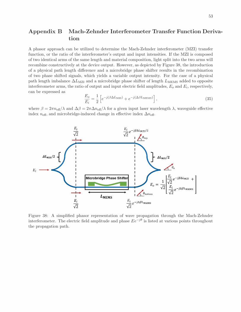
53
Appendix B Mach-Zehnder Interferometer Transfer Function Deriva-tion
A phasor approach can be utilized to determine the Mach-Zehnder interferometer (MZI) transferfunction, or the ratio of the interferometer’s output and input intensities. If the MZI is composedof two identical arms of the same length and material composition, light split into the two arms willrecombine constructively at the device output. However, as depicted by Figure 38, the introductionof a physical path length difference and a microbridge phase shifter results in the recombinationof two phase shifted signals, which yields a variable output intensity. For the case of a physicalpath length imbalance ΔLMZI and a microbridge phase shifter of length LMEMS added to oppositeinterferometer arms, the ratio of output and input electric field amplitudes, Eo and Ei, respectively,can be expressed as
Eo
Ei=1
2
[e−j(βΔLMZI) + e−j(ΔβLMEMS)
], (35)
where β = 2πneff/λ and Δβ = 2πΔneff/λ for a given input laser wavelength λ, waveguide effectiveindex neff, and microbridge-induced change in effective index Δneff.
Figure 38: A simplified phasor representation of wave propagation through the Mach-Zehnderinterferometer. The electric field amplitude and phase Ee−jθ is listed at various points throughoutthe propagation path.

54
Since intensity is proportional to the square of electric field amplitude, the intensity ratio Io/Ii canbe simplified to:
IoIi=1
4
∣∣∣∣e−j(βΔLMZI) + e−j(ΔβLMEMS)
∣∣∣∣2=1
4
∣∣∣∣e−jθtop + e−jθbottom)
∣∣∣∣2=1
4
[2 cos
(θtop − θbottom
2
)]2= cos2
(θtop − θbottom
2
)= cos2
(2πneffΔLMZI
2λ− 2πΔneffLMEMS
2λ
)=1
2
[1 + cos
(2πneffΔLMZI
λ− 2πΔneffLMEMS
λ
)]IoIi=1
2
{1 + cos
[ 2πλ2
(neffΔLMZI −ΔneffLMEMS)︸ ︷︷ ︸kMZI=
2πFSR
λ]}
.
(36)
The period of the resulting sinusoidal spectrum, termed the free spectral range (FSR) is therefore
FSR =λ2
neffΔLMZI −ΔneffLMEMS. (37)
Although the FSR is a function of wavelength, it can be approximated as constant so long as thewavelength range is sufficiently narrow (where “narrow” depends upon the accuracy required).
The group index ng governs the speed of pulse propagation in the MZI and can be written as [13]
ng =λ2
ΔLMZI(FSR). (38)
Substituting the derived FSR, the group index is found to be
ng =neffΔLMZI −ΔneffLMEMS
ΔLMZI= neff − ΔneffLMEMS
ΔLMZI. (39)
Therefore, a decrease in the group index is expected when a microbridge in placed atop one of thewaveguide arms of the interferometer. This shift is experimentally measured in Section 11.

55
Appendix C Theoretical Analysis of the LC Coupled Transducer
C.1 Electromechanical LC Coupled System
To enhance the efficiency of coupling between the input electrical signal and the resulting mechan-ical displacement, the microbridge can also be capacitively coupled to an electronic LC resonator.As a result, the voltage induced across the microbridge from an incident RF signal is magnified,and yields a larger displacement. In this configuration, similar to the bare system, an electricalexcitation displaces the microbridge. As a result, the displacement-dependent parametric capac-itance C(x) of the microbridge changes, yielding a corresponding shift in the electrical resonancefrequency ΩLC = 1/
√LC(x). A schematic diagram of the coupled system is shown in Figure 39.
By tuning the LC resonant frequency to that of the microbridge, the electrical resonator affords asignificant gain enhancement and, when the oscillators are strongly coupled [14], also allows for therealization of physical phenomena such as normal mode splitting and electromechanically inducedtransparency (EMIT) [15, 16].
Figure 39: A schematic diagram of the coupled oscillator system. An electrical excitation potentialVs(t) is injected into the RLC resonator, which displaces the parametric capacitance C(x) formedby the flexible, electrostatically actuated microbridge (blue). The bridge, which is directly biasedby the potential Vdc, is damped at a rate Γm and is displaced by an external noise force Fext(t).
The resulting frequency space transfer function (derived in Appendix A) is
Tcoupled =δΦ(jω)
δVs(jω)=
δX(jω)
δVs(jω)
δΦ(jω)
δX(jω)= −
(2χLC
ΩLCχ0mGemVdc
)(2π
λGomLMEMS
), (40)
where the electromechanical coupling coefficient
Gem =∂ΩLC
∂x
∣∣∣∣x=x0
= − ΩLC
2C(x0)
∂C(x)
∂x
∣∣x=x0
, (41)
in units of rad s−1m−1 describes the strength of coupling between the LC resonance circuit andmechanical microbridge, and
χLC(jω) ≡ δQ(jω)
δVs(jω)
∣∣∣∣δFext=0
=
[1
χ0LC(jω)
− 4V 2dcG
2em
Ω2LC
χ0m(jω)
]−1, (42)
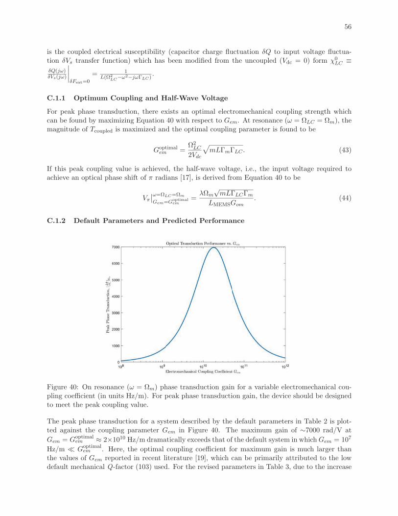
56
is the coupled electrical susceptibility (capacitor charge fluctuation δQ to input voltage fluctua-tion δVs transfer function) which has been modified from the uncoupled (Vdc = 0) form χ0
LC ≡δQ(jω)δVs(jω)
∣∣∣∣δFext=0
= 1L(Ω2
LC−ω2−jωΓLC).
C.1.1 Optimum Coupling and Half-Wave Voltage
For peak phase transduction, there exists an optimal electromechanical coupling strength whichcan be found by maximizing Equation 40 with respect to Gem. At resonance (ω = ΩLC = Ωm), themagnitude of Tcoupled is maximized and the optimal coupling parameter is found to be
Goptimalem =
Ω2LC
2Vdc
√mLΓmΓLC . (43)
If this peak coupling value is achieved, the half-wave voltage, i.e., the input voltage required toachieve an optical phase shift of π radians [17], is derived from Equation 40 to be
Vπ
∣∣ω=ΩLC=Ωm
Gem=Goptimalem
=λΩm
√mLΓLCΓm
LMEMSGom. (44)
C.1.2 Default Parameters and Predicted Performance
Figure 40: On resonance (ω = Ωm) phase transduction gain for a variable electromechanical cou-pling coefficient (in units Hz/m). For peak phase transduction gain, the device should be designedto meet the peak coupling value.
The peak phase transduction for a system described by the default parameters in Table 2 is plot-ted against the coupling parameter Gem in Figure 40. The maximum gain of ∼7000 rad/V at
Gem = Goptimalem ≈ 2×10¹⁰ Hz/m dramatically exceeds that of the default system in whichGem = 107
Hz/m Goptimalem . Here, the optimal coupling coefficient for maximum gain is much larger than
the values of Gem reported in recent literature [19], which can be primarily attributed to the lowdefault mechanical Q-factor (103) used. For the revised parameters in Table 3, due to the increase

57
Parameter Value Description Source
λ 1550 nm Optical wavelength Typical value
[L,w, t]MEMS [75, 250, 3.0] μmLength, width, and thickness of
SiNx MEMS resonator[12]
m ρSiNxLMEMSwMEMStMEMSPhysical mass of MEMS
microbridge[18]
Qm 103MEMS microbridge quality factor
Ωm/Γm[12]
Ωm 2π × 2.3 MHzMicrobridge fundamental resonance
frequency[12]
Vdc 4.3 V DC bridge bias voltage [12]
ΩLC 2π × 2.3 MHzLC resonance frequency (set equal
to Ωm)[12]
R 20Ω RLC circuit resistance [4]
L .64 mH LC inductance [4]
C 1/(LΩ2m)
LC capacitance (set with tuningcapacitor such that ΩLC = Ωm)
[4]
ΓLC R/L LC damping rate Standard value
Gem 107 Hz/mStandard electromechanicalcoupling parameter ∂ΩLC/∂x
[19]
Gom .488 μm−1 Optomechanical couplingparameter ∂neff/∂x
[12]
Table 2: Default parameters for estimating the performance of the coupled RF-to-optical trans-ducer.
Parameter Value Description Source
[L,w, t]MEMS [250, 250, 3.0] μmLength, width, and thicknessof SiNx MEMS resonator
[12]
Qm 104MEMS microbridge quality
factor Ωm/Γm
Reasonable value formicrobridge in vacuum
Ωm 2π × 1.0 MHzMicrobridge fundamentalresonance frequency
Approximate resonantfrequency of 250 micronmicrobridges derived from
FEM simulations
Vdc 5 V DC bridge bias voltageTypical bias voltage before
device pull-in
Gem 108 Hz/mStandard electromechanicalcoupling parameter ∂ΩLC/∂x
Upper bound of FEMsimulation results
Table 3: Revised system parameters based upon the results of the FEM simulations detailed inSection 6. Unlisted parameters are equivalent in value to those listed in Table 2.

58
in Qm to 104, the optimal electromechanical coupling coefficient is on the order of 108 Hz/m – amuch more realistically achievable value.
Assuming that the optimal coupling coupling coefficient is met, the transducer’s half-wave voltageas a function of resonant frequency can be plotted, as in Figure 41 for the parameters in Table 3.The results demonstrate that half-wave voltages on the order of 10 μV should be achievable for1 MHz oscillators, which represents over an order of magnitude improvement compared to recentdevices [4].
Figure 41: Vπ plotted against the resonant frequency Ω = Ωm = ΩLC for the parameters in Table3 assuming the optimal coupling strength is achieved. The results indicate that 10μV half wavevoltages should be achievable for 1 MHz oscillators.
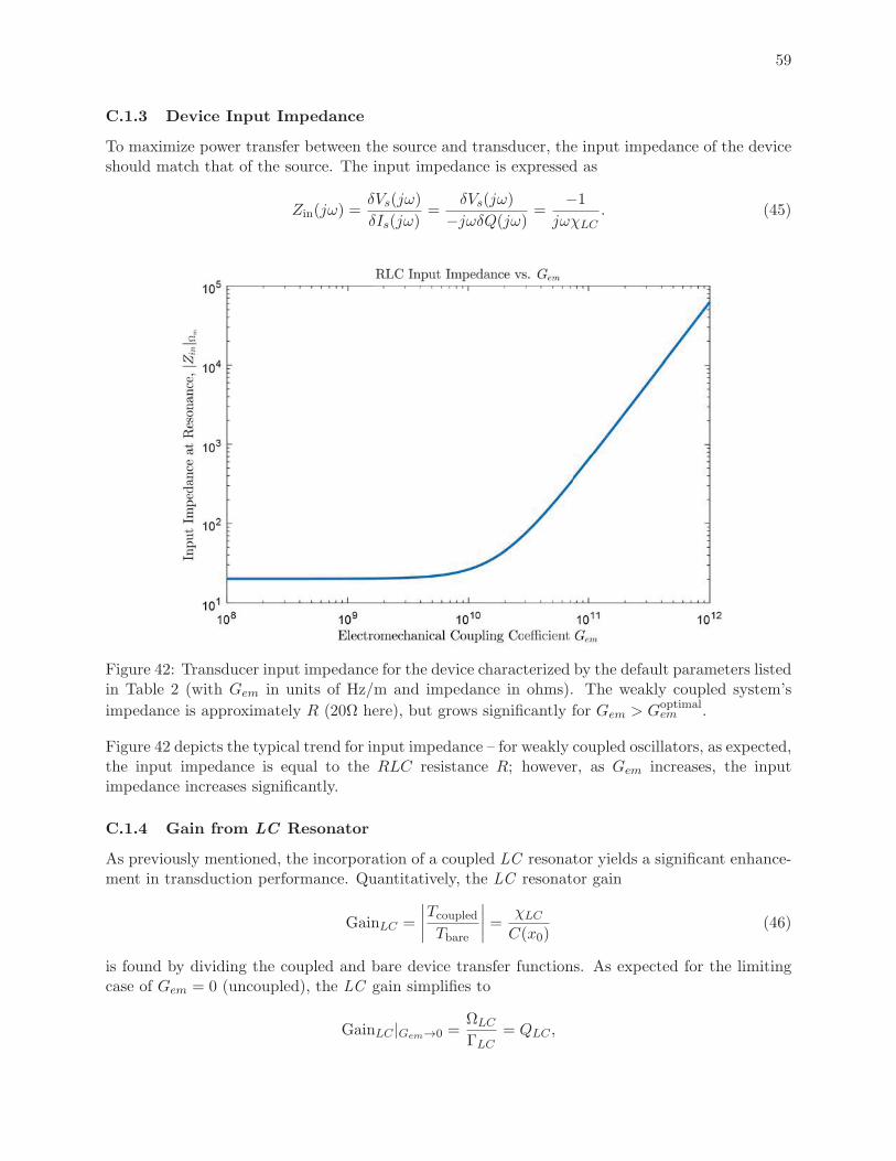
59
C.1.3 Device Input Impedance
To maximize power transfer between the source and transducer, the input impedance of the deviceshould match that of the source. The input impedance is expressed as
Zin(jω) =δVs(jω)
δIs(jω)=
δVs(jω)
−jωδQ(jω) =−1
jωχLC. (45)
Figure 42: Transducer input impedance for the device characterized by the default parameters listedin Table 2 (with Gem in units of Hz/m and impedance in ohms). The weakly coupled system’s
impedance is approximately R (20Ω here), but grows significantly for Gem > Goptimalem .
Figure 42 depicts the typical trend for input impedance – for weakly coupled oscillators, as expected,the input impedance is equal to the RLC resistance R; however, as Gem increases, the inputimpedance increases significantly.
C.1.4 Gain from LC Resonator
As previously mentioned, the incorporation of a coupled LC resonator yields a significant enhance-ment in transduction performance. Quantitatively, the LC resonator gain
GainLC =
∣∣∣∣Tcoupled
Tbare
∣∣∣∣ = χLC
C(x0)(46)
is found by dividing the coupled and bare device transfer functions. As expected for the limitingcase of Gem = 0 (uncoupled), the LC gain simplifies to
GainLC |Gem→0 =ΩLC
ΓLC= QLC ,

60
where QLC is the traditional quality factor of an LC resonator. However, as the electromechanicalcoupling is increased, χLC decreases, and the LC gain rapidly approaches zero. These trends aredepicted for a default system in Figure 43.
Figure 43: LC gain vs. electromechanical coupling coefficient Gem (shown in Hz/m) for the coupled
system described by the default parameters outlined in Table 2 with Goptimalem ≈ 1010 Hz/m. For
Gem Goptimalem , the gain is approximately equal to the quality factor of the LC resonator.

61
Appendix D Transfer Function Behavior, Scaling, and DefaultParameters
Given the coupled device transfer function Tcoupled, the overall transducer gain can be approxi-mated using a set of default parameters derived from recent literature. Table 2 outlines the valueand source of these parameters.
Figure 44: The electrical (left) and optical (right) frequency response for the coupled systemdescribed by the default parameters. On-resonance, the optical response indicates a half wavevoltage of approximately 400 mV.
The electrical and optical response for the transducer characterized by these default parameters areshown in Figure 44. No characteristics of strong coupling, such as EMIT or normal mode splitting,are evident, and the peak phase transduction gain of ∼8 rad/V on resonance yields a half-wavevoltage of approximately 400 mV. However, the system performance can be drastically improvedby increasing the coupling strength and quality of the resonators.
Based on the FEM simulations discussed in Section 6, several default parameters were revised(see Table 3), yielding the modified system response shown in Figure 45. These changes in devicemetrics, most notably an increase in the mechanical quality factor to 104 and a increase of Gem
by an order of magnitude, result in a system with a half-wave voltage of approximately 10 μV.Furthermore, as depicted by the narrow dip on resonance in the electrical frequency response, thestrongly-coupled device illustrates electromechanically induced transparency (EMIT).
D.1 Strong Coupling
As an aside, we briefly summarize the effects which occur when the electrical and mechanicaloscillators are strongly coupled. Strong coupling results in normal mode splitting, i.e. a split in the
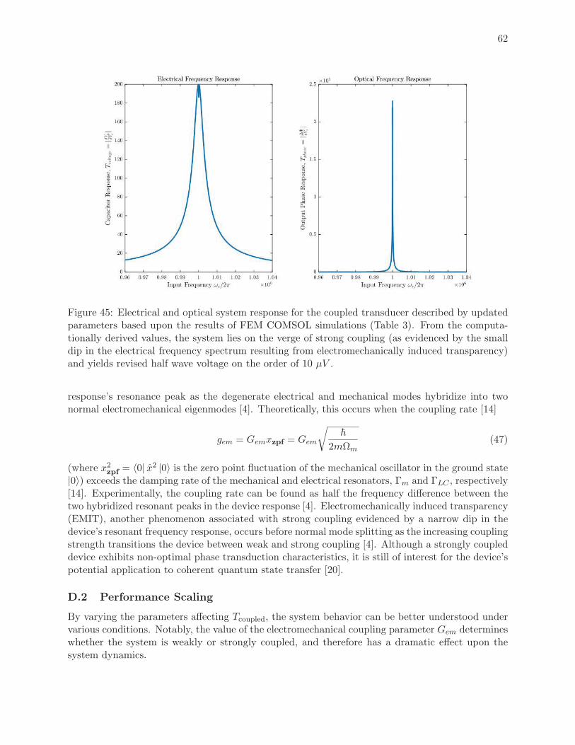
62
Figure 45: Electrical and optical system response for the coupled transducer described by updatedparameters based upon the results of FEM COMSOL simulations (Table 3). From the computa-tionally derived values, the system lies on the verge of strong coupling (as evidenced by the smalldip in the electrical frequency spectrum resulting from electromechanically induced transparency)and yields revised half wave voltage on the order of 10 μV .
response’s resonance peak as the degenerate electrical and mechanical modes hybridize into twonormal electromechanical eigenmodes [4]. Theoretically, this occurs when the coupling rate [14]
gem = Gemxzpf = Gem
√�
2mΩm(47)
(where x2zpf = 〈0| x2 |0〉 is the zero point fluctuation of the mechanical oscillator in the ground state|0〉) exceeds the damping rate of the mechanical and electrical resonators, Γm and ΓLC , respectively[14]. Experimentally, the coupling rate can be found as half the frequency difference between thetwo hybridized resonant peaks in the device response [4]. Electromechanically induced transparency(EMIT), another phenomenon associated with strong coupling evidenced by a narrow dip in thedevice’s resonant frequency response, occurs before normal mode splitting as the increasing couplingstrength transitions the device between weak and strong coupling [4]. Although a strongly coupleddevice exhibits non-optimal phase transduction characteristics, it is still of interest for the device’spotential application to coherent quantum state transfer [20].
D.2 Performance Scaling
By varying the parameters affecting Tcoupled, the system behavior can be better understood undervarious conditions. Notably, the value of the electromechanical coupling parameter Gem determineswhether the system is weakly or strongly coupled, and therefore has a dramatic effect upon thesystem dynamics.

63
Figure 46: System response for varying coupling strengths. Peak phase transduction is achieved atthe optimal coupling strength (Gem ≈ 1010 Hz/m. Past the optimum coupling rate, the oscillatorsbecome strongly coupled, as evidenced by the normal mode splitting seen within the electrical andoptical responses.
Figure 47: The system response resulting from an increased mechanical quality factor Qm = 105.In this case, an optimal coupling coefficient value is clearly evident, since phase transduction issignificantly damped for the instances of normal mode splitting.

64
Figure 46 demonstrates the change in the device’s frequency response when Gem is swept acrossseveral orders of magnitude. Initially, when Gem 1010 Hz/m, increasing the coupling strengthyields a direct improvement in the peak phase transduction as shown in the RHS of Figure 46. How-ever, further increases in Gem past the peak value discussed in Section C.1.1 (∼ 1010 Hz/m here)yield a normal mode splitting as depicted by the two resonant peaks in Figure 46 for Gem = 1011
Hz/m.
The presence of an optimum coupling strength becomes readily apparent when considering higher-Q oscillators. Figure 47 demonstrates this effect for a modified system with Qm = 105. Here, theonset of EMIT for Gem = 1010 Hz/m is clearly visible, yielding a peak phase gain of nearly oneorder of magnitude larger than the strongly coupled system for higher values of Gem. Therefore,these results not only depict two phenomena associated with strongly coupled oscillators, but alsofurther manifest the necessity of achieving the optimal coupling strength discussed in Section C.1.1in order to realize peak transduction gain.

65
Appendix E Simulated Performance of LC -based System
E.1 Electromechanical Coupling
From the results of the DC bias study, the electromechanical coupling parameterGem = − ΩLC2C(x)
∂C(x)∂x
∣∣x=x0
can be readily calculated. The results for each bridge length and bias point are shown in Figure48. As expected, the coupling strength increases as the bridge is displaced further downwards(i.e., as Vdc increases). Although ∂C(x0)/∂x increases for longer bridges, the decrease in resonantfrequency outweighs this improvement, and the coupling strength thus favors shorter bridge lengths.
Figure 48: Electromechanical coupling parameter Gem for the bridge lengths studied in the DCbias analysis. As the bias approaches the pull-in voltage, the electromechanical coupling strengthgrows, as Gem ∝ ∂C(x)
∂x . It should be noted that a constant resonant frequency is assumed for eachbridge length (i.e. not accounting for capacitive spring softening).
These coupling strengths can be compared to the optimal values derived in Section C.1.1. Figure49 demonstrates that for both the original parameters listed in Table 2 as well as for improvedresonator Q-factors listed in Table 3, the resulting electromechanical coupling strengths both fallshort of the optimal values desired.
Based on the theoretical results provided in Appendix C, the parameters affecting optimal systemdesign can be investigated. For a system specifically intended to minimize the half-wave voltage,Equations 41, 43, and 44 define the design parameters of greatest importance. In order to minimizethe required optimal coupling strength for peak performance (maximum phase transduction gain),the system resonant frequency should be minimized. Furthermore, the mass of the microbridge,damping rates of the respective oscillators, and LC inductance should all be minimized. In con-trast, to attain the optimal coupling condition, we seek to maximize Gem. The electromechanicalcoupling coefficient can be increased by: 1) increasing the resonant frequency (in opposition to
the minimization sought for Goptimalem ); 2) minimizing the total capacitance; or 3) designing the
capacitor geometry and appropriately biasing the device to maximize ∂C(x)/∂x. A brief overview
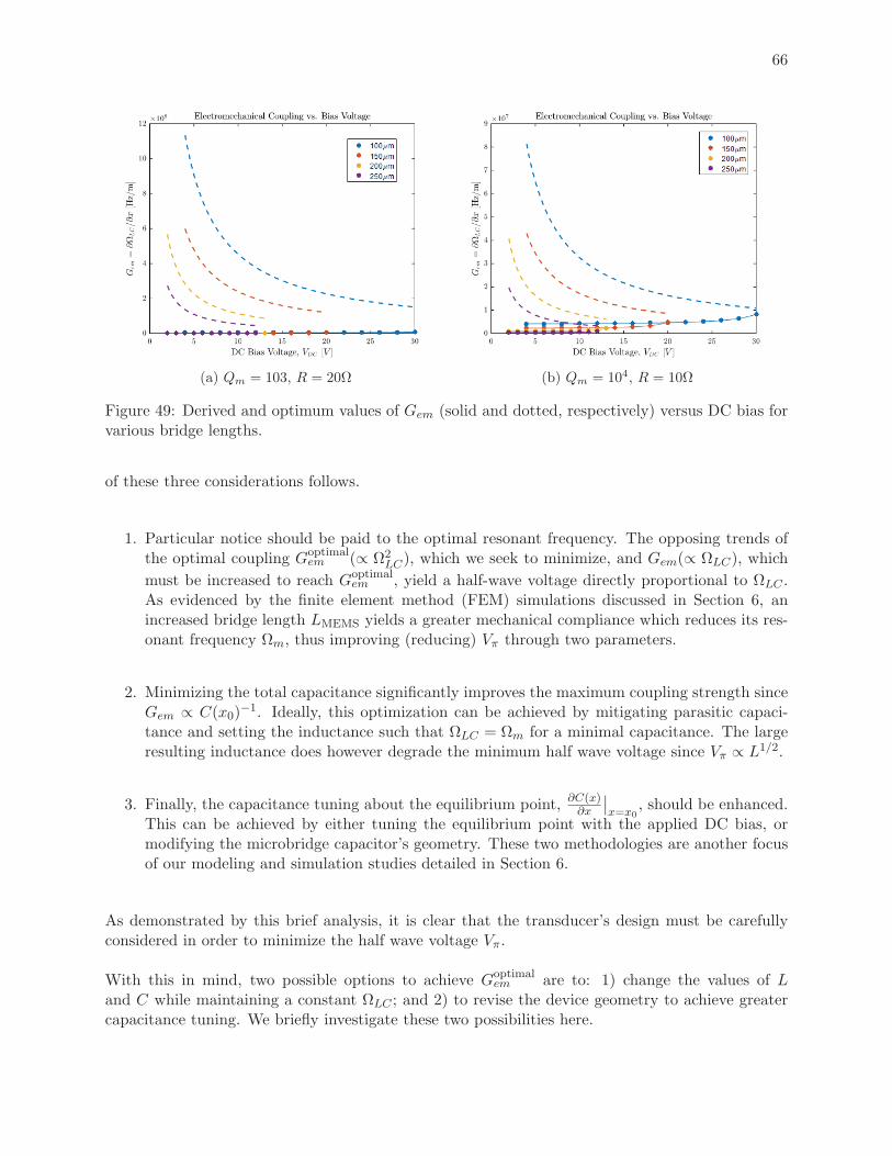
66
(a) Qm = 103, R = 20Ω (b) Qm = 104, R = 10Ω
Figure 49: Derived and optimum values of Gem (solid and dotted, respectively) versus DC bias forvarious bridge lengths.
of these three considerations follows.
1. Particular notice should be paid to the optimal resonant frequency. The opposing trends ofthe optimal coupling Goptimal
em (∝ Ω2LC), which we seek to minimize, and Gem(∝ ΩLC), which
must be increased to reach Goptimalem , yield a half-wave voltage directly proportional to ΩLC .
As evidenced by the finite element method (FEM) simulations discussed in Section 6, anincreased bridge length LMEMS yields a greater mechanical compliance which reduces its res-onant frequency Ωm, thus improving (reducing) Vπ through two parameters.
2. Minimizing the total capacitance significantly improves the maximum coupling strength sinceGem ∝ C(x0)
−1. Ideally, this optimization can be achieved by mitigating parasitic capaci-tance and setting the inductance such that ΩLC = Ωm for a minimal capacitance. The largeresulting inductance does however degrade the minimum half wave voltage since Vπ ∝ L1/2.
3. Finally, the capacitance tuning about the equilibrium point, ∂C(x)∂x
∣∣x=x0
, should be enhanced.This can be achieved by either tuning the equilibrium point with the applied DC bias, ormodifying the microbridge capacitor’s geometry. These two methodologies are another focusof our modeling and simulation studies detailed in Section 6.
As demonstrated by this brief analysis, it is clear that the transducer’s design must be carefullyconsidered in order to minimize the half wave voltage Vπ.
With this in mind, two possible options to achieve Goptimalem are to: 1) change the values of L
and C while maintaining a constant ΩLC ; and 2) to revise the device geometry to achieve greatercapacitance tuning. We briefly investigate these two possibilities here.

67
E.2 Achieving Optimal Electromechanical Transduction – Varying L
Figure 50: As depicted by the intersection of the optimal and simulated coupling curves (shown asblack points), changing the LC circuit inductance from .64 mH to 5 mH enables optimal couplingto be achieved.
Assuming an LC inductance on the order of 1 mH (coinciding with the value listed in [4]), therequired capacitance for a 1 MHz oscillator is on the order of 10 pF. Since the microbridge ca-pacitance is roughly on the order of fF, a parallel tuning capacitor, which accounts for the vastmajority of the circuit’s overall capacitance, is required to achieve the desired resonance frequency[4]. By increasing the inductance, the required capacitance of this tuning capacitor, and thereforethe overall capacitance, decrease significantly. Since Gem ∝ C(x0)
−1, this decrease in capacitanceaccounts for an increase in the coupling strength. The coupling strength resulting from incorpora-tion of a larger 5 mH inductor (compared to the default value of .63 mH) is depicted in Figure 50.As indicated by the intersection of the simulated and optimal coupling curves, the experimentalsystem should be able to be biased at the optimal coupling point for all simulated bridge lengths.As the bias voltage increases beyond optimal coupling, the results similarly indicate the possibilityof achieving strong coupling.
Thus, these results clearly illustrate that a tunable inductance yields a feasible mechanism bywhich the coupling strength can be modified, and by which the transducer bias point can be variedbetween weak, optimal, and strong coupling regimes.
E.3 Achieving Optimal Electromechanical Transduction – Revised Geometry
Alternatively, the coupling strength can also be improved by optimizing the geometry. To increasethe change in capacitance for a given displacement, the direct electrostatic geometry was modifiedby decreasing the height of the microbridge from 230 nm to 100 nm and decreasing the horizontalstandoff distance of the side electrode from 1 micron to 100 nm. The principal advantage of the

68
Figure 51: Gem vs. Vdc comparison between the original and modified electrostatic geometries.The optimal coupling parameter value, plotted in orange given the revised parameters in Table 3,is only met by the modified geometry.
optimized geometry is an improvement in capacitance tuning. Figure 51 illustrates that this en-hancement enables the realization of optimal electromechanical coupling. Based upon the limits offabrication, the geometry could be further modified to improve the coupling strength.
E.4 Summary
In this section, we compared the simulation-derived electromechanical coupling coefficient Gem toits optimal value set by Equation 43. Since the simulated coupling coefficient does not obtain theoptimal value for either the bare or enhanced parameters established in Tables 2 and 3, respectively,two alternative optimization methods are investigated: 1) readjusting the ratio of capacitance toinductance in the LC circuit and 2) revising the microbridge geometry. Both of these methods areshown to improve Gem enough to achieve the optimal coupling value, thus maximizing transductiongain and minimizing the resulting Vπ.

69
Appendix F Comparison of Electrostatic Actuation Techniques
As opposed to direct electrostatic actuation using a bridge and side electrode, the Kelvin polarization-force based geometry can be utilized to electrostatically actuate the microbridge [22]. By conductinga DC bias study of this geometry with a 100 micron bridge, the scheme’s efficiency can be com-pared to that of direct electrostatic actuation. The results, shown in Figure 52, indicate that thedefault gradient electric field actuation geometry is a less apt technique for sensitive transductionapplications. Not only are the DC bias and required energy an order of magnitude greater thanthose of the direct actuation geometry, but the capacitance tuning is also significantly degraded.
The actuation efficiency can, however, be improved by moving the bias electrodes closer together.Figure 53 depicts the improved performance that results as the separation decreases from the defaultvalue of 4 microns – the pull-in bias is significantly reduced, and the capacitance tuning increasessignificantly. An exception to this general trend of improvement exists between the displacementsof 4 and 5 microns, which could be an artifact of the FEM simulation conducted. Despite theimprovement, the coupling strength of the direct actuation scheme still dominates the polarization-based technique.
The predominant advantage of a Kelvin polarization force-based geometry is the noninvasive ac-tuation – no electrode, and therefore bias probe, needs to be mounted onto the bridge [30]. Thebridge’s Q-factor is therefore preserved, and the actuation technique can be used on an array of ar-bitrary MEMS geometries [4, 22]. For our application, the degradation of the mechanical resonatorresulting from the application of an electrode and bias probe should be carefully analyzed in orderto determine it’s significance – if it induces a substantial performance decay, the polarization-basedactuation scheme may yield a more feasible technique.
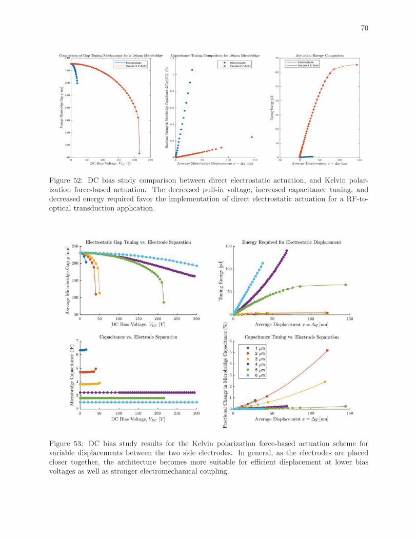
70
Figure 52: DC bias study comparison between direct electrostatic actuation, and Kelvin polar-ization force-based actuation. The decreased pull-in voltage, increased capacitance tuning, anddecreased energy required favor the implementation of direct electrostatic actuation for a RF-to-optical transduction application.
Figure 53: DC bias study results for the Kelvin polarization force-based actuation scheme forvariable displacements between the two side electrodes. In general, as the electrodes are placedcloser together, the architecture becomes more suitable for efficient displacement at lower biasvoltages as well as stronger electromechanical coupling.

71
Appendix G Microbridge Design Optimization
The doubly-clamped microbridge used for these investigations suffers from several drawbacks. Thetwo suspension points, for example, prevent the bridge from having a uniform deflection profilealong its length, which results in a undesired variation in the optical effective index across thelength of the optomechanical interaction region. Furthermore, the doubly-clamped architectureyields a non-optimal pull in voltage and requires specially designed supports to avoid interferencewith the waveguide placed below the suspended bridge. To address these limitations, an alterna-tive cantilever-supported design was investigated. For this architecture, five 30 micron long, 0.75micron wide, and 150 nm thick cantilevers – fixed at one end to a side support and connected tothe suspended microbridge at the other – we placed at uniform intervals on each side along thelength of the bridge.
Due to the reduced spring constant of the cantilevers compared to the spring constant of theoriginal doubly-clamped bridge, an applied bias results in a greater deflection across the length ofthe cantilevers than across the microbridge, yielding a more uniform displacement across the lengthof the microbridge. Figure 54, which compares the two designs, demonstrates that the central(center 10%, or 10 microns for a 100 micron-long bridge) displacement is reduced to under 20%of its original value when the cantilever design is implemented. Additionally, the pull-in voltageis reduced by an order of magnitude, indicating that, for a constant applied voltage, a greaterdisplacement is induced in the optimized structure than in the original. The overall transductiongain, which is a function of the electrostatic coupling efficiency, is therefore improved. Overall, thisexperiment demonstrates that a judicious choice of perturber design parameters can significantlyimprove transduction efficiency.

72
(a) Original doubly-clamped beam.
(b) Optimized cantilever-suspended beam.
Figure 54: FEM simulated displacement profiles for an electrostatically actuated 100 micron doubly-clamped beam suspended 230 nm above the substrate (a). Within the central 10 microns, the heightvaries by less than 3 nm. To achieve a flatter bridge profile, a cantilever-suspended beam design wascreated with ten 30 micron-long cantilevers (b), yielding nearly an order of magnitude reduction inboth actuation voltage and height variation with the central region.

73
Appendix H Optomechanical Coupling Optimization
The optomechanical coupling parameter Gom ≡ ∂neff∂x dictates the effectiveness of the microbridge
effective index tuning mechanism. Since the half wave voltage of the mechanically mediated trans-ducer is inversely proportional to Gom, we explore the optimization of this coupling parameter byanalyzing 1) the waveguide dimensions, 2) the perturber characteristics, and 3) the addition of afield-enhancing high-index film to the waveguide.
H.1 Waveguide Optimization
By varying the dimensions of the silicon nitride waveguide, we can determine the waveguide size thatminimizes the optical confinement, defined by the ratio of the optical energy density W integratedover the waveguide to that integrated over the entire mode area [13]
Γ =
∫∫WG |W |dA∫∫mode |W |dA
. (48)
When this ratio is minimized, the percent of optical power in air is maximized, leading to optimumindex tuning efficiency since the microbridge interacts with a larger evanescent field.
Figure 55: The optomechanical coupling factor Gom as a function of the waveguide core thicknessand the microbridge-waveguide gap. A constant 31% etch depth is assumed. Note that the couplingis maximized for a waveguide core thickness of approximately 175 nm. The maximum value is onthe order of 106 m−1.
Parametric sweeps of the rib waveguide core thickness, etch depth (as a percentage of the corethickness), and core width were conducted. While the etch depth and core width had little effecton the tuning performance, varying the waveguide core thickness yielded a significant change in

74
the optical confinement. The results, shown in Figure 55, confirm the previous determination [11]of an optimal core thickness tCore ≈ 170 nm.
H.2 Perturber Optimization
Similarly, the dimensions of the microbridge perturber can also be varied to determine their ef-fect on Gom. Increasing the microbridge thickness tMEMS, for example, lends to a correspondingimprovement in optomechanical coupling as shown in Figure 56. However, the thickness of theperturber cannot be increased without bound since beyond a critical thickness the microbridgebecomes an independent waveguide and can itself support a propagating optical mode, yieldingsignificant optical loss [12].
Figure 56: As the perturber’s thickness increases, the optomechanical coupling increases, as moreoptical power from the waveguide’s evanescent field is confined within the microbridge.
H.3 Thin Film High-Index Cladding
The percent of optical power in air, and thus the efficiency of the microbridge coupling to theevanescent field, can also be optimized by coating the waveguide with a thin high-index film. Thistechnique has been successfully implemented in previous evanescent field sensing devices, and hasbeen found to increase the peak intensity of the electric field at the waveguide-air interface by anorder of magnitude [45, 46].
The results of our mode simulations, shown in Figure 57, confirm this experimental conclusion.Figures 58 and 59 depict the resulting enhancement in the optomechanical coupling factor when athin film coat (n = 4.0) of variable thickness is applied to the waveguide. A peak improvement in
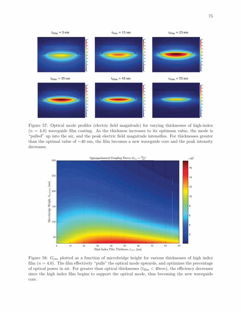
75
Figure 57: Optical mode profiles (electric field magnitude) for varying thicknesses of high-index(n = 4.0) waveguide film coating. As the thickness increases to its optimum value, the mode is“pulled” up into the air, and the peak electric field magnitude intensifies. For thicknesses greaterthan the optimal value of ∼40 nm, the film becomes a new waveguide core and the peak intensitydecreases.
Figure 58: Gom plotted as a function of microbridge height for various thicknesses of high indexfilm (n = 4.0). The film effectively “pulls” the optical mode upwards, and optimizes the percentageof optical power in air. For greater than optical thicknesses (tfilm < 40nm), the efficiency decreasessince the high index film begins to support the optical mode, thus becoming the new waveguidecore.

76
Figure 59: For the optimal thickness of approximately 40 nm, the peak value of the optical couplingcoefficient increases by over 60% through the application of a high index (n = 4.0) waveguidecoating film. However, for waveguide-perturber gaps greater than ∼200 nm, the application of thehigh-index film actually reduces transduction sensitivity.
Gom of over 60% for a 40 nm thick film was found, thus confirming the validity of the technique tomaximize the optomechanical coupling performance.

77
Appendix I Experimental Challenges – Stiction Failure
Prior to experimental testing, the development of theoretical device transfer functions enabled theexploration of optimum RF-to-optical transduction performance for two different systems, one withan LC resonator and one without. Furthermore, computational simulations verified the feasibilityof achieving the optimal bias point required for peak transduction gain. Having completed theseanalysis, we now explore the experimental characterization of fabricated devices.
Originally, an existing fabricated electro-optomechanical chip used in previous studies, was to bere-purposed for these experiments. Prior to electrically actuating the devices or conducting anyoptical testing, an optical profilometer was used to characterize the structural integrity of the pre-viously used devices. Profilometry scans of each bridge revealed that all of the previously usablemicrobridges had been pulled into contact with the underlying waveguides, and were bonded tothem by internal forces. This failure mechanism, commonly known as “stiction,” has been cited asa common mode of failure for MEMS devices [38, 39]. Sample results from the optical profilometrytesting are shown in Figure 60, which contrasts the flat bridge elevation profile of a suspendedbridge to the bowed profile of a stiction-failed bridge.
(a) Suspended Bridge (b) Stiction Failed Bridge
Figure 60: Optical profilometry scans of 40 micron long microbridge which was initially suspended(a) and subsequently experienced stiction-induced failure (b), which can be noted by the depressedbridge elevation throughout the length of the bridge.
To conduct any further testing, suspended bridges were required. Several attempts to repair thestiction-failed bridges were thus conducted using a variety of techniques. Initial trials consisted ofapplying a downward-sloping linear frequency modulated chirp RF signal to the bridge, an ideaproposed in [40]. In this fashion, the initially high frequency of the signal would match the reso-nant frequency of the “unstuck” portion of the bridge, thus effectively vibrating it and potentiallydecreasing the length of the stuck portion of the bridge. The decreasing frequency would thencontinue to match the resonant frequency of the lengthening suspended beam until the bridge wascompletely unstuck. However, this technique prove ineffective for the failed devices, as the bridgeswere almost completely adhered to the underlying waveguide. Another alternative repair technique

78
attempted was heating the devices with a hot plate. The thermal expansion expected from heatingwould further tension the bridge, and possibly provide the restoring force required to unstick thebridge. Despite heating to 110◦C, this technique failed to free any bridges. Other published repairtechniques, such as laser-induced stress wave recovery [41, 42], were not pursued due to lack ofrequired equipment. Finally, the sample chip was immersed in a isopropyl alcohol and placed inan ultrasonic bath in an attempt to vibrate the MEMS microbridges free. After a one hour soni-cation, the sample was dried with a critical point dryer, and the bridge profiles were subsequentlyreevaluated with the Zygo optical profilometer.
Although this final technique led to the repair of one device, fabrication of a new sample waspursued as an alternative course of action.

79
Appendix J Experimental Challenges – Electrical Pickup Isola-tion
When the bias probes were connected to the initial microbridge devices as shown in Figure 28, alarge amplitude, low frequency oscillation was noted in the the optical output even when no biasvoltage – DC or RF – was applied. By taking a discrete Fourier transform of the photodetectoroutput sampled by the benchtop digital multimeter, we were able to determine that the pickupconsisted primarily of 60 Hz noise and its associated higher frequency harmonics (blue spectrum inFigure 61a).
(a) Device 12 (75 micron bridge; probes connected) noise spectrum with and without optical table grounded.
(b) Device 9 (50 micron bridge) noise spectrum with and without probes connected.
Figure 61: (a) When bias probes were connected the device, 60 Hz electrical pickup was modulatedonto the optical output. This signal was significantly attenuated when the electrically-floatingoptical table was grounded to the benchtop DC bias source (red curve). (b) Further isolationprovided by aluminum foil shielding placed around open electrical components yielded minimalnoise variation between the output with and without probes connected.

80
In the process of measuring the floating potential of various objects throughout the room, the opti-cal table was found to be electrically-floating with an RMS voltage of nearly 0.4V. After connectingthe metal table to the ground port of the DC bias source, thereby tying the entire lab apparatusto the building’s AC ground, the optical response to the pickup was attenuated by nearly 30 dB(red curve in Figure 61a).
Aluminum foil was then wrapped around the exposed ground connections of the electrical biasinstruments and components to further reduce the electrical pickup. The final result, depicted inFigure 61b, was a nearly identical noise level in the optical output when the electrical probes wereeither connected or disconnected. While this noise issue emerged as a experimental challenge, it alsodemonstrated the viability of the intended device functionality – optical detection of low-frequencyelectrical signals.